Article

Formation of Aligned α-Si3N4 Microfibers by Plasma Nitridation of Si (110) Substrate Coated with SiO2

1
Department of Materials Science and Engineering, National Yang Ming Chiao Tung University, Hsinchu 30010, Taiwan
2
National Applied Research Laboratories, Taiwan Instrument Research Institute, Hsinchu 30010, Taiwan
*
Authors to whom correspondence should be addressed.
Coatings 2021, 11(10), 1251; https://doi.org/10.3390/coatings11101251
Submission received: 18 August 2021 / Revised: 6 October 2021 / Accepted: 7 October 2021 / Published: 14 October 2021
(This article belongs to the Section Ceramic Coatings and Engineering Technology)

Abstract

:
Plasma nitridation of an amorphous SiO2 layer on Si (110) substrate can form well-aligned α-Si3N4 crystallites in fibrous morphology. Nitriding is performed at a temperature in the range of 800–1000 °C by using microwave plasma with a gas mixture of N2 and H2. Raman spectroscopy shows the characteristics of an α-Si3N4 phase without other crystalline nitrides. As shown by scanning electron microscopy, the formed α-Si3N4 microfibers on the Si substrate can be in a dense and straight array nearly along with Si < 1 1 ¯ 0 >, and can have a length over 2 mm with a diameter in the range of 5–10 μm. Structural characterization of scanning transmission electron microscopy in cross section view reveals that the elongated α-Si3N4 crystallites are formed on the surface of the nitrided SiO2/Si (110) substrate without any interlayers between Si3N4 and Si, and the longitudinal direction of α-Si3N4 appears mainly along < 11 2 ¯ 0 >, which is approximately parallel to Si < 1 1 ¯ 0 >.

1. Introduction

Silicon nitride (Si3N4) has been used in many structural applications for a long time due to its excellent properties, such as high hardness and high-temperature stability, resistance to thermal shock, and wear resistance. In addition, Si3N4 has a wide band gap (Eg = 4.7 eV) which can be applied for semiconductor devices [1,2]. Si3N4 has many different crystal structures, among which α-Si3N4, β-Si3N4, and γ-Si3N4 are common phases. Both α-Si3N4 and β-Si3N4 can be formed under ambient conditions at high temperatures, while γ-Si3N4 exists under high temperature and high pressure [3,4,5]. In addition, crystalline Si3N4 synthesis, generally in polycrystalline microstructure, has been widely conducted by nitridation of Si and SiO2 powders at high temperature. Plasma nitriding has been proven to be effective for material synthesis [6,7,8]. Plasma nitridation of SiO2 and Si for the formation of Si3N4 have been studied in previous reports by using thermal and radio frequency plasma processes with gases containing nitrogen [9,10,11] in which hydrogen may be necessary for the oxide reduction, and nitrogen reaction with Si formed nitride. It is well known that microwave plasma can easily achieve high plasma density which has been applied in various applications, including etching and film deposition. In our recent studies, we have shown that microwave plasma can be effectively applied for nitridation of c-plane and m-sapphires to form epitaxial AlN. In addition, epitaxial TiN can obtain plasma nitridation of rutile TiO2 [12,13,14].
Various forms of crystalline Si3N4 have been synthesized, including whiskers and nanowires which may have potential applications in nanocomposites and electronic devices. Si3N4 nanowires have been synthesized by various methods, including chemical vapor deposition and nitridation [15,16,17,18]. Recently, we have used microwave plasma for nitridation of a SiO2/Si (111) substrate to form { 10 1 ¯ 0 }-oriented crystalline α-Si3N4 and β-Si3N4 which have elongated wire morphologies in lengths of several hundred micrometers and are mainly aligned with three different Si <110> directions [19]. In this study, the formation of crystalline Si3N4 on an Si (110) substrate which was coated with SiO2 was investigated. Furthermore, we try to understand the role of Si orientation on the alignment of Si3N4. The results showed that crystalline α-Si3N4 microfibers in aligned arrays with a length more than 2 mm are mainly formed along a unique direction of Si < 1 1 ¯ 0 > on Si (110).

2. Materials and Methods
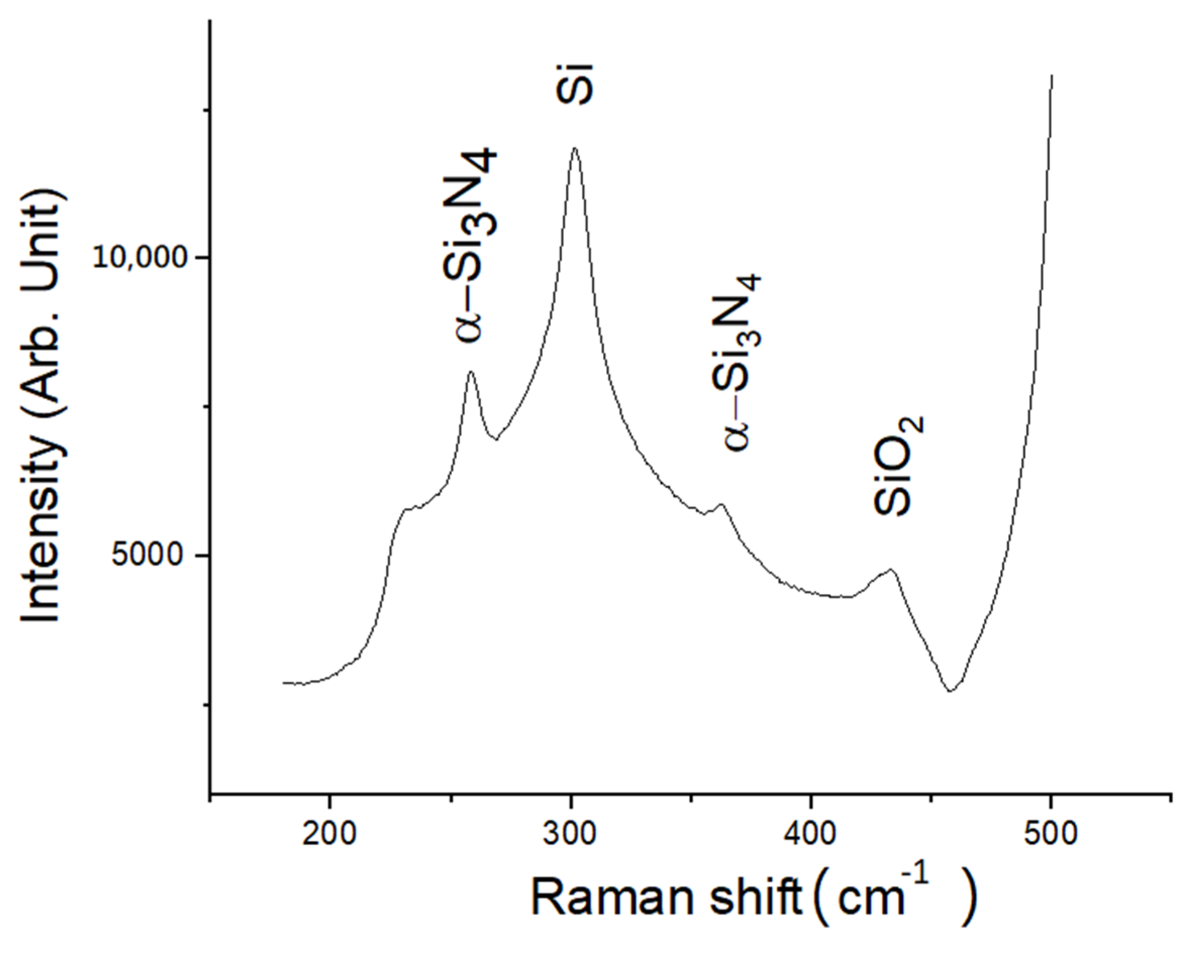
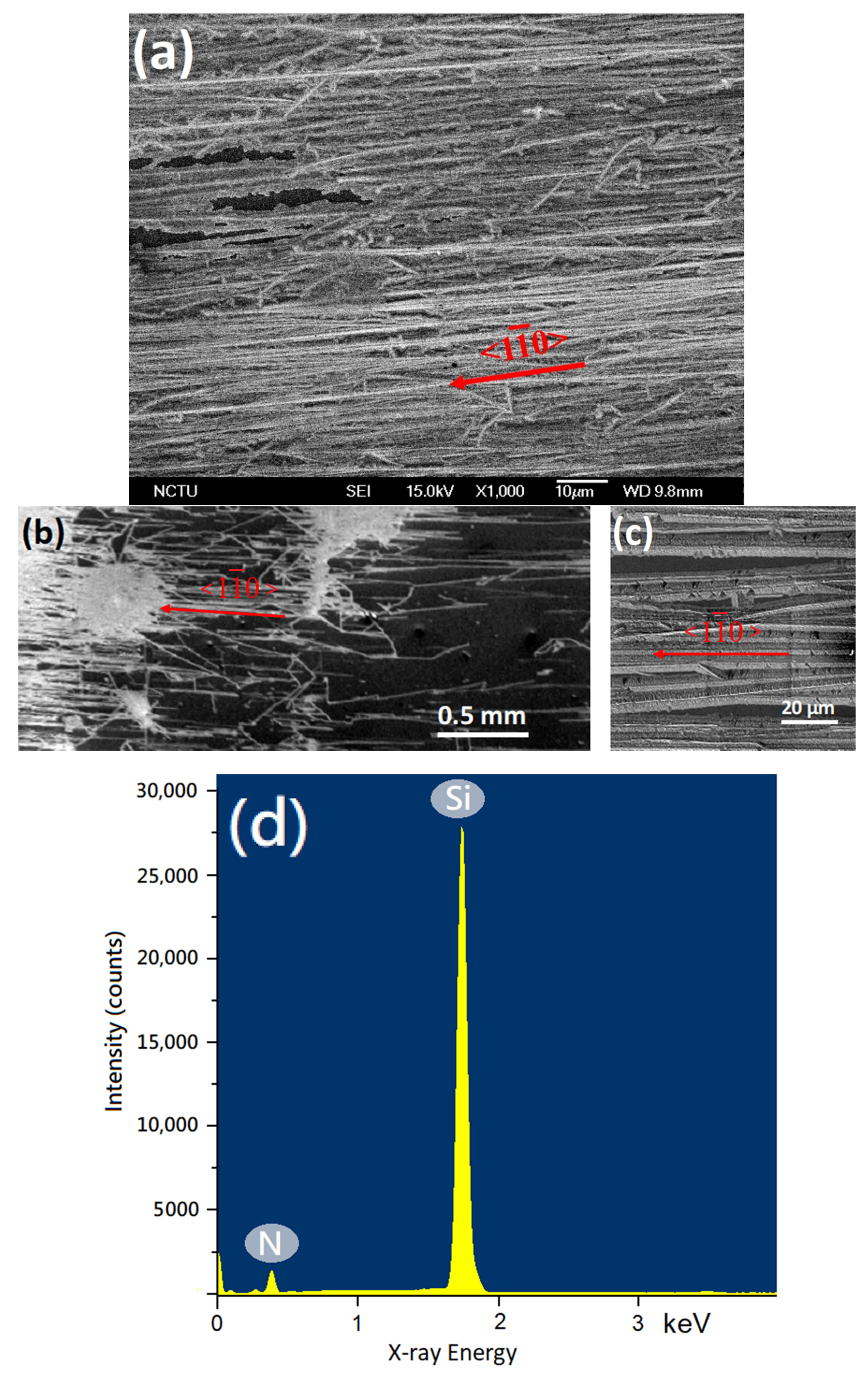
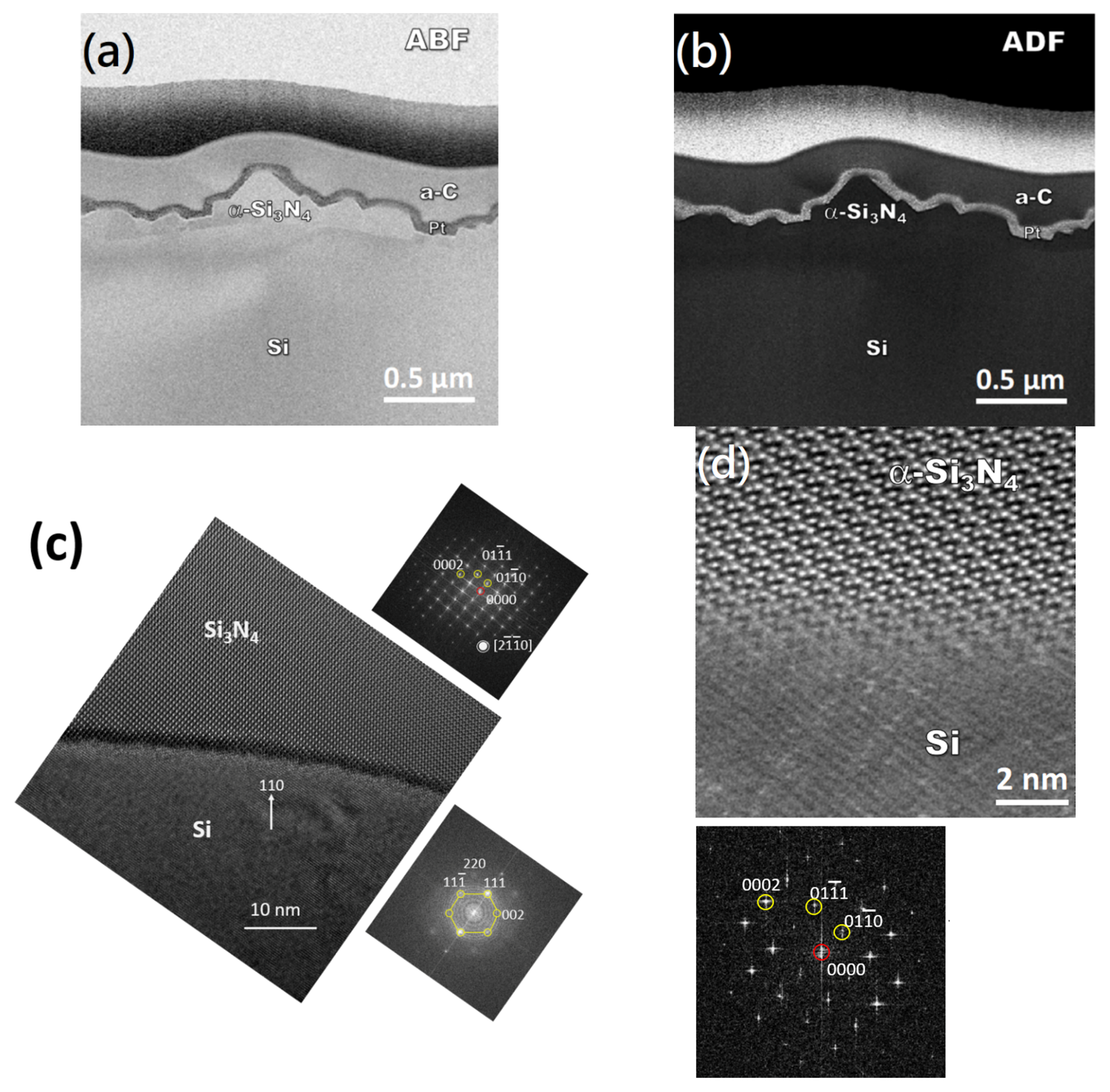
In this work, a 50 nm thick SiO2 film grown on a two inch Si (110) wafer was used as substrate. Growth of the SiO2 film was performed at 300 °C by plasma-enhanced chemical vapor deposition using a gas mixture of SiH4, N2O, and Ar. After the deposition of SiO2, the substrate was cut to pieces about 1 × 1 cm2. Nitridation of the SiO2/Si (110) substrate with a gas mixture of N2 and H2 was performed in a microwave (2.45 GHz) plasma system, which was commonly employed for chemical vapor deposition of diamond [20,21]. The flow rate of N2 and H2 was 285 and 15 sccm, respectively. The microwave power was set at 700 W and a pressure of 5.3 × 10³ Pa. The nitridation was carried out for 10 and 20 min. The substrate temperature during plasma nitriding was estimated to be in the range of 800–1000 °C as measured by optical pyrometer (wavelength of 0.96 µm).
Raman spectroscopy was carried out in a Horiba Jobin Yvon LabRAM HR 800 spectrometer with 50 mW Ar laser (λ = 533 nm). Scanning electron microscopy (SEM, JEOL JSM-6500F, Tokyo, Japan). was performed to examine surface morphologies of the SiO2/Si (110) substrates. Cross-sectional scanning transmission electron microscopy (ARM200F, JEOL, Tokyo, Japan) with high-resolution transmission electron microscopy (HRTEM) was performed for crystallographic evaluation. Cross-sectional STEM specimen preparation was performed in a dual-beam focused ion beam (FIB, TESCAN LYRA3) system. Before FIB cutting, a 50 nm thin layer of amorphous carbon (a-C) and a 240 nm layer of platinum (Pt) were deposited on the nitride sample surface with an electron beam, followed by deposition of a 250 nm layer of a-C and a 300 nm layer of Pt with ion beam as protective coating.

3. Results

Figure 1a shows a typical SEM micrograph of the nitrided SiO2/Si (110) substrate after 10 min nitriding. The surface morphology shows that Si3N4 crystallites exhibit a fiber-like characteristic with an average diameter of about 1–2 μm and a length of >0.1 mm. Those Si3N4 microfibers are predominately aligned in parallel with each other and approximately along the specific direction of Si [ 1 1 ¯ 0 ]. For 20 min nitridation, the length of the microfibers can be as long as 2 mm and the diameter can increase to 5–10 μm, as shown in Figure 1b,c. A few areas on the nitrided substrate are covered with highly dense microfibers. The microfibers shown in Figure 1c exhibit a prism-like morphology, and most of the microfibers are aligned nearly with their longitudinal directions Si [ 1 1 ¯ 0 ] in addition to a few deviated ones. The faceted morphology suggests that the microfibers are of the crystalline phase. Furthermore, X-ray energy dispersive spectroscopy shows that those microfibers consist of Si and N, as shown in Figure 1d, with the absence of O, implying that SiO2 may not exist anymore after nitriding.
Raman spectra from different areas on the SEM images shown in Figure 1 were acquired in micromode. A typical Raman spectrum acquired from the microfibers is shown in Figure 2 from 150 to 450 cm−1. The Raman peaks observed at 259 and 363 cm−1 are identified to belong to α-Si3N4 [22]. The Raman peak at 300 cm−1 is the characteristic signal of Si in second order [23,24]. As no β-Si3N4 characteristic peaks are observed, it is evident that all the microfibers are of the α-Si3N4 phase. On the bare area without coverage of the Si3N4 crystallites as shown in Figure 1b, neither Si3N4 nor SiO2 Raman signals can be observed, implying that SiO2 after nitridation might transform to Si3N4, or be etched away by the plasma containing hydrogen. Many of the glass vibrations are known to occur between 400–700 cm−1 (bridging Si-O-Si vibrations) which are not seen in the spectrum [24].
Figure 3 shows typical cross-sectional TEM/STEM images from the nitrided sample for 20 min nitridation after tilting about 7° away from the Si [ 1 1 ¯ 0 ] zone axis with the edge-on orientation for the Si3N4/Si interface. Figure 3a,b show low-magnification annular bright field (ABF) and annular dark field (ADF) images in diffraction and atomic number contrast, respectively. As can be seen, the Si3N4 thickness is varied from 70 to 270 nm, and no interlayers exist between Si3N4 and Si. Figure 3c shows a typical high-resolution TEM (HRTEM) image taken from the central region in Figure 3a where the thickness is about 270 nm after tilting about 2° away from the Si [ 1 1 ¯ 0 ] zone axis to align Si3N4 in [ 2 1 ¯ 1 ¯ 0 ] the zone axis. The HRTEM image shows that Si3N4 is in direct contact with Si though the interface between them is not flat. The corresponding fast Fourier transform (FFT) pattern from Si3N4 shown in the upper inset demonstrates that Si3N4 is an α-phase in [ 2 1 ¯ 1 ¯ 0 ] the zone axis, whereas the Si FFT pattern shown in the lower inset is deviated from the [ 1 1 ¯ 0 ] zone axis. Nevertheless, it can still recognize the pattern characteristics of Si with those reflections to understand the essential orientations with respect to Si3N4 ones. Furthermore, an atomic resolution ADF STEM image, as shown in Figure 3d, with the corresponding FFT pattern of Si3N4 in [ 2 1 ¯ 1 ¯ 0 ] zone axis reveals detailed information at the interface where the Si3N4 lattice can have a reasonably good match with the Si one, i.e., { 10 1 ¯ 0 } interplanar spacing of 0.672 nm is correspondingly matched with two Si {111} ones of 0.628 nm, implying that there may exist a specific orientation relationship between Si3N4 with Si. In addition, it is seen that the zone axis of α-Si3N4 [ 2 1 ¯ 1 ¯ 0 ] is approximately parallel to Si [ 1 1 ¯ 0 ] with about 2° deviation, suggesting that the lattice mismatch along such a direction is small. The small lattice mismatch can be understood as α-Si3N4, has lattice parameter a = 7.765 Å in [ 2 1 ¯ 1 ¯ 0 ], and the magnitude of the Si [ 1 1 ¯ 0 ] direction is 7.681 Å. Linear fits yield the Young’s modulus, E = 339 GPa, and the Poisson’s ratio, ν = 0.32 [25].

4. Discussion

From the above results, a number of issues on Si3N4 formation will be discussed, including orientation and phase on Si substrate (110) versus (111) the role of SiO2, plasma condition for nitridation, and fiber morphology.
Though Raman spectra and TEM examinations clearly show the formation of crystalline α-Si3N4, no Si3N4 diffraction peaks from the samples can be observed in acquired θ-2θ X-ray diffraction (XRD) patterns in the range of 10–90°, implying that those microfibers are in a large inclined angle away from those diffraction reflections of low indices, such as 10 1 ¯ 0 , 10 1 ¯ 1 , 11 2 ¯ 0 , 20 2 ¯ 1 , and 0002. From the FFT patterns of α-Si3N4 in Figure 3, 10 1 ¯ 1 reflection is deviated about 7° from the Si surface normal, such that its diffraction signal could not be detected in general θ-2θ XRD scan.
It is known that α-to-β transformation takes place at high temperatures (~1900 °C) and the process is irreversible. It has been shown that β-Si3N4 is thermodynamically more stable than α-Si3N4 up to 2000 K [26], and α-Si3N4 is a metastable phase under ordinary pressure. However, plasma nitridation can be considered as a nonequilibrium condition to form α-Si3N4. Therefore, it might be the dominant phase for the short time of nitridation. Currently, it is not known why the formation of only α-Si3N4 occurs on Si (110), while both α- and β phases are formed on Si (111), even if the surface energy of Si (110) is higher than Si (111), which might lead to a lower energy barrier for α-Si3N4 nucleation [27]. However, it is worth pointing out that most of previous studies on nitridation for formation of Si3N4 nanowires and fibers show only an α-phase formed [15,28].
Direct nitridation of bare Si substrate without SiO2 under the same plasma condition for 20 min shows no nitride formation, as no Raman signals can be observed and SEM observations show that the surface of the Si substrate remains to be as smooth as that before nitridation. Si3N4 formation is slow for nitridation of Si and the thickness formed is only a few nanometers after long-time nitriding, while the nitridation rate is faster with SiO2 to form a thicker nitride film [29]. Thus, it is likely that the reaction of Si with N from the plasma will be retarded with the presence of H in plasma, and it might require an extended period of plasma nitridation to obtain Si3N4.
For thermal nitridation, Si and SiO2 can react to form SiO gas species which then react with nitrogen for nitride formation as the following reactions of (1) and (2) [30].
Si(s) + SiO2(s) → 2SiO(g)
6SiO(g) + 8N2(g) → 2Si3N4(s) + 3O2(g)
It has been reported that silicon oxide can be nitrided easily below 700 °C using nitrogen plasma generated by electron impact and a large amount of nitrogen can be incorporated in the oxide [5,31]. As most of the gas phases for nitridation can be effectively decomposed in the microwave plasma, there may be plenty of atoms, radicals, and ions as reactive species which can be available for the reactions on the substrate surface. The chemical reactions might occur with a faster rate under the microwave plasma condition. In addition, microwave plasma with H can effectively reduce SiO2 to Si which then reacts with N. In particular, atomic hydrogen may play a critical role on nitridation. The diffusion rate of atomic hydrogen from the plasma might be faster than that of nitrogen toward the SiO2/Si interface to delaminate the oxide layer, whereas hydrogen can reduce the oxide surface to expose the bare Si surface which may have a slow reaction with N in comparison with the SiO reaction with N to form Si3N4 [32,33]. The accelerated nitriding rates due to the interaction of hydrogen with native oxide on the surface of the Si particles were observed in previous studies [34,35]. Similarly, SiO2 can be transformed to Si3N4 by N2/H2 microwave plasma in the present case. In addition, it can be seen that pure N2 plasma nitridation of SiO2 may result in the formation of SiON instead of Si3N4.
Nitridation of Si (110) has been previously investigated. Saranin et al. reported that the Si(110) surface after thermal nitridation by NH3 gas in the temperature range of 560–1050 °C is covered with epitaxial islands of Si-nitride in a thickness less than 1 nm, followed by layer-by-layer growth [36]. Higuchi et al. also reported that high-quality Si3N4 film in a thickness < 5 nm was formed by nitridation of the Si(110) surface at 600 °C using radical NH [5]. Also, nitridation of Si(110) under RF plasma and the thermal process forms a very thin ( 10 1 ¯ 1 ) α-Si3N4 epitaxial layer [37]. In contrast, the present work shows that on Si (110), the α-Si3N4 microfibers only align along with the single direction of Si [ 1 1 ¯ 0 ] after nitridation by microwave plasma. Though the exact mechanism for α-Si3N4 formation is not currently known, it may be of interest to understand the relationship from the crystallography point of view. While SiO2 can be decomposed by N2/H2 plasma, the nucleation and growth of Si3N4 could be fast along Si <110> due to low strain energy from the small lattice mismatch between them along Si <110> and Si3N4 < 11 2 ¯ 0 >.
Nitridation of Si and SiO2 to form nanowires and nanofibers were previously reported. Ramesh and Rao reported formation of α-Si3N4 fibers by carbothermal reduction and nitridation reaction of SiO2 with N2 gas at 1623K [38]. Also, a few reports have shown synthesis of α-Si3N4 nanowires by nitriding nanocrystalline Si powder at 1300 °C for 2 h in pure N2 [39]. Kim et al. demonstrated synthesis of silicon nitride nanowires directly from the silicon substrates via a catalytic reaction under ammonia or hydrogen flow at 1200 °C, using Ga, GaN, and Fe nanoparticles as catalysts [29]. However, those nanowires are randomly distributed. Formation of α-Si3N4 whiskers by nitridation have been also reported by previous studies [35,40,41]. The synthesis of Si3N4 nanowires from the reaction of Si nanoparticles with N2 in the temperature range of 1200–1440 °C is also reported [42,43,44]. Ordered arrays of α-Si3N4 nanowires have been also synthesized at 1150 °C with NH3 [45,46]. Direct synthesis of α- Si3N4 nanowires from silicon monoxide on alumina with N2/H2 was also reported [47]. Similarly, it has been demonstrated that single-crystalline α-Si3N4 nanowires can grow in a direction perpendicular to the wet-etched trenches in the SiO film on the plane of the Si substrate without metal catalysis [33].

5. Conclusions

Microwave plasma nitriding of 50 nm SiO2 on Si(110) substrate using a gas mixture of H2 and N2 can form aligned microfibers of crystalline α-Si3N4 nearly along with Si [ 1 1 ¯ 0 ]. The formed Si3N4 microfibers can have a length as long as 2 mm with a diameter of 5–10 μm. Cross-sectional STEM examinations reveal that Si3N4 directly forms on Si without any residual SiO2 after nitriding. Furthermore, it is shown that most of the microfibers have their longitudinal direction along Si3N4 < 11 2 ¯ 0 >, which is approximately parallel to Si [ 1 1 ¯ 0 ].

Author Contributions

Conceptualization, C.-H.Y. and L.C.; Data curation, C.-H.Y., K.-A.C. and W.-C.C.; Formal analysis, C.-H.Y., T.-H.D. and K.-A.C.; Funding Acquisition, W.-C.C. and L.C.; Methodology, C.-H.Y.; Software, T.-H.D.; Supervision, L.C.; Validation, C.-H.Y.; Writing—original draft, C.-H.Y.; Writing—review & editing, L.C. All authors have read and agreed to the published version of the manuscript.

Funding

This work was supported by Ministry of Science and Technology, Taiwan, R.O.C. under contract of MOST 107-2221-E-009-009-MY2.

Institutional Review Board Statement

Not applicable.

Informed Consent Statement

Not applicable.

Data Availability Statement

Data sharing is not applicable to this article.

Conflicts of Interest

The authors declare no conflict of interest.

References

  1. Unal, O.; Petrovic, J.; Mitchell, T. CVD Si3N4 on single crystal SiC: Part I. Characterization and orientation relationship at the interface. J. Mater. Res. 1992, 7, 136–147. [Google Scholar] [CrossRef]
  2. Kim, J.W.; Yeom, H.W. Surface and interface structures of epitaxial silicon nitride on Si(111). Phys. Rev. B 2003, 67, 035304. [Google Scholar] [CrossRef]
  3. Riley, F.L. Silicon Nitride and Related Materials. J. Am. Ceram. Soc. 2004, 83, 245–265. [Google Scholar] [CrossRef]
  4. Murakawa, S.; Ishizuka, S.-I.; Nakanishi, T.; Suwa, T.; Teramoto, A.; Sugawa, S.; Hattori, T.; Ohmi, T. Depth Profile of Nitrogen Atoms in Silicon Oxynitride Films Formed by Low-Electron-Temperature Microwave Plasma Nitridation. Jpn. J. Appl. Phys. 2010, 49, 091301. [Google Scholar] [CrossRef]
  5. Higuchi, M.; Aratani, T.; Hamada, T.; Shinagawa, S.; Nohira, H.; Ikenaga, E.; Teramoto, A.; Hattori, T.; Sugawa, S.; Ohmi, T. Electric Characteristics of Si3N4Films Formed by Directly Radical Nitridation on Si(110) and Si(100) Surfaces. Jpn. J. Appl. Phys. 2007, 46, 1895–1898. [Google Scholar] [CrossRef]
  6. Seino, T.; Matsuura, T.; Murota, J. Atomic-order nitridation of SiO2 by nitrogen plasma. Surf. Interface Anal. 2002, 34, 451–455. [Google Scholar] [CrossRef]
  7. Sahu, B.B.; Yin, Y.; Han, J.G. Effect of plasma parameters on characteristics of silicon nitride film deposited by single and dual frequency plasma enhanced chemical vapor deposition. Phys. Plasmas 2016, 23, 033512. [Google Scholar] [CrossRef]
  8. Lee, E.L.; Wachs, I.E. In Situ Raman Spectroscopy of SiO2-Supported Transition Metal Oxide Catalysts: An Isotopic 18O−16O Exchange Study. J. Phys. Chem. C 2008, 112, 6487–6498. [Google Scholar] [CrossRef]
  9. Unal, O.; Mitchell, T. CVD Si3N4 on single crystal SiC: Part II. High resolution electron microscopy and atomic models of the interface. J. Mater. Res. 1992, 7, 1445–1454. [Google Scholar] [CrossRef]
  10. Malvos, H.; Michel, H.; Ricard, A. Correlations between active species density and iron nitride layer growth in Ar-N2-H2microwave post-discharges. J. Phys. D Appl. Phys. 1994, 27, 1328–1332. [Google Scholar] [CrossRef]
  11. Tatarova, E.; Dias, F.; Gordiets, B.; Ferreira, C. Molecular dissociation in N2–H2 microwave discharges. Plasma Sources Sci. Technol. 2004, 14, 19–31. [Google Scholar] [CrossRef]
  12. Ma, Z.-C.; Chiu, K.-A.; Wei, L.-L.; Chang, L. Formation of m-plane AlN on plasma-nitrided m-plane sapphire. Jpn. J. Appl. Phys. 2019, 58, SC1033. [Google Scholar] [CrossRef]
  13. Chen, Y.-C.; Chang, L. Epitaxial AlN on c-plane sapphire by plasma nitriding. Jpn. J. Appl. Phys. 2019, 58, SC1012. [Google Scholar] [CrossRef]
  14. Do, T.H.; Chang, C.; Wei, L.-L.; Chiu, K.-A.; Chang, L. Epitaxial TiN formation on rutile titanium dioxide (0 0 1) single crystal by nitridation. Appl. Surf. Sci. 2019, 506, 144614. [Google Scholar] [CrossRef]
  15. Lin, L.W.; He, Y.H. Synthesis and optical property of ultra-long alpha-Si3N4 nanowires under superatmospheric pressure conditions. CrystEngComm 2012, 14, 3250–3256. [Google Scholar] [CrossRef]
  16. Gao, F.; Yang, W.; Fan, Y.; An, L. Aligned ultra-long single-crystalline α-Si3N4nanowires. Nanotechnology 2008, 19, 105602. [Google Scholar] [CrossRef]
  17. Dong, S.; Hu, P.; Zhang, X.; Cheng, Y.; Fang, C.; Xu, J.; Chen, G. Facile synthesis of silicon nitride nanowires with flexible mechanical properties and with diameters controlled by flow rate. Sci. Rep. 2017, 7, 45538. [Google Scholar] [CrossRef]
  18. Wang, X.; Wang, H.; Jian, K. Synthesis and formation mechanism of α-Si3N4 single-crystalline nanowires via direct nitridation of H2-treated SiC fibres. Ceram. Int. 2018, 44, 12847–12852. [Google Scholar] [CrossRef]
  19. Yu, C.-H.; Chiu, K.-A.; Do, T.-H.; Chang, L. Oriented Si3N4 crystallites formed by plasma nitriding of SiO2/Si (111) substrate. Surf. Coat. Technol. 2020, 395, 125877. [Google Scholar] [CrossRef]
  20. Truscott, B.S.; Kelly, M.W.; Potter, K.J.; Johnson, M.; Ashfold, M.N.R.; Mankelevich, Y.A. Microwave Plasma-Activated Chemical Vapor Deposition of Nitrogen-Doped Diamond. I. N2/H2 and NH3/H2 Plasmas. J. Phys. Chem. A 2015, 119, 12962–12976. [Google Scholar] [CrossRef] [Green Version]
  21. Loureiro, J.; Ricard, A. Electron and vibrational kinetics in an N2-H2 glow discharge with application to surface processes. J. Phys. D Appl. Phys. 1993, 26, 163–176. [Google Scholar] [CrossRef]
  22. Kuzuba, T.; Kijima, K.; Bando, Y. Raman-active modes of alpha silicon nitride. J. Chem. Phys. 1978, 69, 40. [Google Scholar] [CrossRef]
  23. Faraci, G.; Mannino, G.; Pennisi, A.R.; Ruggeri, R.; Sberna, P.; Privitera, V. Raman and photoluminescence spectroscopy of Si nanocrystals: Evidence of a form factor. J. Appl. Phys. 2013, 113, 63518. [Google Scholar] [CrossRef]
  24. Spizzirri, P.G.; Fang, J.-H.; Rubanov, S.; Gauja, E.; Prawer, S. Nano-Raman spectroscopy of silicon surfaces. arXiv 2010, arXiv:1002.2692. [Google Scholar]
  25. Swift, G.A.; Ustundag, E.; Clausen, B.; Bourke, M.A.M.; Lin, H.-T. High-temperature elastic properties of in situ-reinforced Si3N4. Appl. Phys. Lett. 2003, 82, 1039. [Google Scholar] [CrossRef]
  26. Kuwabara, A.; Matsunaga, K.; Tanaka, I. Lattice dynamics and thermodynamical properties of silicon nitride polymorphs. Phys. Rev. B 2008, 78, 064104. [Google Scholar] [CrossRef] [Green Version]
  27. Messmer, C.; Bilello, J.C. The surface energy of Si, GaAs, and GaP. J. Appl. Phys. 1981, 52, 4623–4629. [Google Scholar] [CrossRef]
  28. Kim, H.Y.; Park, J.; Yang, H. Synthesis of silicon nitride nanowires directly from the silicon substrates. Chem. Phys. Lett. 2003, 372, 269–274. [Google Scholar] [CrossRef]
  29. Hayafuji, Y.; Kajiwara, K. Nitridation of Silicon and Oxidized-Silicon. J. Electrochem. Soc. 1982, 129, 2102–2108. [Google Scholar] [CrossRef]
  30. Zhang, Y.; Wang, N.; He, R.; Liu, J.; Zhang, X.; Zhu, J. A simple method to synthesize Si3N4 and SiO2 nanowires from Si or Si/SiO2 mixture. J. Cryst. Growth 2001, 233, 803–808. [Google Scholar] [CrossRef]
  31. Kobayashi, H.; Mizokuro, T.; Nakato, Y.; Yoneda, K.; Todokoro, Y. Nitridation of silicon oxide layers by nitrogen plasma generated by low energy electron impact. Appl. Phys. Lett. 1997, 71, 1978–1980. [Google Scholar] [CrossRef]
  32. Manjunatha, K.N.; Paul, S. Stability study: Transparent conducting oxides in chemically reactive plasmas. Appl. Surf. Sci. 2017, 424, 316–323. [Google Scholar] [CrossRef]
  33. Wang, X.; Liu, J.; Cheng, B.; Yu, J.; Wang, Q. Metal catalysis-free, direction-controlled planar growth of single-crystalline α-Si3N4 nanowires on Si(100) substrate. Nanotechnology 2006, 17, 3989–3993. [Google Scholar] [CrossRef]
  34. Dervišbegović, H.; Riley, F.L. The role of hydrogen in the nitridation of silicon powder compacts. J. Mater. Sci. 1981, 16, 1945–1955. [Google Scholar] [CrossRef]
  35. Rahman, I.A.; Riley, F.L. The control of morphology in silicon nitride powder prepared from rice husk. J. Eur. Ceram. Soc. 1989, 5, 11–22. [Google Scholar] [CrossRef]
  36. Saranin, A.; Tarasova, O.; Kotljar, V.; Khramtsova, E.; Lifshits, V. Thermal nitridation of the Si(110) by NH3: LEED and AES study. Surf. Sci. 1995, 331–333, 458–463. [Google Scholar] [CrossRef]
  37. Atanassova, E.D.; Popova, L.I. Plasma nitridation of thin SiO2 films: AES, ELS and IR study. J. Nucl. Mater. 1993, 200, 421–425. [Google Scholar] [CrossRef]
  38. Ramesh, P.D.; Rao, K.J. Carbothermal reduction and nitridation reaction of SiOx and preoxidized SiOx: Formation of α-Si3N4 fibers. J. Mater. Res. 1994, 9, 2330–2340. [Google Scholar] [CrossRef]
  39. Wang, Q.; Cong, R.; Li, M.; Zhang, J.; Cui, Q. A simple method to synthesize α-Si3N4, β-SiC and SiO2 nanowires by carbothermal route. J. Cryst. Growth 2010, 312, 2133–2136. [Google Scholar] [CrossRef]
  40. Gedevanishvili, S.; Cherian, K.; Agrawal, D.; Roy, R. Synthesis of Silicon Nitride Whiskers by Microwave Heating. MRS Proc. 1998, 547, 13. [Google Scholar] [CrossRef]
  41. Chen, F.; Li, Y.; Liu, W.; Shen, Q.; Zhang, L.; Jiang, Q.; Lavernia, E.J.; Schoenung, J.M. Synthesis of α silicon nitride single-crystalline nanowires by nitriding cryomilled nanocrystalline silicon powder. Scr. Mater. 2009, 60, 737–740. [Google Scholar] [CrossRef]
  42. Farjas, J.; Pinyol, A.; Rath, C.; Roura, P.; Bertran, E. Kinetic study of the oxide-assisted catalyst-free synthesis of silicon nitride nanowires. Phys. Status Solidi 2006, 203, 1307–1312. [Google Scholar] [CrossRef] [Green Version]
  43. Wang, F.; Qin, X.; Yang, L.; Meng, Y.; Sun, L. Synthesis and photoluminescence of Si3N4 nanowires from La/SiO2 composites and Si powders. Ceram. Int. 2015, 41, 1505–1510. [Google Scholar] [CrossRef]
  44. Tian, Z.; Chen, K.; Sun, S.; Zhang, J.; Cui, W.; Xie, Z.; Liu, G. Synthesis of Si3N4 nanowires by catalyst-free nitridation of (Si + SiO2) mixture. Micro Nano Lett. 2019, 14, 919–921. [Google Scholar] [CrossRef]
  45. Ahmad, M.; Zhao, J.; Zhang, F.; Pan, C.; Zhu, J. One-step synthesis route of the aligned and non-aligned single crystalline α-Si3N4 nanowires. Sci. China Ser. E Technol. Sci. 2009, 52, 1–5. [Google Scholar] [CrossRef]
  46. Ahmad, M.; Zhao, J.; Pan, C.; Zhu, J. Ordered arrays of high-quality single-crystalline α-Si3N4 nanowires: Synthesis, properties and applications. J. Cryst. Growth 2009, 311, 4486–4490. [Google Scholar] [CrossRef]
  47. Cui, J.; Li, B.; Zou, C.; Zhang, C.; Wang, S. Direct Synthesis of α-Silicon Nitride Nanowires from Silicon Monoxide on Alumina. Nanomater. Nanotechnol. 2015, 5, 32. [Google Scholar] [CrossRef] [Green Version]
Figure 1. SEM surface morphology after nitriding for (a) 10 min and (b) 20 min. (c) Enlarged view of a dense region. (d) EDS spectrum of microfibers.
Coatings 11 01251 g001
Figure 2. Raman spectrum of a nitrided substrate of SiO2/Si after nitriding for 20 min.
Coatings 11 01251 g002
Figure 3. (a,b) Low magnification cross-sectional STEM–ABF and ADF images of α-Si3N4 on Si, respectively; (c) HRTEM image of the Si3N4/Si interface from the central region in (a) with the corresponding FFT patterns of α-Si3N4 and Si; (d) Atomic resolution STEM-ADF image of the α-Si3N4/Si interface with the corresponding FFT pattern of α-Si3N4 in zone axis [ 11 2 ¯ 0 ].
Coatings 11 01251 g003
Publisher’s Note: MDPI stays neutral with regard to jurisdictional claims in published maps and institutional affiliations.

