Article

Facilitating TiB2 for Filtered Vacuum Cathodic Arc Evaporation

1
Surface Engineering and Precision Institute (SEPI), Cranfield University, Cranfield MK43 0AL, UK
2
McMaster Manufacturing Research Institute (MMRI), Department of Mechanical Engineering, McMaster University, 1280 Main Street West, Hamilton, ON L8S 4L7, Canada
3
Metal estalki, S. L., 48170 Zamudio, Bizkaia, Spain
4
Kennametal Shared Services Gmbh, Altweiherstr 27-31, 91320 Ebermannstadt, Germany
5
Basque Center for Materials, Applications & Nanostructures, UPV/EHU Science Park, Barrio Sarriena s/n, 48940 Leioa, Spain
6
IKERBASQUE, Basque Foundation for Science, Maria Diaz de Haro 3, 48013 Bilbao, Spain
*
Author to whom correspondence should be addressed.
Coatings 2020, 10(3), 244; https://doi.org/10.3390/coatings10030244
Submission received: 8 October 2019 / Revised: 1 March 2020 / Accepted: 3 March 2020 / Published: 6 March 2020
(This article belongs to the Special Issue Coatings for Cutting and Stamping Tools: Recent Advances)

Abstract

:
TiB2 is well established as a superhard coating with a high melting point and a low coefficient of friction. The brittle nature of borides means they cannot be utilised with arc evaporation, which is commonly used for the synthesis of hard coatings as it provides a high deposition rate, fully ionised plasma and good adhesion. In this work, TiB2 conical cathodes with non-standard sintering additives (carbon and TiSi2) were produced, and the properties of the base material, such as grain structure, hardness, electrical resistivity and composition, were compared to those of monolithic TiB2. The dependence of the produced cathodes’ electrical resistivity on temperature was evaluated in a furnace with an argon atmosphere. Their arc–evaporation suitability was assessed in terms of arc mobility and stability by visual inspection and by measurements of plasma electrical potential. In addition, shaping the cathode into a cone allowed investigation of the influence of an axial magnetic field on the arc spot. The produced cathodes have a bulk hardness of 23–24 GPa. It has been found that adding 1 wt% of C ensured exceptional arc-spot stability and mobility, and requires lower arc current compared to monolithic TiB2. However, poor cathode utilization has been achieved due to the steady generation of cathode flakes. The TiB2 cathode containing 5 wt% of TiSi2 provided the best balance between arc-spot behaviour and cathode utilisation. Preventing cathode overheating has been identified as a main factor to allow high deposition rate (±1.2 µm/h) from TiB2-C and TiB2-TiSi2 cathodes.

1. Introduction

Aluminium silicon (AlSi) alloys are widely used in various industries, such as aerospace, military and construction [1]. These materials are difficult to machine, however, because aluminium’s metallic matrix has high adhesive interaction with a tool, and silicon’s particles are highly abrasive [2].
Titanium diboride (TiB2) has a hexagonal structure with boron atoms being covalently bonded within the titanium matrix [3]. Its excellent properties, such as high hardness (up to 30 GPa) [4], high chemical stability at elevated temperatures, and inertness to liquid aluminium [5], make it an ideal material for coating tools to provide high abrasion resistance and to reduce built-up edge (BUE) [6,7]. Different chemical (CVD) and physical (PVD) vapour deposition methods can be used to deposit TiB2 coatings. Magnetron sputtering (MS) is one suitable method for low-temperature deposition of TiB2 without the use of explosive or toxic gasses, and it is appropriate for coating tools with complicated geometries [8]. Cathodic arc deposition (CAD), however, may be a better choice. One of the oldest PVD deposition methods, CAD ensures high density and adhesion of coatings and provides significantly higher TiB2 deposition rates than MS.
Reports describing successful and reproducible attempts at cathodic arc evaporation of TiB2 are limited [9]. Arc running on TiB2 cathodes is associated with several challenges. Compared to classic metallic cathode materials such as Ti or Cr, the arc spot on TiB2 tends to stick to a specific location leading to local overheating, cracking and disintegration of the cathode [10]. In addition, arc triggering is difficult, and arc stability (time until the arc spot disappears and has to be triggered again) is very low [11]. Finally, despite TiB2’s high melting point, a high rate of macroparticle generation is observed [10,11]. Two routes have been proposed to overcome some of the arc stability issues. Knotek et al. [10] subjected reactive deposition (nitrogen); however, the films they deposited were TiBN rather than TiB2. These authors also stated that sintering additives had an influence on arc behaviour, but they did not present the exact chemical composition of each cathode tested [10]. Trelegilo et al. [11], on the other hand, attempted to overcome these problems by using pulsed-arc evaporation. Others who had used DC-bias reported that high compressive stress in the deposited coatings led to coating fracture. Pulsed high-voltage bias allowed Trelegilo et al. to overcome this problem; however, the physical nature of this solution remains unknown [11].
TiB2 electrical resistivity studies performed by other researchers [12] suggest that local densification of the cathode material caused by the arc temperature is the primary reason for the arc’s sticking to a specific location on the cathode [9]. Therefore, to facilitate arc running, TiB2 cathodes should have a density close to 100 % of their theoretical density (TD). Recently, Zhirkov et al. [9] presented the first successful and reproducible method to synthesise TiB2 from arc evaporation. In their industrial-scale work, a DC arc source was used with cathodes 63 mm in diameter. The TiB2 cathodes were produced using a hot pressing method by Plansee Composite Materials with a density close to 100% TD. They observed that the dissipation of the arc spot improved significantly when there was no external magnetic field [9]. In addition, Zhirkov et al. [9] suggested that an addition of 1 wt% of carbon powder added into the TiB2 composition before sintering can hamper the crack propagation and thus further delay the cathode destruction. This concept was adopted and reported in the conference proceedings [13]. Zhirkov et al. [13] confirmed carbon inclusions that serve as stopping points for crack propagation as almost no visible cracks were observed on the surface of the cathode in comparison to TiB2 cathodes with no carbon addition tested before [9].
Producing high-density sintered bulk TiB2 is difficult, however, as it requires high pressure and processing temperatures of up to 2000 °C [5,14]. Metallic sintering additives such as Ni, Co and Cr have been reported to successfully enhance TiB2’s density by forming borides with a low melting point (900–1100 °C) and good wetting behaviour [5]. Nevertheless, they are not suitable for high-temperature application [15,16], as the low melting point of metallic additives leads to incipient fusion. Based on the studies referred to above, we can conclude that the sintering additive for TiB2 cathode production should also meet the following requirements: 1) its thermal and electrical conductivity should be similar to or higher than that of pure TiB2 (to improve arc dissipation), 2) its thermal expansion coefficient should be similar to that of TiB2 (to avoid cathode fracture), and 3) it should not change the final composition of the cathode significantly (to allow pure TiB2 to be deposited). The most promising non-metallic additives meeting some of the above requirements, which were also reported in [15,16,17,18,19] for successful application under high temperatures, are silicides such as TiSi2, MoSi2, and WSi2. These enhance the liquid phase sintering by promoting the formation of TiSi2 [5]. TiSi2, in particular, appears to have significant potential for use in cathode production, as its density, thermal and electrical conductivity, and the thermal expansion coefficient are all close to those of monolithic TiB2 [17]. Moreover, the addition of just 5 wt% of TiSi2 is enough to ensure a cathode relative density of greater than 99% during sintering at 1550 °C, while maintaining the fracture resistance and hardness of the monolithic TiB2 [17].
In work described in this paper, we compared the material properties and arc behaviour during cathodic arc evaporation of monolithic TiB2, TiB2-C (1 wt.%) and TiB2-TiSi2 (5 wt.%). Our testing equipment used cone-shaped cathodes, which allowed for an axial magnetic field configuration rather than the arched circular field configuration of typical flat racetrack cathodes. As a result, different arc behaviour could be expected, and the previous observations on monolithic TiB2 [10] and TiB2-C [9] could be confirmed. To benchmark the overall potential of new TiB2 cathode compositions for coating deposition, the coatings were deposited on tungsten carbide-cobalt (WC-Co alloy) milling inserts, and their performance was assessed against commercial magnetron-sputtered TiB2 and TiAlN coatings.

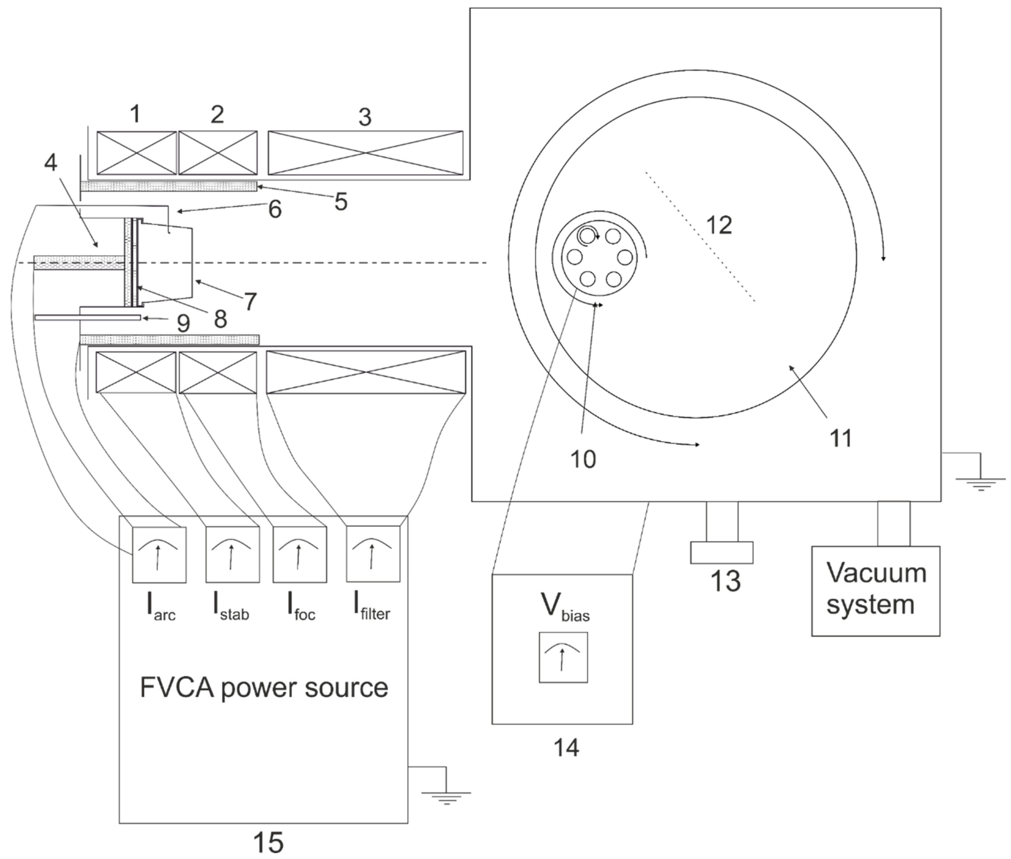
2. Materials and Methods

2.1. Cathode Production and Testing

The cathodes used were produced by three different companies: monolithic TiB2 (Plasma Technology Ltd., Hong Kong, China), TiB2-C (Plansee, Lechbruck, Germany) and TiB2-TiSi2 (Plasmaterials, Livermore, California). As materials other than metals require indirect cooling, a backplate had to be used to avoid direct contact between the cooling water and the cathode material. For the TiB2 and TiB2-TiSi2 cathodes, Cu backplates were used. The roughness of the TiB2-C material created additional thermal resistance at the interface between the cathode and backplate [20]; therefore, the TiB2-C was fastened to a Mo backplate with highly thermally conductive glue.

2.1.1. Cathode Testing

We used a filtered cathodic vacuum arc (FCVA) deposition system for the cathode testing and coating deposition. The system featured a cone-shaped cathode (67 mm × 50 mm and a 50-mm height), and the spot motion around the cathode was controlled by focusing and steering magnetic coils wrapped around the anode. An additional magnetic coil was used as a linear filter placed between the end of the anode and the substrate to minimise the number of macroparticles reaching the substrate. The power source allowed control of the arc current (up to 70 A), focusing coil (FcC) 3–7 A and filtering coil (FtC) 1–10 A, while the steering coil was fixed at 1 A. Prior to each test and deposition, the chamber pressure was pumped down to below 4 × 10⁻⁴ Pa.

Arc Spot Movement

The sample holder was removed, and a mirror was placed at 45° in the middle of the chamber to allow direct observation of the cathode during operation through the viewport. Each of the cathodes was tested, and parameters such as chamber pressure, Ar flow, magnetic field (coils current), and arc current were optimised to allow stable arc running after triggering and good spot mobility (fast motion in front of the cathode). The cathode fracture was assessed after arc running; fractured cathode parts were collected from around the anode, filter and chamber, and cathode height was measured.
To assess the influence of the magnetic field on the arc spot motion, the substrate holder presented in Figure 1 was replaced by an insulated metal plate (10 cm × 10 cm), and the electric potential between the plate and the ground was measured using a Versastat potentiostat. The data was collected for 60 s for each setting. We anticipated that, if we observed an arc running at the side of cathode and a high frequency of arc triggering, this would result in a lower potential generated by the ions hitting the metal plate, whereas stable arc running at the front face of the cathode would result in a higher potential generated at the plate.

Electrical Resistivity Measurements

Cathode parts that were removed after the initial arc-running tests were collected and used to measure the dependence of electrical resistivity on temperature. We assembled a special rig to do this, consisting of a Versastat potentiostat (Berwyn, USA), tube furnace and platinum wire (to limit the influence of oxidation on the measurement). Each cathode part was measured and placed on the ceramic base wrapped by platinum wires with 1 cm between them. To secure the part in place, additional nickel wires were used. The wires were connected to the Versastat potentiostat, allowing resistance measurements at regular intervals to be recorded in the computer. Before each measurement, the air was evacuated from the furnace using the rotary pump. An argon atmosphere was introduced with a flow of 200 sccm. The temperature was progressively increased from room temperature at a rate of 5 °C/min up to 1000 °C. DC current was applied to the sample, and the resistance was measured. For each cathode material, two samples were measured to ensure correct values. As the resistance (R) depends on the cross-section of the sample (s) and its length (l), the resistivity ( ρ ) was calculated based on Equation (1) to allow comparison between the samples:
ρ = R s l

2.2. Coating Deposition and Testing

2.2.1. Deposition Parameters

Silicon wafers, Kennametal EDCT milling inserts and Widia SUN120408 turning inserts were used as substrate materials. The substrate cleaning prior to each deposition included ultrasonic cleaning in an acetone bath for 15 min followed by rinsing in isopropyl alcohol. The substrates were then loaded on the rotating substrate holder, and the system was pumped down to below 4 × 10⁻⁴ Pa. The substrates were cleaned in situ by Ar etching; a negative 450 V bias was applied to the substrate for 10 min under a 13 Pa process pressure and a 100-sccm Ar flow.
The coating parameters for deposition on the cutting inserts were chosen based on initial cathode trials to ensure stable arc running (although, the arc running on the monolithic TiB2 cathode was too unstable to allow any coating deposition). The argon pressure was 4.5 × 10⁻³ Torr, the focusing coil current was equal to 5 A, the filtering coil was set to 10 A, and the substrates were grounded. For TiB2-C, the cathode arc current was set to 45 A, while, for TiB2-TiSi2, it was set to 50 A. The deposition time was 2 h.
To investigate the influence of bias, substrate pre-heating, and cathode cooling on coating thickness, another series of coatings was deposited on silicon samples partially covered by Kapton tape. Deposition parameters were kept as described above except for the time intervals. The step height was later measured using a Dektak profilometer (Billerica, USA). The possibility of cathode overheating during plasma generation was investigated. Therefore, the coating was deposited in fixed intervals: 5-min deposition intervals alternated with 5-min breaks (substrate temperature during this phase was maintained using the heater to avoid additional stress being generated in the coating) for 20-, 40- and 100-min total deposition times.

2.2.2. Machining Testing and Characterisation

To assess the potential of the coatings deposited on the new cathodes’ faces, we performed milling tests on an Okuma Cadet Mate CNC vertical machining centre (Oguchi, Japan). The cutting conditions are presented in Table 1 and were similar for both wet and dry machining tests. As the thickness of the deposited coatings was less than 1 µm, they were benchmarked not only to commercial TiB2-coated (2–3 µm) but also to thinner (1 µm) commercial TiAlN-coated and uncoated tools. An optical toolmaker microscope (Mitutoyo model TM, Takatsu, Japan) was used to measure and record the wear of the tool between passes.
A Tescan dual-beam focused ion beam scanning electron microscope (SEM) was employed to study the cross-sections of the coatings. A Philips SEM microscope (Amsterdam, Netherlands) equipped with energy-dispersive X-ray spectroscopy (EDX) (Abingdon, UK) detector was used to investigate the surface and chemical composition of cathodes, deposited coatings, chips collected during the machining and tools after use. The EDX also allowed us to explore the aluminium that had adhered to the tool, the area of which we later determined using ImageJ software. The cross-section images of the chips were obtained on an optical microscope. X-ray Powder Diffraction (XRD) (Amsterdam, Netherlands) has been employed to study the structure of the deposited coatings.
A Teer ST-3001 Tribo Tester was used to assess both friction coefficient (CoF) of deposited and benchmark coatings. The CoF was determined using a dry reciprocating sliding test with a fixed 5-mm WC ball drawn over the surface of the coating for a 10-mm distance for 100 cycles.
The hardness of deposited coatings and cathode material was determined using Micro Materials Ltd. Micro Materials NanoTest nanoindenter. The nanoindenter was calibrated against known quartz of SiO2 with the following data: hardness of 9 GPa, elastic modulus of 70 GPa and poison of 0.17. A series of 10 indents with a 100-mN load for cathodes and 25-mN for coatings was obtained, and an average value calculated.

3. Results

3.1. Cathode Material

3.1.1. Surface and Composition

The SEM images of the unused cathodes are presented in Figure 2. The grains of the monolithic TiB2 cathode had sharp edges, and the structure presented a high porosity. The sintering process did not result in a high-density cathode. The addition of C promoted reduction of oxides which typically inhibit surface mobility. Therefore, rounded grain boundaries can be observed due to improved surface mobility. In addition, carbon inclusions could be noticed at some of the grain boundaries. The surface morphology of the TiB2-TiSi2 cathode looked dense, and grains did not have sharp edges as they did in the monolithic TiB2, indicating the TiSi2 additive promoted the formation of liquid phase during the sintering process. The average grain size (7.3 µm) was smaller than that for TiB2-C (13.1 µm) but slightly larger than that for monolithic TiB2 cathode (5.6 µm). The chemical compositions of the cathodes and deposited coatings obtained using EDX are presented in Table 2. For all cathodes, the stoichiometric composition (B to Ti) 2:1 was achieved. The recognised carbon content for the TiB2-C cathode was around 13 at% and was lower than the Si content for TiB2-TiSi2, which was 5 at%. In addition, oxygen was present in this cathode at almost 20 at%, which was significantly higher than for the other two cathodes. The most probable reason for this is Si’s rapidly forming SiO2 while exposed to air.
The XRD analysis confirmed the formation of TiB2 phase in the coatings deposited from both of the cathodes as a low intensity TiB2(101) peak at approximate 2-theta angle of 44.5° could be detected. The further EDX analysis of the coatings indicated that the coating deposited from the TiB2-C cathode had TiB2 stochiometric composition. However, the oxygen and carbon contents were relatively higher than those in the cathode itself. Unlike the material of the TiB2-TiSi2 cathode, the deposited coating was TiB1.5 rather than TiB2. In addition, approximately 7 at% of Si is present in the coating structure.

3.1.2. Electrical Conductivity

The temperature dependence of electrical resistivity in the cathodes parts is presented in Figure 3. Resistivity at room temperature differed for each cathode material. The lowest resistivity was for TiB2-C, while monolithic TiB2 gave a significantly higher measurement. The density of the cathodes, as well as their composition (e.g., the good electrical conductivity of C), would have had a significant influence on these results. Although resistivity remained almost constant up to 100 °C, it increased almost linearly with increasing temperature for all of the cathodes. It is noticeable that the angle of the plot for monolithic TiB2 was significantly steeper (tanα = 5 × 10⁻⁶) than the plots for the other two cathodes (tanα = 1 × 10⁻⁶), confirming the influence of density on the electrical resistivity of TiB2.

3.1.3. Arc Stability

The initial arc-running tests involved parameter optimisation, arc observations and arc stability measurements (number of times the arc had to be triggered during 5 min). With the monolithic TiB2 cathode, it was not possible to trigger an arc with arc currents lower than 65 A (the power source maximum was 70 A). Even when triggered, the arc was not stable; the average time to next triggering was just 10 s. In addition, the TiB2 cathode arc tended to stick to a specific location on the cathode, leading to the extensive cathode fracture presented in Figure 4. Large cathode chunks could be seen especially in the anode but also around the filter. Arc paths could be observed on the side face of the monolithic TiB2 cathode after use.
By contrast, the TiB2-C cathode experienced exceptional arc stability—once triggered, the arc was running for the entire 5 min. The minimum current required to achieve a stable arc was 40 A, although it was possible to trigger an arc below that current level. During deposition, a constant flow of particles could be observed. These particles appeared to be cathode flakes and could be found in the filter and around the chamber after the deposition (Figure 4). The quantity of particles was significant and led to poor cathode utility; around 9 mm/hour was used, while the rate for the typical metallic cathode, e.g., Cr, is approximately 1–2 mm/h.
The TiB2-TiSi2 cathode required approximately 50 A arc current for stable deposition. The arc stability was good; arc-spot time was equal to 2 min. Contrary to the other two tested cathodes, multi-spot evaporation could be observed at times, which should have decreased the cathode fracturing, as it leads to a dissipation of the energy between two spots. Particle generation could be observed during arc running, and particles were later collected from the chamber bottom; however, they appeared to have solidified before reaching the substrate, as the resulting coatings were smooth. Some cathode fractures could be found in the anode and filter. However, the amount was significantly smaller than for monolithic TiB2, and no visible cathode fracture was observed.
The influence of the magnetic field from both focusing and filtering coils on the potential of generated plasma is presented in Figure 5a–d. These graphs also represent the overall stability and movement of the arc spot; when the arc was triggered frequently or tended to run along the side face of the cathode, the potential measured during acquisition time was lower.
Reference plots for a Cr cathode are provided (Figure 5a), as the Cr cathode was known from previous experiments on this setup to have exceptional arc movement and stability. It can be seen that, above the level of 3 A, an increase of the filter coil current (FtC) increased the measured potential, as the filter confined the plasma and more ions reached the metal plate. Similarly, an increase of the focusing coil current (FoC) increased the potential, as the arc was more focused on the front face of the cathode and the plasma was more confined. Interestingly, for the high FtC currents, there was little influence of the FoC.
The poor stability of the arc triggered on the monolithic TiB2 cathode, as ascertained by visual observations, was confirmed experimentally in Figure 5b. For an FoC set to 3 A, the arc rarely triggered, and, when it did so, it was running on the side face of the cathode, which resulted in low voltage measured. For higher FoC and FtC currents, the measured potentials were similar. Only an FtC current of 6–8 A with an FoC current at 6 A seemed to allow the arc to be sustained for a longer time at the front face of the cathode.
The influence of the magnetic field on the arc triggered on the TiB2-C cathode (Figure 5c) appeared to be similar to what had been seen with the Cr cathode, as all the lines followed an approximately linear pattern. For minimum settings of both FoC and FtC currents, the measured voltage was low (0.5 V), indicating an arc running at the side face of the cathode. However, once the FtC current reached 6–7 A, there was a rapid increase in the voltage measured, which indicated that the arc was running on the front face of the cathode. Overall, we noted that the filtering coil led to confinement of the plasma; therefore, the higher the FtC current was, the higher was the measured ion voltage. Similar behaviour could be observed with an increase in FoC current.
For the TiB2-TiSi2 cathode, the influence of the magnetic field (Figure 5d) was less noticeable than for TiB2-C and Cr. For FtC current values from 1 to 4 A and FoC current from 4 to 7 A, similar ion voltages were measured, indicating that the arc was running at the side face of the cathode. Once the FtC current was increased, the ion voltage varied. However, significantly higher values were achieved when FoC current was 6 to 7 A and FtC current was 6 to 9 A, indicating that such a magnetic field combination ensured good plasma confinement and arc running only at the front cathode face.

3.2. Coating Analysis

The TiB2 cathodes were used to deposit a series of coatings to assess their overall potential for replacing the commercial TiB2 coatings. The initial trials of 20 min of deposition produced coatings from both TiB2-C and TiB2-TiSi2 with a thickness of approximately 300 nm (Figure 6).
To obtain thicker coatings, a 2-h deposition was performed, including a study to determine the influence of a −100 V bias applied during deposition, defining whether it could provide better adhesion of the films and result in higher coating densities. Figure 7 presents the SEM images of deposited films. Despite the high particle generation observed from both TiB2-C and TiB2-TiSi2 cathodes, films produced appeared smooth, with average roughnesses (Ra) of 15 nm and 18 nm, respectively. Some particles with dimensions of 5–7 µm could be found on the samples, but they were rare. Despite increased deposition time, the thicknesses of the deposited films were only 500 nm for the TiB2-C cathode and 300 nm for the TiB2-TiSi2 cathode.
The coating produced with a −100 V bias had very low thickness (26 nm) and high roughness (Ra = 100 nm) compared to the other coatings. The coating SEM image appeared to be rough, with many particles on the surface of the coating.
The lower thickness than expected was potentially a result of possible overheating of the cathode. To confirm this effect, interval coating deposition tests with running periods of 5 min were carried out (as described in the ‘Experimental Procedure’ section), which should have allowed for maintaining a low temperature at the cathode. Three coatings were deposited using this method, with varied total deposition time. The results of 20-, 40- and 100-min deposition times were coatings with thicknesses of 200, 400 and 780 nm as presented in Table 3. Such results confirmed that a cathode overheating problem was a critical barrier that needs to be addressed.

3.2.1. Coefficient of Friction Measurements

The CoF measurements obtained from dry reciprocating sliding test under a 5-N load for 100 cycles on the produced and commercial TiB2 films are presented in Figure 8. For the sputtered TiB2 coating, a CoF of 0.26 was measured for the first 16 cycles, which increased to 0.4 by the time 100 cycles had been completed. Similar behaviour has been observed by other researchers [14,21] during short-length (100 µm) wear tests. They found that the running-in period lasted for around 3000 cycles, until a steady-state value of approximately 0.8 was achieved. By contrast, both arc-deposited TiB2 coatings from TiB2-C and TiB2-TiSi2 cathodes adapted during the first 15 cycles, at which point they achieved steady CoFs of 0.43 and 0.47, respectively.

3.2.2. Hardness

Nanoindentation allowed the hardness values of cathode materials and coatings to be measured. The highest value for cathode hardness (Figure 9) was obtained for monolithic TiB2 and was ±24 GPa. The cathodes with C and TiSi2 additions displayed slightly lower hardness of ±23 GPa, which is however within the error limit. The TiB2-C coating produced (Figure 10) a slightly harder coating (~21.1 GPa) than that of TiB2-TiSi2; however, the standard deviation of the indents was also greater. By contrast, the coating from the TiB2-TiSi2 cathode displayed a lower hardness value (~16.4 GPa), although it was still within the acceptable range, considering no coating optimisation (e.g., interlayer or substrate heating) had been applied.

3.2.3. Machining

In the wear process, three stages can typically be identified: the running-in stage, the steady state and the surface-damage stage. The initial stage allows the tool-machined part adaptation process, and, therefore, it is typically associated with increased wear, while, once the tool reaches the surface-damage stage, it has to be replaced [22]. In the middle, steady-state, stable tool wear, and friction are achieved, therefore, the tool wear is restricted. To reduce tool wear, it is necessary to have a rapid tool adaptation that results in a prolonged steady-state stage. Such conditions result in better machined-surface finish and tool-life enhancement [22,23]. Figure 11 shows a comparison of the change in flank wear of uncoated, TiB2-coated, and TiAlN-coated inserts in terms of cutting length during AlSi milling with coolant. Up to ±18 m of machining, the lowest amount of tool wear, was observed for the TiAlN coating. This coating experienced a running-in stage for the first 5 m, then a stable state started and continued up to 8 m, after which elevated tool wear could be observed. The uncoated tool, by contrast, experienced constant wear through 25 m of machining, after which the wear speed decreased significantly, indicating the tool was in the stable state, which continued until the machining process was stopped at 30 m. A similar path was followed by both the commercial TiB2 tool and the tool coated from the TiB2-TiSi2 cathode. TiB2-C, however, allowed significantly faster tool adaptation, as the stable state could be observed after 12 m of machining, while the tool wear was lower than for the uncoated tool.
The uncoated and coated tools from these trials were also tested during dry AlSi machining as a way to represent the most extreme conditions. The wear curves are presented in Figure 12. In dry machining, in the absence of a lubricant, the coating serves as a source of lubrication, thus significantly higher wear is expected. Commercial TiB2 experienced elevated wear during the running-in stage, after which no increase in wear was observed up to 5 m. Thereafter, steady tool wear could be seen until wear reached 300 µm, when machining was stopped. The TiAlN-coated tool followed a wear curve similar to that of commercial TiB2. However, the tool wear in the adaptation phase (first 3 m) was lower, and, then, rather than going into the stable state, the tool experienced significantly lower wear up to 10 m, after which the wear progressed quickly until the cutting process was stopped at 25 m of total machining length. The adaptation phase for uncoated and TiB2-coated tools baths required approximately 2 m of machining as well; however, the stable state continued up to 8 m. This phase was followed by elevated tool wear, although periodic (e.g., for TiB2-C from 8–12 m and 14–16 m) stable states were observed.

3.2.4. Tool Investigation

Figure 13 and Figure 14 present the SEM micrographs and EDX elemental analysis (Al represented in green) of the rake surfaces of the worn tools after wet and dry Al-10Si machining. The area covered by Al was calculated using ImageJ software, and the values added to the images. Al adhering to the rake edge could be noticed for all of the samples in Figure 13; it was concentrated close to the tool edge, and no aluminium was observed at the flank face. The amount of Al differed by tool; the highest could be seen for commercial TiB2, the lowest for uncoated and TiB2-TiSi2-coated tools.
The rake faces of the tools after dry machining differed significantly from those rake faces used in the presence of a lubricant. Extensive BUE could be observed on all the tools tested (Figure 14). Chipping could be noticed for the uncoated tool and for TiB2-C, while slightly less was seen for TiAlN and TiB2-TiSi2. The uncoated tool had the greatest amount of adhered Al, forming a thick layer on both rake and flank faces. In appearance, the smallest amount of BUE was present on the TiB2-TiSi2 sample, although the area covered was slightly larger than that for TiB2-C.

3.2.5. Chip Comparison

Analysis of the chips resulting from machining with TiAlN and TiB2-C-coated tools indicated that those tools had the greatest and the least flank wear, respectively, after 30 m of wet AlSi machining. Optical images of the chip cross section displaying the chip microstructure as well as a secondary electron image of the under surface are presented in Figure 15. Systematic chip segmentation could be recognised on the chip under surface produced with the TiB2-C coated tool, confirming that good chip-tool lubrication [24] was provided; therefore, continuous chip flow had taken place. By contrast, although some chip segments could be recognised on the chip produced with TiAlN coated tool, those segments were irregular, which indicated that the chip flow was not continuous and no plastic deformation had occurred [25].
The microstructure and under the surface of the chips obtained from dry machining with uncoated, TiB2 and TiB2-TiSi2 coated tools are presented in Figure 16. Regular segments could be observed on all of the chips. However, the segments from the uncoated tool were several times larger than those from other tools. Such chips can be observed when ploughing action takes place instead of cutting, as lubrication is not provided [1,26,27]. Lack of lubrication on uncoated tools resulting in limited plastic deformation could be observed on the chip microstructure as well; many of the grains were undeformed. On the other hand, grain elongation typically associated with good chip-tool area lubrication [24,28], which improves chip flow speed, was observed on chips from both TiB2 and TiB2-C.

4. Discussion

4.1. Cathode Material

4.1.1. Monolithic TiB2

The measured hardness of the unused cathode material is equal to 24 GPa and is consistent with previous observations [4]. However, the grain structure observed on SEM micrograph (Figure 2) indicated that sintering in the liquid phase was not achieved, as mostly sharp grain edges are present. No sinter additives that could promote liquid-phase sintering [14] were used; therefore, considering the low self-diffusion coefficient of TiB2, which makes it difficult to densify [5], high density was not achieved. The electrical resistivity of this cathode (Figure 3) at room temperature is significantly higher than for the other cathodes produced in this work, and it grows more quickly with increasing temperature. This observation matches the results of other researchers [12] who studied the influence of the structure and density of TiB2 on its resistivity. They concluded that good densification could decrease the effect of increasing temperature on TiB2 resistivity. The high temperatures created by the arc can locally melt TiB2 [10], leading to its densification. Zhircov et al. [9] proposed that, if the density of the virgin cathode was not high, this local densified cathode area could have significantly lower electrical resistivity. The specific arc motion depends on a variety of factors (magnetic fields, local impurities, phases) [29]; however, the increased conductivity caused by densification can lead to the arc spot sticking to a specific location on the TiB2 cathode. Such behaviour was observed when running the arc on the produced monolithic TiB2 cathode; observations by eye confirmed that the arc was sticking to a particular location. In addition, a very high (compared to other cathodes) arc current (65 A) was required to trigger the arc. The need for high arc current confirms lower electrical conductivity, which correspondingly resulted in poor arc stability and significant cathode fracture (Figure 4) caused by high local temperature (more energy carried by the arc spot). The dependence of the thermal expansion coefficient of boride on its temperature can be considered as one of the main reasons for the cathode destruction [4].
Cathode spots can move randomly around the cathode, and spot motion has to be controlled to prevent erosion of supporting structures [30]. The spot motion can be restricted by insulating shields; however, much more definitive control can be ensured only by applying a magnetic field [20]. Typically in industry, a racetrack configuration is used with an arched circular field produced by a magnetic coil [31] or permanent magnet [32]. Previous studies [10] suggested, however, that, in the case of arc evaporation of TiB2, the removal of the magnetic field can decrease cathode fracturing by preventing overheating of a certain area (circular race track) on the cathode [33]. Zharkov et al. [9] completely removed the magnetic field, which resulted in a stable and reproducible plasma generation. For the cone-shaped cathode used in this work, the focusing coil applies an axial magnetic field that focuses the arc spot on the front face of the cathode [34]. The filter coil is used mainly to confine the plasma and guide it towards the substrate, but it also influences the arc spot [35]. As the fields coexist, their elimination would result in arc stability problems and spot movement mostly on the side face (where it is triggered) [20,30]. This concept is confirmed by ion voltage measurements on a Cr cathode. When the minimum coil current settings allowed in this system are used, the measured voltage is very low. In addition, the magnetic field of the focusing coil has the greatest influence on the average ion voltage, and above 6 A of FtC current, the effect of the FoC is limited. For these reasons, limiting the magnetic field when using a monolithic TiB2 cathode does not improve arc stability, as it did for other researchers [9,10]. In fact, for FoC, arc triggering is almost impossible. For the highest FoC and FtC currents, the arc is triggered but its high instability throughout the range of currents is the main influence on the measured ion voltage.

4.1.2. TiB2-C

The TiB2-C produced cathode has a well-densified structure (99.9% TD according to the manufacturer specification); however, the grains are larger than for the other cathodes. To achieve good densification without using sintering additives, temperatures above (2000 °C) were used. Extensive grain growth at high temperatures has been reported before and is typical for boride materials [36,37]. The good densification of the cathode resulted in higher room-temperature conductivity (compared to the other cathodes produced) and significantly lower dependence of conductivity on temperature. In addition, the hardness of the virgin cathode is found to be close to that of monolithic TiB2, indicating that the addition of C did not have a negative effect on the mechanical properties. The arc stability was substantially improved over the monolithic TiB2; the minimum arc current needed was just 40 A, and optical observations confirmed good arc mobility. For low FoC and FtC currents, the arc tends to run on the side face of the cathode, resulting in low measured ion voltage. However, increasing currents of both the FoC and the FtC increases the measured ion voltage, and ion voltage is greatest when both of these coils are set to their maximum values. We noticed that an FtC current of 4–5 A is required to confine the plasma to the metal plate used for measurement, as increasing the FoC current above this level results in a significant increase of measured ion voltage.
Densification and the addition of C lead to arc stability. The carbon inclusions locate around TiB2 crystals and, having better stress resistance, can serve as stopping points for propagating cracks [38,39], although this does not stop completely the destruction of the cathode during arc operation. As evidence of this, constant generation of cathode flakes could be observed when running the arc, no matter what parameters were used. The flakes could be found everywhere around the chamber, though their highest concentration was in the anode and filter tubes. Possibly, the flakes are created as follows: a crack forms and propagates at the cathode surface because of the thermal shock created by the arc spot; however, it stops at the carbon inclusion [31]. Due to explosive nature of the arc spot [40], a weakly attached flake is released, the spot moves to a different location, and the process repeats. This constant generation of flakes is also the reason for exceptional stability of the arc on this particular cathode, as the tiny volume of the material affected (melted) by the arc is being constantly removed; therefore, the spot is pushed to start at the new, virgin location. Although the arc movement and stability are improved, the utilisation of the cathode as a result of flaking is poor, with approximately 9 mm of the cathode being consumed per hour. The same cathode (same composition and manufacturer) was used by Zhircov et al. [9] in their work; they, however, do not describe such high cathode consumption. The high cathode consumption in our work may be due to the different arc source configuration used (i.e., a cone-shaped cathode). Zhircov et al. used the typical racetrack cathode equipped with a protective stainless steel ring [9], which possibly limited wear. In addition, better cathode cooling could be ensured, as their cathode is thinner than the cone-shaped one.

4.1.3. TiB2-TiSi2

The grain structure of TiB2-TiSi2 indicates good densification, and no extensive grain growth can be observed. The electrical resistivity at room temperature is slightly higher than that observed with the TiB2-C cathode. However, resistivity does grow with increasing temperature in a manner similar to that of TiB2-C, confirming good densification [12]. TiSi2’s phase is liquid at temperatures below 1700 °C; therefore, it can wet TiB2 [18]. Despite TiSi2 having a lower hardness (8–10 GPa) [41], its addition did not affect the hardness of the TiB2-TiSi2, and a hardness of 23 GPa was measured, which is close to the hardness of monolithic TiB2 (24 GPa). Arc stability and mobility are improved over those seen with monolithic TiB2, and the minimum arc current required is 50 A. Unlike other cathodes tested, multi-spot evaporation (many small spots distributed over a larger area) can be observed. This behaviour is typically observed on poisoned cathodes (deposition in a reactive gas atmosphere), as the ion bombardment charges the contaminants, thereby creating an electric field that enhances emission of electrons [30]. The rate of charging and the field enhancement and emission onset are very fast, and several emission centres switch on simultaneously [9]. TiSi2 crystals can serve as ‘contaminants’, the energy per spot is reduced, and a more extensive area is heated by the arc current. As a result, local overheating is reduced, which stabilizes the arc and limits the thermal shock, which in turn limits cathode cracking [30].
The high abundance of particles seen during the arc evaporation is typically associated with a material having a low melting point [30]. Since TiB2 has a high melting point (~3500 K) [37], it is expected to produce an insignificant number of droplets. However, once the arc is triggered, extensive particle emission can be observed visually as a glowing spark, and these are also found around the chamber after deposition. Similar observations of intense emission of visible droplets have been reported by other researchers [9,10]. Another mechanism for particle generation from materials with a high melting point has been proposed, one that differs from the generally accepted mechanism that is based on the presence of a molten bath and varied plasma pressure [30]. Given the high degree of flaking of the TiB2-C cathode, we can suggest that particles are produced due to the constant destruction of the thin surface layer of the cathode caused by explosive nature of the arc spot. The layers are smoothed by the high temperature of the arc. As a result, new crystals can be accessed, which decreases the chance that the spot will be immobilised at a single location.
The ion voltage measurements indicate that the stable arc running at the front face can be achieved, although it requires a certain distribution of the magnetic field generated by filtering and focusing coils. Similar to the TiB2-C cathode, for FtC currents below 4–5 A, low ion voltage is measured. The optimum currents appear to be an FtC of 8–9 A and an FoC of 6–7 A.

4.2. Analysis of Deposited Coatings

There is no reflection of the intensive flux of glowing particles on the film surfaces. As expected, most of those particles are solid and too big for possible attachment. The film surfaces are smooth, with roughness Ra = 15–18 nm, and only a few droplets are measured. The stoichiometric composition of the coating produced using the TiB2-C cathode is close to that of monolithic TiB2, and the measured hardness of the produced coating of around 21 GPa confirms the addition of C did not deteriorate mechanical properties of the TiB2. For the TiB2-TiSi2 cathode, the depletion of B can be observed and may be explained by the previously shown dependence of spatial plasma distribution on ion mass [9]. It is known that lighter elements typically have a wider distribution, and a reduced intensity along the cathode normal can be expected for lighter ions as compared to heavier elements [42]. This is consistent with the observed reduction of B, compared with Ti, in a film. The lower B content results in lower hardness (16.4 GPa) compared to TiB2-C obtained for this coating. Those hardness values are relatively lower than the hardness reported in other works using the magnetron sputtering technique, which are typically in the 30–50 GPa range [3,6,8,43]. As reported by other researchers, the hardness of TiB2 coating strongly depends on the residual stress, which results from the combination of deposition temperature, preferred crystal orientation, and substrate bias [3]. In addition, in the case of the deposition using FCVA, a small fraction of macro particles would be incorporated into the coating affecting the measured hardness [5].
Even though the 30–50 GPa hardness range of the TiB2 coatings deposited was not achieved, the measured hardness is still high and can be considered as a success, since it was obtained for the very first coating deposited from the cathode with novel composition. An optimisation of the coating deposition parameters to achieve hardness comparable with the one reported for magnetron sputtering is outside the scope of this article.
When used for wet machining, both coatings provide good lubrication and decrease tool wear. In fact, TiB2-C seems to achieve a steady steady-state after 13 m and shows little wear increase up to 30 m, exceeding all other coatings tested. In the absence of a lubricant, higher temperatures are achieved, and the coating serves as a source of lubrication [44]. As the thickness of deposited films from our cathodes was lower than 1 µm, they were not able to prevent tool wear. Extensive built-up edge occurred, which can be observed on EDX element maps. Although BUE is undesirable, it can serve as a protective layer that detaches once reaching a certain size [9]. The BUE growth can be observed on the plot as a flat segment that rapidly increases once the BUE detaches.
The initial trials on grounded samples indicated the deposition rate should be equal to 900 nm/h. However, when the deposition time was raised, it resulted in coatings having just 300 nm and just 26 nm for the biased sample. Application of bias increases the energy of the ions. Therefore, higher compressive stress is introduced in the coating [45]. Treglio et al. [11] reported that a −75 V bias applied during pulsed arc TiB2 deposition leads to fracture and flaking of the coating, which becomes thin and rough. The high roughness of the coating deposited with a −100 V bias in our work supports this conclusion. When a range of bias voltages from 0 to −100 V was applied during a 5-min deposition of thin film, no difference in thickness was observed, confirming that at least a certain thickness has to be achieved to cause coating destruction by compressive stress [11]. As for the grounded substrates, Knotek et al. [10] and Zhirkov et al. [9] do not report observing thickness limitation, although they also do not report their actual coating thicknesses.
The following parameters were considered as potentially contributing to the unexpectedly thin coatings: low thermal conductivity of TiB2 (25 W/m*K); greater length of the cathode compared to racetrack configurations; indirect cooling, consequently, an interface with a certain thermal resistance was created between the cathode and Cu backplate. Considering these, we propose cathode overheating as the primary reason for the low thickness of the resulting coatings. Only 10% of the arc current is transformed into the ion energy [30], while the rest is used to heat the cathode. In case of an insufficient cathode cooling rate, the front face of the cathode becomes seriously overheated, which leads to an increase in electrical resistivity (see Section 3.1.2 Electrical conductivity), which in turn increases the temperature even further. Such behaviour can increase the number of droplets being produced, and, as it was found, these droplets solidify before reaching the substrate rather than becoming part of it, and coating deposition rate decreases drastically. The solution we proposed in this paper was to preheat the substrate before deposition to 200 °C (the maximum for the system) and to perform deposition in 5-min evaporation steps, leaving 5-min breaks to cool down the cathode (with the substrate temperature being maintained by heaters to avoid coating stress). This method allowed us to successfully deposit a 780-nm-thick film during 100 min total evaporation time. Our method was proof-of-concept and indicated that good cathode cooling is essential for TiB2-coating deposition. In the case of this system configuration with cone-shaped cathodes, higher-flow, very-low-temperature coolant should be used, and the height of the cathode could be decreased to limit the thermal gradient.

5. Conclusions

We evaluated the use of TiB2 for arc evaporation after first densifying its structure and adding non-metallic sinter additives such as C and TiSi2. We successfully tested a cylindrical cone-shaped cathode configuration and compared its attributes to those of monolithic TiB2 cathodes:
  • The additives did not significantly affect the material hardness. All of the cathodes produced have a bulk hardness of 23–24 GPa.
  • Arc was difficult to trigger in monolithic TiB2 cathode and required high arc currents of 65 A because of the lower electrical conductivity. Arc spots were found to stick at certain locations due to densification of the area at the arc spot, leading to extensive local fracturing of the cathode.
  • We found that TiB2-C required the lowest current setting (40 A) to trigger an arc and provided the best arc-spot stability and mobility. Carbon inclusions successfully prevented crack propagation, although they did not stop crack initiation, which resulted in high cathode flaking and poor target utilisation.
  • Good densification of both TiB2-C and TiB2-TiSi2 cathodes limits the influence of temperature on the conductivity of the cathode material. High density was identified as the main reason for significantly better arc stability and lower arc currents required for those cathodes in comparison to monolithic TiB2. We observed multi-arc evaporation when operating a TiB2-TiSi2 cathode and found it decreases the fracturing of the cathode. The currents required to trigger a TiB2-TiSi2 cathode are slightly higher (50 A) than for TiB2-C.
  • Contrary to previous reports about arc evaporation of TiB2, appropriate distribution of magnetic fields from filtering and focusing coils was found to be essential for maintaining stable and mobile arc spots on TiB2-C and TiB2-TiSi2 cathodes.
We have used the produced TiB2 cathodes to deposit thin films on the cutting tools. Following observations were made:
  • Only TiB2-C and TiB2-TiSi2 provided arc stability allowing deposition of coatings on the cutting tools. Despite an intense flux of microparticles, the deposited films are smooth with Ra = 15–18 nm, indicating that the droplets solidify before reaching the substrates.
  • TiB2-C cathode produced films with TiB2 stochiometric composition and hardness comparable to the commercial TiB2.
  • Flank wear assessment during AlSi machining revealed that this TiB2-C coating provides better protection against abrasive wear than a commercial coating over the course of 35 m of machining.
  • The deposition from TiB2-TiSi2 resulted in coatings that have a TiB1.5 composition most likely due to the dependence of spatial plasma distribution on ion mass. This depletion of boron results in lower measured hardness. However, the machining tests showed good wear protection, resulting in decreased tool wear.
  • We also found that overheating leads to extensive particle generation, which significantly decreases the deposition rate. Deposition in 5-min steps allowed deposition of 780 nm-thick films, indicating that coating cathode temperature has to be controlled and kept low.

Author Contributions

Methodology, G.S.F.R.; investigation, T.L.B. and J.M.P.; conceptualization, I.A.; resources, J.K. and S.C.V.; writing—original draft preparation, T.L.B.; writing—review and editing, J.R.; visualization, T.L.B.; supervision, J.L.E.; project administration, J.L.E.; funding acquisition, J.K. All authors have read and agreed to the published version of the manuscript.

Funding

This research was partially funded by Kennametal Gmbh.

Acknowledgments

The authors would like to acknowledge Peter Polcik (Plansee Gmbh) for his advice and supplying additional TiB2-C cathode for testing. Financial support from the Basque Government Industry Department under the ELKARTEK program (project acronym: INTOOL1) is also gratefully acknowledged.

Conflicts of Interest

The authors declare no conflict of interest.

References

  1. Said, M.S.; Ghani, J.A.; Che Hassan, C.H.; Shukor, J.A.; Selamat, M.A.; Othman, R. Chip Formation in the Machining of Al-Si/10% AlN Metal Matrix Composite by using a TiN-coated Carbide Tool. Res. J. Appl. Sci. Eng. Technol. 2016, 13, 422–426. [Google Scholar] [CrossRef]
  2. Roy, P.; Sarangi, S.K.; Ghosh, A.; Chattopadhyay, A.K. Machinability study of pure aluminium and Al-12% Si alloys against uncoated and coated carbide inserts. Int. J. Refract. Met. Hard Mater. 2009, 27, 535–544. [Google Scholar] [CrossRef]
  3. Mikula, M.; Grančič, B.; Buršíková, V.; Csuba, A.; Držík, M.; Kavecký, Š.; Plecenik, A.; Kúš, P. Mechanical properties of superhard TiB2 coatings prepared by DC magnetron sputtering. Vacuum 2007, 82, 278–281. [Google Scholar] [CrossRef]
  4. Munro, R.G. Material properties of titanium diboride. J. Res. Natl. Inst. Stand. Technol. 2000, 105, 709. [Google Scholar] [CrossRef]
  5. Basu, B.; Raju, G.B.; Suri, A.K. Processing and properties of monolithic TiB2 based materials. Int. Mater. Rev. 2006, 51, 352–374. [Google Scholar] [CrossRef]
  6. Berger, M.; Larsson, M.; Hogmark, S. Evaluation of magnetron-sputtered TiB2 intended for tribological applications. Surf. Coat. Technol. 2000, 124, 253–261. [Google Scholar] [CrossRef]
  7. Chowdhury, M.S.I.; Chowdhury, S.; Yamamoto, K.; Beake, B.D.; Bose, B.; El, A.; Cavelli, D.; Dosbaeva, G.; Aramesh, M.; Fox-rabinovich, G.S.; et al. Wear behaviour of coated carbide tools during machining of Ti6Al4V aerospace alloy associated with strong built up edge formation. Surf. Coat. Technol. 2017, 313, 319–327. [Google Scholar] [CrossRef]
  8. Grančič, B.; Mikula, M.; Hrubá, L.; Gregor, M.; Štefečka, M.; Csuba, A.; Dobročka, E.; Plecenik, A.; Kúš, P. The influence of deposition parameters on TiB2 thin films prepared by DC magnetron sputtering. Vacuum 2005, 80, 174–177. [Google Scholar] [CrossRef]
  9. Zhirkov, I.; Petruhins, A.; Naslund, L.A.; Kolozsvári, S.; Polcik, P.; Rosen, J. Vacuum arc plasma generation and thin film deposition from a TiB2 cathode. Appl. Phys. Lett. 2015, 107. [Google Scholar] [CrossRef] [Green Version]
  10. Knotek, O.; Loffler, F.; Bohmer, M.; Breidenbach, R.; Stobel, C. Ceramic cathodes for arc-physical vapour deposition: Development and application. Surf. Coat. Technol. 1991, 49, 263–267. [Google Scholar] [CrossRef]
  11. Treglio, J.R.; Trujillo, S.; Perry, A.J. Deposition of TiB2 at low temperature with low residual stress by a vacuum arc plasma source. Surf. Coat. Technol. 1993, 61, 315–319. [Google Scholar] [CrossRef]
  12. McLeod, A.D.; Haggerty, J.S. Electrical Resistivities of Monocrystalline and Polycrystalline TiB2. J. Am. Ceram. Soc. 1984, 67, 705–708. [Google Scholar] [CrossRef]
  13. Zhirkov, I.; Kolozsvári, S.; Polcik, P.; Rosen, J. Vacuum arc plasma generation and thin film synthesis from a TiB2 cathode. In Proceedings of the Process Systems Engineering, Linkoping, Sweden, 2 November 2015. [Google Scholar]
  14. Murthy, T.S.R.C.; Basu, B.; Srivastava, A.; Balasubramaniam, R.; Suri, A.K. Tribological properties of TiB2 and TiB2—MoSi2 ceramic composites. J. Eur. Ceram. Soc. 2006, 26, 1293–1300. [Google Scholar] [CrossRef]
  15. Schultes, G.; Schmitt, M.; Goettel, D.; Freitag-Weber, O. Strain sensitivity of TiB2, TiB2, TaSi2 and WSi2 thin films as possible candidates for high temperature strain gauges. Sens. Actuators A Phys. 2006, 126, 287–291. [Google Scholar] [CrossRef]
  16. Murthy, T.S.R.C.; Basu, B.; Balasubramaniam, R.; Suri, A.K.; Subramanian, C.; Fotedar, R.K. Processing and properties of TiB2 with MoSi2 sinter-additive: A first report. J. Am. Ceram. Soc. 2006, 89, 131–138. [Google Scholar] [CrossRef]
  17. Murthy, T.S.R.C.; Subramanian, C.; Fotedar, R.K.; Gonal, M.R.; Sengupta, P.; Kumar, S.; Suri, A.K. Preparation and property evaluation of TiB2 + TiSi2 composite. Int. J. Refract. Met. Hard Mater. 2009, 27, 629–636. [Google Scholar] [CrossRef]
  18. Biswas, K.; Basu, B.; Suri, A.K.; Chattopadhyay, K. A TEM study on TiB2—20%MoSi2 composite: Microstructure development and densification mechanism. Scr. Mater. 2006, 54, 1363–1368. [Google Scholar] [CrossRef]
  19. Murthy, T.S.R.C.; Sonber, J.K.; Subramanian, C.; Hubli, R.C.; Suri, A.K. Densification, characterization and oxidation studies of TiB2—WSi2 composite. Int. J. Refract. Met. Hard Mater. 2012, 33, 10–21. [Google Scholar] [CrossRef]
  20. Boxman, R.L.; Zhitomirsky, V.N. Vacuum arc deposition devices. Rev. Sci. Instrum. 2006, 77, 021101. [Google Scholar] [CrossRef]
  21. Prakash, B.; Ftikos, C.; Celis, J.P. Fretting wear behavior of PVD TiB2 coatings. Surf. Coatings Technol. 2002, 154, 182–188. [Google Scholar] [CrossRef]
  22. Fox-Rabinovich, G.; Totten, G.E. Self-Organization During Friction: Advanced Surface-Engineered Materials and Systems Design; CRC Press: Boca Raton, FL, USA, 2013; Volume 53. [Google Scholar]
  23. List, G.; Nouari, M.; Géhin, D.; Gomez, S.; Manaud, J.P.; Le Petitcorps, Y.; Girot, F. Wear behaviour of cemented carbide tools in dry machining of aluminium alloy. Wear 2005, 259, 1177–1189. [Google Scholar] [CrossRef]
  24. Ahmed, Y.S.; Veldhuis, S.C. The study of wear performance and chip formation of coated carbide tools during machining super duplex stainless steels. In Proceedings of the 6th International Conference Virtual Machining Process Technology, Montreal, Canada, 29 May–2 June 2017. [Google Scholar]
  25. Kishawy, H.A.; Dumitrescu, M.; Ng, E.G.; Elbestawi, M.A. Effect of coolant strategy on tool performance, chip morphology and surface quality during high-speed machining of A356 aluminum alloy. Int. J. Mach. Tools Manuf. 2005, 45, 219–227. [Google Scholar] [CrossRef]
  26. Ning, L.; Veldhuis, S.C.; Yamamoto, K. Investigation of wear behavior and chip formation for cutting tools with nano-multilayered TiAlCrN/NbN PVD coating. Int. J. Mach. Tools Manuf. 2008, 48, 656–665. [Google Scholar] [CrossRef]
  27. König, W.; Fritsch, R. Physically vapor deposited coatings on cermets: Performance and wear phenomena in interrupted cutting. Surf. Coatings Technol. 1994, 68–69, 747–754. [Google Scholar] [CrossRef]
  28. Joshi, S.; Tewari, A.; Joshi, S. Influence of Preheating on Chip Segmentation and Microstructure in Orthogonal Machining of Ti6Al4V. J. Manuf. Sci. Eng. 2013, 135, 061017. [Google Scholar] [CrossRef]
  29. Anders, A. The fractal nature of vacuum arc cathode spots. IEEE Trans. Plasma Sci. 2005, 33, 1456–1464. [Google Scholar] [CrossRef] [Green Version]
  30. Anders, A. Cathodic Arcs Fom Fractal Spots to Energetic Condensation; Springer Inc.: New York, NY, USA, 2008. [Google Scholar]
  31. Kaplan, L.; Zhitomirsky, V.N.; Goldsmith, S.; Boxman, R.L.; Rusman, I. Arc behaviour during filtered vacuum arc deposition of Sn-O thin films. Surf. Coat. Technol. 1995, 76–77, 181–189. [Google Scholar] [CrossRef]
  32. Davy, S.H. Handbook of Vacuum Arc Science and Technology. Handb. Vac. Arc Sci. Technol. 1996, 709–736. [Google Scholar]
  33. Zhirkov, I.; Petruhins, A.; Rosen, J. Effect of cathode composition and nitrogen pressure on macroparticle generation and type of arc discharge in a DC arc source with Ti-Al compound cathodes. Surf. Coatings Technol. 2015, 281, 20–26. [Google Scholar] [CrossRef]
  34. Jütner, B. Characterization of the cathode spot. IEEE Trans. Plasma Sci. 1987, 15, 474–480. [Google Scholar] [CrossRef]
  35. Aksyonov, D.S.; Aksenov, I.I.; Zadneprovsky, Y.A.; Loboda, A.M.; Mel, S.I.; Shulayev, V.M. Vacuum-Arc Plasma Source with Steered Cathode Spot. Probl. At. Sci. Technol. Phys. 2008, 210–212. [Google Scholar]
  36. Demirskyi, D.; Sakka, Y. High-temperature reaction consolidation of TaC-TiB2 ceramic composites by spark-plasma sintering. J. Eur. Ceram. Soc. 2015, 35, 405–410. [Google Scholar] [CrossRef]
  37. Balcı, Ö.; Burkhardt, U.; Schmidt, M.; Hennicke, J.; Barış Yağcı, M.; Somer, M. Densification, microstructure and properties of TiB2 ceramics fabricated by spark plasma sintering. Mater. Charact. 2018, 145, 435–443. [Google Scholar] [CrossRef]
  38. O’sullivan, M. Plansee Composite Materials GMBH Titanium Diboride Target. U.S. Patent No. 9,481,925, 1 November 2016. [Google Scholar]
  39. Polcik, P.; Franzke, E.; Wolff, M. Plansee Composite Materials GMBH Conductive Target Material. U.S. Patent Application No. 14/917,094, 2016. [Google Scholar]
  40. Liu, H.; Li, L.; Gu, J.; Wang, Q.; Huang, K.; Xu, Y. Research on unusual cathode erosion patterns in the process of filtered cathodic vacuum arc deposition. Int. J. Adv. Manuf. Technol. 2018, 96, 1779–1785. [Google Scholar] [CrossRef]
  41. Murthy, T.S.R.C.; Sonber, J.K.; Sairam, K.; Bedse, R.D.; Chakarvartty, J.K. Development of Refractory and Rare Earth Metal Borides & Carbides for High Temperature Applications. Mater. Today Proc. 2016, 3, 3104–3113. [Google Scholar]
  42. Nikolaev, A.G.; Yushkov, G.Y.; Savkin, K.P.; Oks, E.M. Angular distribution of ions in a vacuum arc plasma with single-element and composite cathodes. IEEE Trans. Plasma Sci. 2013, 41, 1923–1928. [Google Scholar] [CrossRef]
  43. Mikula, M.; Grančič, B.; Roch, T.; Plecenik, T.; Vávra, I.; Dobročka, E.; Šatka, A.; Buršíková, V.; Držík, M.; Zahoran, M.; et al. The influence of low-energy ion bombardment on the microstructure development and mechanical properties of TiB2 coatings. Vacuum 2011, 85, 866–870. [Google Scholar] [CrossRef]
  44. Jianxin, D.; Tongkun, C.; Lili, L. Self-lubricating behaviors of Al2O3/TiB2 ceramic tools in dry high-speed machining of hardened steel. J. Eur. Ceram. Soc. 2005, 25, 1073–1079. [Google Scholar] [CrossRef]
  45. Anders, A. A review comparing cathodic arcs and high power impulse magnetron sputtering (HiPIMS). Surf. Coat. Technol. 2014, 257, 308–325. [Google Scholar] [CrossRef] [Green Version]
Figure 1. Schematic view of the filtered cathodic vacuum arc (FCVA) deposition system (1—stabilising coil, 2—focusing coil, 3—filtering coil, 4—cooling pipe, 5—anode, 6—trigger, 7—cathode, 8—, 9—argon inlet,10—rotating substrate holder, 11—substrate table, 12—mirror, 13—viewport, 14—substrate bias power unit, 15—FVCA power source).
Coatings 10 00244 g001
Figure 2. SEM images of the virgin cathode surface.
Coatings 10 00244 g002
Figure 3. Electrical resistivity dependence on temperature of produced TiB2 cathodes.
Coatings 10 00244 g003
Figure 4. Comparison of the cathodes and fractured material in the filter after 60 min of arc running.
Coatings 10 00244 g004
Figure 5. Ion voltage measured for different electric currents of focusing and filter coils for (a) Cr, (b) monolithic TiB2, (c) TiB2-C, (d) TiB2-TiSi2 cathodes.
Coatings 10 00244 g005
Figure 6. SEM cross-sectional image of TiB2 coating deposited from TiB2-C cathode.
Coatings 10 00244 g006
Figure 7. SEM images of coatings deposited from different cathodes for two hours of deposition time.
Coatings 10 00244 g007
Figure 8. Coefficient-of-friction results obtained from the dry reciprocating sliding test under 5-N load.
Coatings 10 00244 g008
Figure 9. Hardness of the cathodes (average of 10 indents for 100-mN load).
Coatings 10 00244 g009
Figure 10. Hardness of the deposited films (average of 10 indents for 25-mN load).
Coatings 10 00244 g010
Figure 11. Tool wear curves of EDCT milling inserts with different coatings (cutting parameters: cutting speed Vc: 375 m/min, RPM = 6300, feed = 1880 mm/min, conditions: wet).
Coatings 10 00244 g011
Figure 12. Tool wear curves of EDCT milling inserts with different coatings (cutting parameters: cutting speed Vc: 375 m/min, RPM = 6300, feed = 1880 mm/min, conditions: dry).
Coatings 10 00244 g012
Figure 13. Aluminium element mapping images of the rake face of mill inserts after wet face milling of Al-10Si alloy. Element mapping was obtained with the EDX mode of SEM.
Coatings 10 00244 g013
Figure 14. Aluminium element mapping images of the flank face of coated mill insert after dry face milling of Al-10Si alloy. Element mapping was obtained with the EDX mode of SEM.
Coatings 10 00244 g014
Figure 15. Optical images of the chip microstructure after machining with coolant: (a) uncoated and (c) TiB2-C coated tools. SEM images of the chip under surface: (b) uncoated and (d) TiB2-C coated tools.
Coatings 10 00244 g015
Figure 16. Optical images of the chip microstructure after dry machining: (a) uncoated and (b) commercial TiB2-coated and (c) TiB2-TiSi2-coated tools. SEM images of chip under surface: (d) uncoated and (e) commercial TiB2-coated and (f) TiB2-TiSi2-coated tools.
Coatings 10 00244 g016
Table 1. Cutting conditions used for TiB2 coated tools evaluation.
Machine ToolCNC Vertical Machining Centre
Number of cutting edges2
Feed rate [mm/min]1880
Feed per tooth ft [mm/tooth]0.05
Cutter diameter [mm]19
Tool speed RPM [rev/min]6300
Axial Depth of cut ap [mm]10
Radial Depth of cut [mm]1
Cutting speed Vc [m/min]375
Coolant rate flow [l/min]44
Coolant concentration [%]6
Workpiece materialAl-10Si (EN AB-43400)
Table 2. Chemical composition of the cathodes and deposited coatings obtained using EDX analysis.
B (at%)Ti (at%)C (at%)Si (at%)O (at%)
TiB2 cathode6731 2
TiB2-C cathode592713 1
TiB2-TiSi2 cathode5223 520
TiB2-TiSi2 coating3020 829
TiB2-C coating311522 12
Table 3. Thickness of the TiB2 coating deposited during the interval deposition test.
Deposition TimeCoating Thickness [nm]
20 min200
40 min400
100 min780

