Article

Molecular Dynamics Simulations of Vacancy Generation and Migration near a Monocrystalline Silicon Surface during Energetic Cluster Ion Implantation

1
School of Physics, Beihang University, Beijing 100191, China
2
Beijing Key Laboratory of Advanced Nuclear Energy Materials and Physics, Beihang University, Beijing 100191, China
3
Beijing Advanced Innovation Center for Big Date-based Precision Medicine, Beihang University, Beijing 100191, China
4
Institute of Biophysics, Dezhou University, Dezhou 253023, China
5
Dalian University of Technology, Panjin 124221, China
6
Institute of Heavy Ion Physics, Peking University, Beijing 100871, China
7
National Research Tomsk Polytechnic University, Tomsk 634050, Russia
*
Author to whom correspondence should be addressed.
Coatings 2020, 10(2), 146; https://doi.org/10.3390/coatings10020146
Submission received: 28 December 2019 / Revised: 26 January 2020 / Accepted: 2 February 2020 / Published: 5 February 2020
(This article belongs to the Special Issue Plasma Surface Engineering)

Abstract

:
The process of ion implantation often involves vacancy generation and migration. The vacancy generation and migration near a monocrystalline silicon surface during three kinds of energetic Si35 cluster ion implantations were investigated by molecular dynamics simulations in the present work. The patterns of vacancy generation and migration, as well as the implantation-induced amorphous structure, were analyzed according to radial distribution function, Wigner–Seitz cell, and identify diamond structure analytical methods. A lot of vacancies rapidly generate and migrate in primary directions and form an amorphous structure in the first two picoseconds. The cluster with higher incident kinetic energy can induce the generation and migration of more vacancies and a deeper amorphous structure. Moreover, boundaries have a loading–unloading effect, where interstitial atoms load into the boundary, which then acts as a source, emitting interstitial atoms to the target and inducing the generation of vacancies again. These results provide more insight into doping silicon via ion implantation.

1. Introduction

Ion implantation has been widely used in the semiconductor industry as an effective doping tool in the past decade [1]. Crystals implanted by energetic ions inevitably produce lattice defects, such as vacancies, interstitial atoms, and dislocations. In most cases of ion implantation, the mobile defects ballistically generate and interact with each other via a collision cascade. This process is called dynamic annealing, and involves point defect recombination and clustering. Despite decades of research—due to the complexity of the collision cascade—our understanding of dynamic annealing remains limited, even for crystal silicon, which is arguably the simplest and most extensively studied material [2,3,4].
Numerous previous studies on material doping and modification by using experimental methods and model simulations have shown that the collision cascade in damage generation is one of the most complex processes of defect physics [5,6,7,8,9]. Using a pulsed ion beam and fractal theory, Wallace et al. systematically studied collision cascades in crystal silicon. It was found that collision cascades were mass fractals with fractal dimensions [10] and average collision cascade density could be used as a deterministic parameter for defects [4]. In another systematic study, Aoki et al. studied the impact of cluster ions on silicon and diamond targets [11,12]; they found that cluster ions were easily able to induce a more stable crack and larger sputtering yield, compared with a monomer ion with the same energy. Azarov et al. found that collision cascade density strongly affected damage buildup in SiC [13]. Our previous studies focused on ion-beam-induced damage in crystal silicon and metals. We found that a prior temperature rise by thermal resistance of the grain boundary was one of the causes of crater formation [14] and gave a reasonable model for the six-fold rotational symmetric crater found in the experiment [15].
This previous research mainly studied energetic-ion-induced target morphology evolution, using experimental methods and numerical simulations, and rarely investigated point defects. However, point defects, such as vacancies and interstitial atoms, play an important role in energetic ion implantation. Point defects can be regarded as one of the driving factors during this process, but it is very difficult to investigate the interaction of point defects using a direct observation approach due to the collision cascade’s complexity. In the past decade, researchers have studied the interaction dynamics of point defects by means of model simulations for remedying the lack of experimental methods—for example, molecular dynamics (MD) simulation. MD simulation is a very powerful tool in modern molecular modeling, and enables us to understand crystal structure and dynamics at the nanoscale. In contrast with previous monomer ion implantation models [16], we studied vacancy generation and migration based on a cluster model by using MD simulations in this work.

2. Simulation Method and Model

In this work, the classical MD method was applied to study the behavior of vacancy generation and migration near a monocrystalline silicon surface implanted with silicon cluster ions. MD simulations were performed by using the large-scale atomic/molecular massively parallel simulation (LAMMPS) software [17]. Figure 1 shows a three-dimensional MD model of silicon cluster implantation into monocrystalline silicon. The green target model is a diamond structure with cubic geometry; its size is 40a × 40a × 40a, where a is the lattice constant of silicon and given as 5.431 Å. The target contains 521,700 atoms and has the same dimension of 21.7 nm in the X, Y, and Z directions. The blue dots, which have a diamond structure, represent incident energetic silicon clusters and have 35 atoms. Periodic boundary conditions are imposed in the X, Y directions. The Z direction is a free boundary condition. The 2a thickness layers at the target’s bottom are kept fixed to avert atoms from penetrating the simulated system due to the high density of the collision cascade. The boundary layers that include 2a thickness above the fixed layers and 2a thickness at four lateral boundaries of the target were damped to mimic energy dissipation by draining kinetic energy from the target in a controlled fashion.
The interatomic potential plays an important role in MD simulations, and the empirical potential functions are used to depict interatomic potentials. The short-range repulsive Ziegler–Biersack–Littmark (ZBL) potential [18] is used to describe the binary collision between silicon atoms at short interatomic distances. The Tersoff potential [19] is used to describe the long-range interactions between silicon atoms in covalent systems. Considering that the two above potential functions have respective advantages in the calculation of silicon, the Tersoff/ZBL complex potential—that is, the Tersoff potential smoothly splined to the ZBL potential by a transition function—was applied in this work.
E = 1 2 i j i V i j
V i j = [ 1 f F ( r i j ) ] V i j Z B L + f F ( r i j ) V i j T e r s o f f
f F ( r i j ) = 1 1 + e A F ( r i j r c )
where V i j Z B L and V i j T e r s o f f in Equation (2) indicate the ZBL interatomic potential portion and the Tersoff interatomic potential portion, respectively, r i j is the distance between the i atom and the j atom, r c is the cutoff radius for the ZBL potential ,   f F ( r i j ) in Equation (3) is a transition function that smooths the transition between the ZBL potential and the Tersoff potential, and f F ( r i j ) is controlled by the parameter of A F ; the larger the A F , the sharper the transition function, and vice versa.
The MD model was relaxed by using a conjugate gradient energy minimization algorithm before the implantation of energetic Si35 cluster ions. Then, the silicon cluster was implanted into the target at 70 off the normal direction of the silicon (001) surface in order to avoid the channel effect. Afterward, the system was run for 200,000 timesteps under the canonical ensemble to simulate collision cascades between silicon atoms. The timestep was kept at a value of 0.1 fs, which is sufficient for this simulation [16]. The open visualization tool (OVITO) [20] software was used to detect the generation and migration of vacancies during the silicon cluster implantation.

3. Results and Discussion

3.1. Silicon Target Surface Damage during Energetic Cluster Ion Implantation

Incident Si35 cluster ions were implanted into a monocrystalline silicon target, with each ion having a velocity of 100 Å/ps, 300 Å/ps, and 500 Å/ps, respectively. Then, the total kinetic energy of the incident Si35 cluster ions was calculated according to the following formula:
E K = N 2 m v 2
where E K is the total kinetic energy of the cluster ions, N is the number of ions in the cluster, m is the atomic mass of silicon, and v is the initial ion velocity in the cluster. Based on Equation (4), the total kinetic energies of the Si35 cluster with different initial velocities were obtained; these values are 0.5 keV, 4.6 keV, and 12.7 keV, respectively. When the cluster ions knocked on the target surface, primary knock-on atoms were generated. Then, many of the target atoms left their initial lattice sites and formed numerous vacancies due to the collision cascade. The accumulation of numerous vacancies will induce permanent lattice damage. In order to investigate vacancy-induced damage, the radial distribution function (RDF) of the silicon target was calculated during collision cascades as the first step. RDF is an analytical method commonly used to study changes in an entire structure [21,22], and has the following form:
g ( r ) = d N ρ 4 π r 2 d r
where g(r) is the probability of finding an atom within a distance (r) from the center atom, ρ is the average density of the atoms in the system, and dN is the average number of atoms found in the spherical shell (dr) around the position of r.
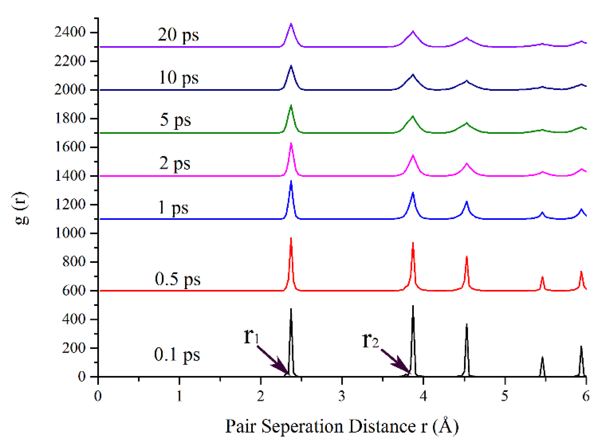
Figure 2 shows the RDF g(r) of the monocrystalline silicon target at different times during the 0.5 keV Si35 cluster implantation. It was found that silicon atoms only occupied several specific distances from the center atom, such as r1 of 2.35 Å and r2 of 3.84 Å. These two distances are the first neighbor distance and the second neighbor distance in silicon, respectively. Because Si35 cluster ions only knock on the target surface at 0.1 ps, the silicon target represents a perfect diamond lattice structure and has a long-range order. Elastic collisions were generated between cluster ions and target atoms, and collision cascades dramatically increased. Silicon atoms migrated from their initial lattice sites when the obtained kinetic energies exceeded their displacement threshold energies via an elastic collision. After that, the peaks of RDF decrease at every neighbor distance until 2 ps. It is suggested that many of the Frankel pairs, which are composed of vacancies and interstitial atoms, recombine in this stage. From 2 ps to 20 ps, the RDF curves almost never change and show that the damage has formed a stable structure. This result is in agreement with ~ 2 ps in a different material [23]. Interstitial atoms only possess local rearrangements, without much change in their positions from 2 ps.
Figure 3 shows the RDF comparison during the implantation of Si35 cluster ions with different kinetic energies. The peak value of the RDF at each neighbor distance decreases with the increase of the total kinetic energy of the cluster ions. This suggests that an energetic cluster with a higher kinetic energy can induce more damage in the target.

3.2. Vacancy Generation and Migration during Si35 Cluster Implantation

On the basis of Section 3.1, it is demonstrated that the silicon target rapidly changes its internal lattice structure due to the implantation of energetic cluster ions within 2 ps. As one form of change in the internal lattice structure, vacancies induce target damage. Therefore, we first measured vacancy generation and migration within 2 ps. In order to study vacancy generation and migration in the silicon target during Si35 cluster implantation, Wigner–Seitz cell analysis [24] was applied in this work. A Wigner–Seitz (W–S) cell is a primitive cell enclosed with perpendicular planes at the midpoint of the lines between a center atom and the nearest atoms.
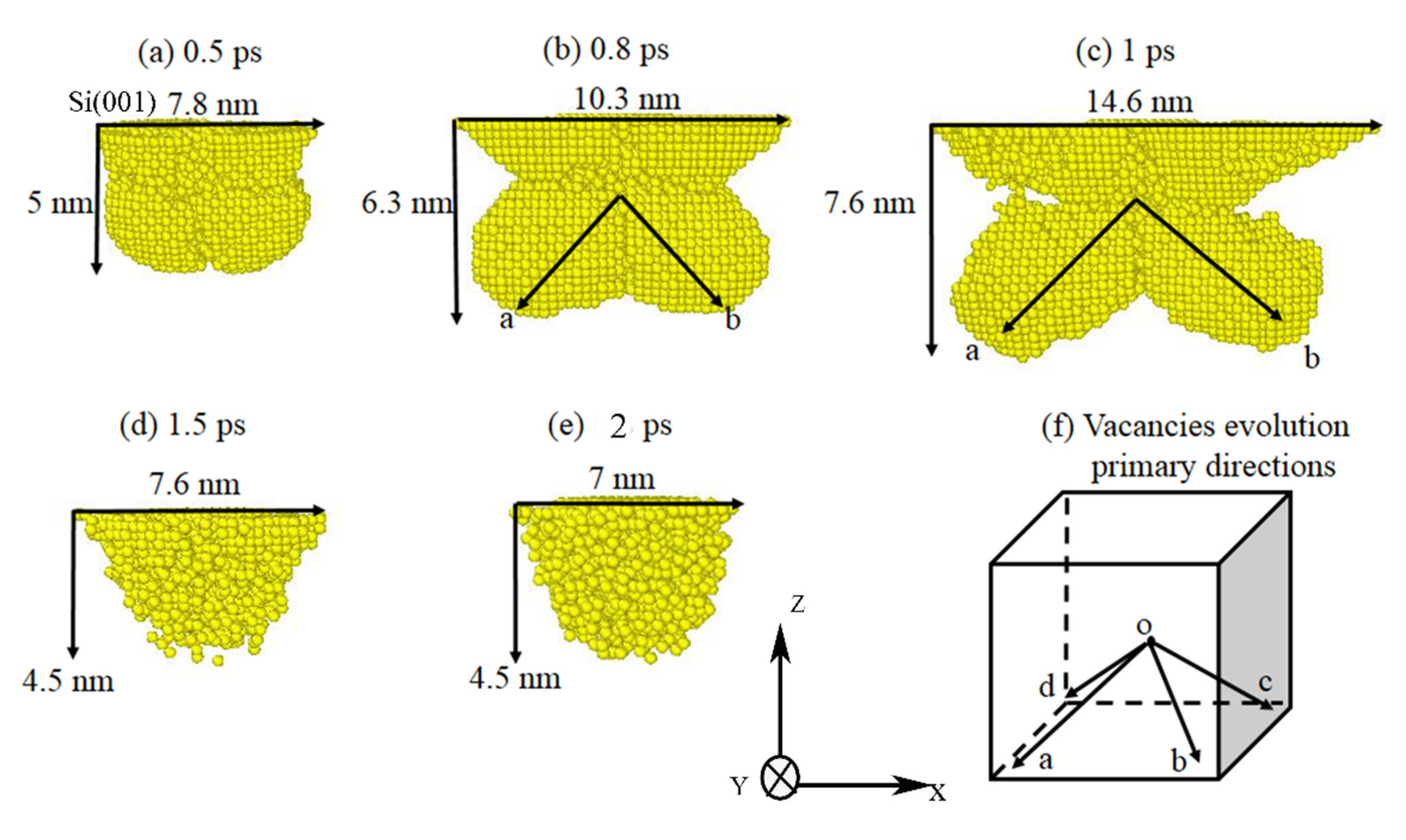
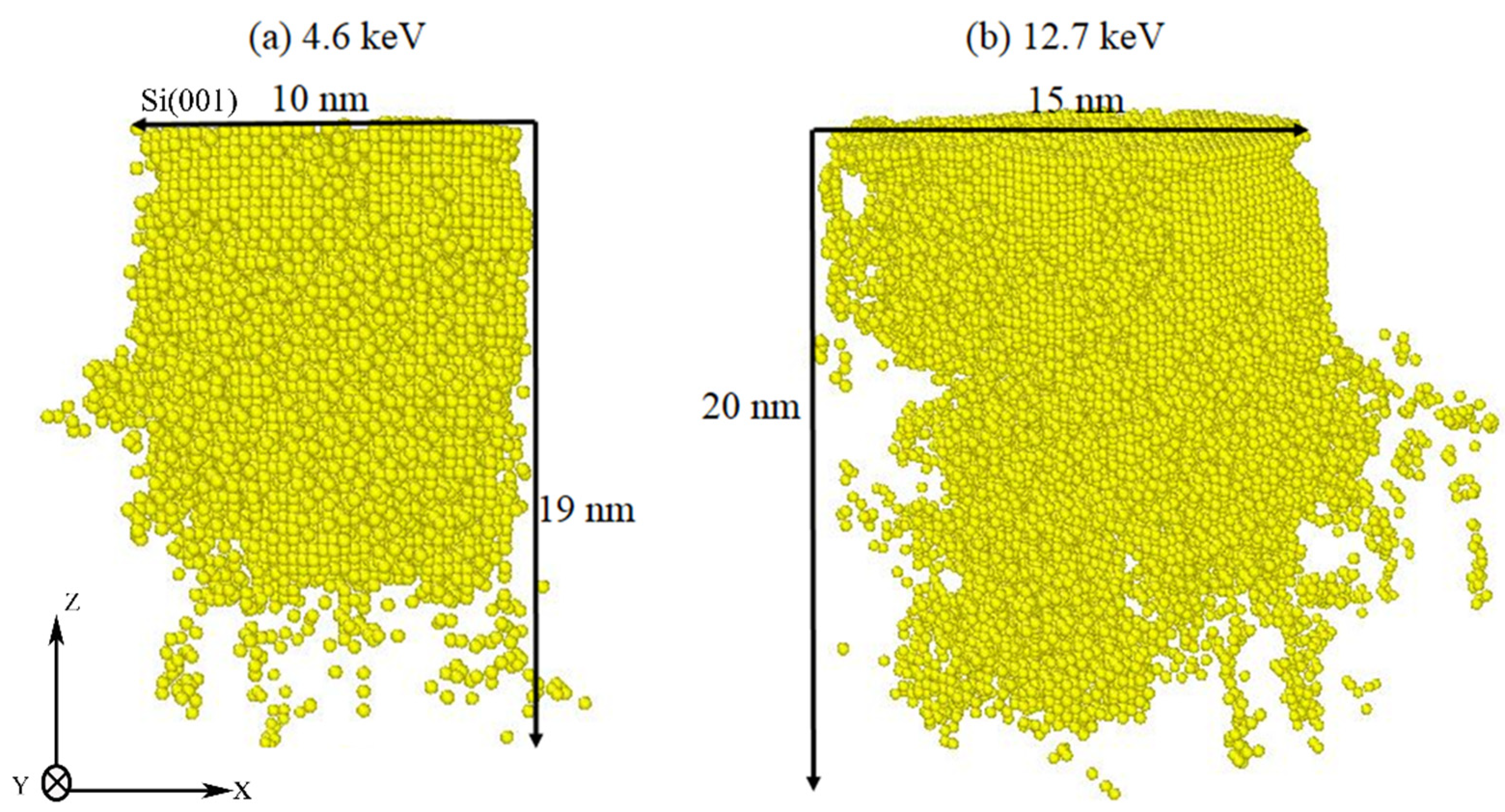
Figure 4 shows vacancies’ evolution in the silicon target during 0.5 keV Si35 cluster implantation. At the beginning of vacancies generation, vacancies are generated with a hemispherical morphology along the negative Z axis direction, as shown in Figure 4a. However, from 0.8 ps, vacancies are generated in four primary directions, which are the four body diagonal directions from a cubic center shown in Figure 4f, and form four hemispherical structures in the silicon target. Then, due to the continuous increase in collision cascades, vacancies are generated to the maximum in the four primary directions at 1 ps. After that, the recombination of vacancies and interstitial atoms occurs faster than the generation of vacancies. At the end, the vacancies in the silicon almost never changed, as shown in Figure 4d,e. These processes suggest that vacancies are generated in primary directions rather than random directions. In order to compare these results, we also measured vacancies’ evolution in the silicon target during 4.6 keV and 12.7 keV Si35 cluster implantation, as shown in Figure 5. It was found that vacancies were never generated in the four primary directions in the two cases: the incident direction of the cluster is the primary direction of vacancy evolution.
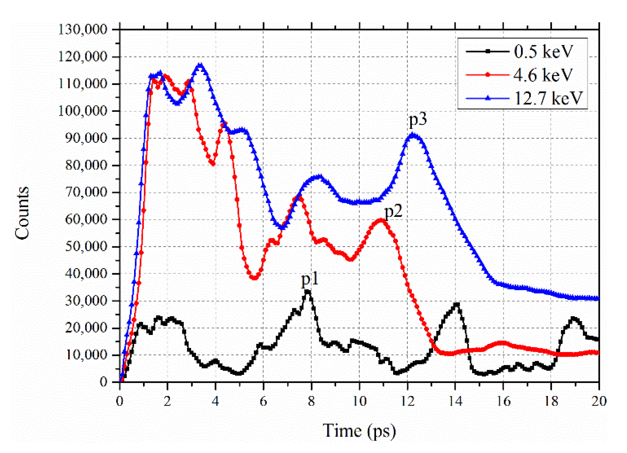
The time dependencies of vacancy generation and migration in the silicon target during three kinds of cluster implantations were also analyzed (Figure 6). In the first picosecond, vacancies rapidly increased to their maximal peak, and the cluster ions with higher incident kinetic energies induced more vacancies. After 2 ps, vacancies began to decrease due to the rapid recombination of vacancies and interstitial atoms. This decreasing trend did not reach the equilibrium state in the silicon target, but several increased vacancy peaks were generated in the silicon target, such as p1, p2, and p3 peaks. This is because target boundaries can emit interstitial atoms to a target and generate vacancies when implantation-induced vacancies reach the boundaries. This explanation was verified by a previous study [25]. It is suggested that boundaries have a loading–unloading effect, where interstitial atoms load into the boundary, which then acts as a source, emitting interstitial atoms to the target and inducing the formation of vacancies again.

3.3. Identify Diamond Structure Analysis

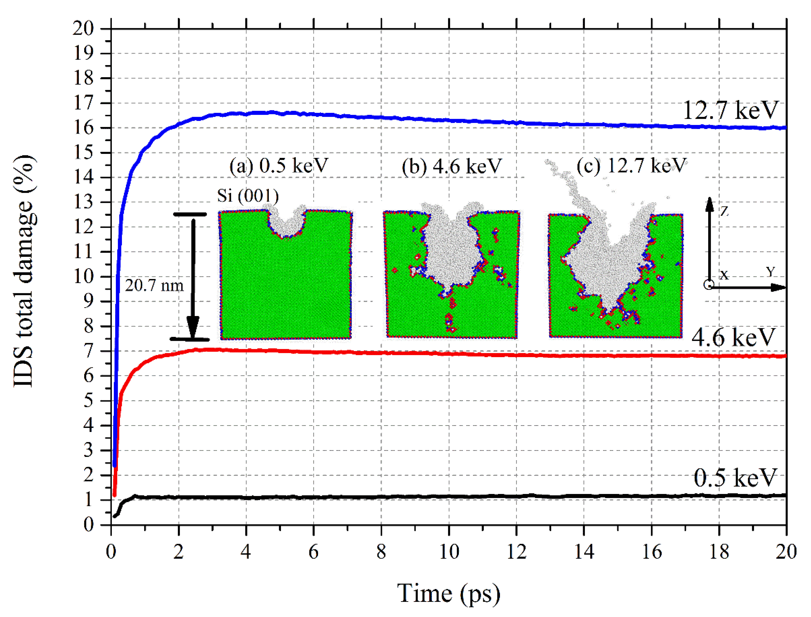
The cluster ions implantation-induced generation and migration of vacancies resulted in damages to the silicon target. In order to investigate the degree of damage during cluster implantation, we used identify diamond structure (IDS) analysis [26] to distinguish the diamond lattice structure and amorphous structure. Figure 7 shows the total IDS damage in the target during three kinds of cluster implantations. It was found that cluster ions with higher incident kinetic energies can induce more IDS total damage. The damages rapidly reach maximal peaks within the first two picoseconds and never change after two picoseconds. However, the amorphous morphologies of the three cases are different from each other. Figure 7a shows a hemispheric amorphous morphology, while Figure 7b,c show approximate conical amorphous morphologies. When comparing the three cases, we found that cluster ions with a higher incident kinetic energy induce a deeper amorphous structure.

4. Conclusions

In summary, we have described vacancy generation and migration near the monocrystalline silicon surface during energetic Si35 cluster implantation by using MD simulations. To illustrate vacancy generation, migration, and implantation-induced damage, we have used RDF, W-S cell, and IDS analytical methods in this work. Our results have demonstrated that, for the three implantation conditions, a lot of vacancies are rapidly generated and migrate in primary directions and form amorphous structures within the first two picoseconds. Clusters with a higher incident kinetic energy can induce the generation and migration of more vacancies and a deeper amorphous structure. Moreover, boundaries have a loading–unloading effect, where interstitial atoms load into the boundary, which then acts as a source, emitting interstitial atoms to the target and inducing the generation of vacancies again. These results can be used to better understand the doping of silicon via ion implantation.

Author Contributions

Conceptualization, G.L. and H.Z.; methodology, G.L., Y.W., and X.Y.; software, S.Z., M.X., and S.K.; formal analysis J.R., N.Z., and S.Y.; writing—original draft preparation, G.L. and X.Y.; writing—review and editing X.Y. and H.Z.; funding acquisition, G.E.R. and X.L. All authors have read and agreed to the published version of the manuscript.

Funding

This work was supported by National Natural Science Foundation of China (Grant No. 11875084) and the National Magnetic Confinement Fusion Program (Grant No. 2013GB109004).

Conflicts of Interest

The authors declare no conflict of interest.

References

  1. Current, M.I. Ion implantation of advanced silicon devices : Past, present and future. Mater. Sci. Semicond. Process. 2017, 62, 13–22. [Google Scholar] [CrossRef]
  2. Schultz, P.J.; Jagadish, C.; Ridgway, M.C.; Elliman, R.G.; Williams, J.S. Crystalline-to-amorphous transition for Si-ion irradiation of Si(100). Phys. Rev. Lett. 1991, 44, 9118–9121. [Google Scholar] [CrossRef] [PubMed]
  3. Pelaz, L.; Marqús, L.A.; Barbolla, J. Ion-beam-induced amorphization and recrystallization in silicon. J. Appl. Phys. 2004, 96, 5947–5976. [Google Scholar] [CrossRef]
  4. Wallace, J.B.; Bayu Aji, L.B.; Shao, L.; Kucheyev, S.O. Deterministic Role of Collision Cascade Density in Radiation Defect Dynamics in Si. Phys. Rev. Lett. 2018, 120, 216101. [Google Scholar] [CrossRef] [PubMed] [Green Version]
  5. Kempton, W.; Tomic, J. Vehicle-to-grid power fundamentals: Calculating capacity and net revenue. J. Power Sources 2005, 144, 268–279. [Google Scholar] [CrossRef]
  6. Baktash, A.; Sasani, A.; Alavizargar, A.; Mirabbaszadeh, K. First principle study of Nb defects in anatase (101) TiO2 surface. Mat. Sci. Semicon. Proc. 2016, 45, 45–50. [Google Scholar] [CrossRef]
  7. Nordlund, K.; Samela, J. Atomic flows, coronas and cratering in Au, Si and SiO2. Nucl. Instrum. Methods Phys. Res. Sect. B Beam Interact. Mater. Atoms 2009, 267, 1420–1423. [Google Scholar] [CrossRef]
  8. Lively, M.; Holybee, B.; Toriyama, M.; Allain, J. Massive-scale molecular dynamics of ion-irradiated III–V compound semiconductors at the onset of nanopatterning. Nucl. Instruments Methods Phys. Res. Sect. B Beam Interact. Mater. Atoms 2017, 409, 282–287. [Google Scholar] [CrossRef]
  9. Osmani, O.; Alzaher, I.; Peters, T.; Ban d’Etat, B.; Cassimi, A.; Lebius, H.; Monnet, I.; Medvedev, N.; Rethfeld, B.; Schleberger, M. Damage in crystalline silicon by swift heavy ion irradiation. Nucl. Instruments Methods Phys. Res. Sect. B Beam Interact. Mater. Atoms 2012, 282, 43–47. [Google Scholar] [CrossRef]
  10. Wallace, J.B.; Bayu Aji, L.B.; Shao, L.; Kucheyev, S.O. Fractal analysis of collision cascades in pulsed-ion-beam-irradiated solids. Sci. Rep. 2017, 7, 17574. [Google Scholar] [CrossRef] [Green Version]
  11. Aoki, T.; Seki, T.; Matsuo, J. Molecular dynamics simulation study of damage formation and sputtering with huge fluorine cluster impact on silicon. Nucl. Instruments Methods Phys. Res. Sect. B Beam Interact. Mater. Atoms 2013, 303, 170–173. [Google Scholar] [CrossRef]
  12. Aoki, T. Molecular dynamics simulations of cluster impacts on solid targets: Implantation, surface modification, and sputtering. J. Comput. Electron. 2014, 13, 108–121. [Google Scholar] [CrossRef] [Green Version]
  13. Azarov, A.Y.; Titov, A.I.; Karaseov, P.A.; Hallén, A. Effect of collision cascade density on radiation damage in SiC. Nucl. Instrum. Methods Phys. Res. Sect. B Beam Interact. Mater. Atoms 2009, 267, 1247–1250. [Google Scholar] [CrossRef]
  14. Yu, X.; Shen, J.; Zhong, H.; Zhang, J.; Yan, S.; Zhang, G.; Zhang, X.; Le, X. Thermo-hydrodynamic process simulation of craters formation and evolution on metal surfaces caused by intense pulsed ion beams. Vacuum 2015, 120, 116–120. [Google Scholar] [CrossRef]
  15. Shen, J.; Yu, X.; Zhang, J.; Zhong, H.; Cui, X.; Liang, G.; Yu, X.; Huang, W.; Shahid, I.; Zhang, X.; et al. Anisotropy effect of crater formation on single crystal silicon surface under intense pulsed ion beam irradiation. Nucl. Instrum. Methods Phys. Res. Sect. B Beam Interact. Mater. Atoms 2018, 421, 7–12. [Google Scholar] [CrossRef]
  16. Xiao, Y.J.; Fang, F.Z.; Xu, Z.W.; Hu, X.T. Annealing recovery of nanoscale silicon surface damage caused by Ga focused ion beam. Appl. Surf. Sci. 2015, 343, 56–69. [Google Scholar] [CrossRef]
  17. Plimpton, S. Fast parallel algorithms for short-range molecular dynamics. J. Comput. Phys. 1995, 117, 1–19. [Google Scholar] [CrossRef] [Green Version]
  18. Ziegler, J.; Biersack, J.; Littmark, U. The Stopping and Range of Ions in Solids; Pergamon Press: New York, NY, USA, 1985. [Google Scholar] [CrossRef] [Green Version]
  19. Tersoff, J. Modeling solid-state chemistry: Interatomic potentials for multicomponent systems. Phys. Rev. B 1989, 39, 5566–5568. [Google Scholar] [CrossRef]
  20. Stukowski, A. Visualization and analysis of atomistic simulation data with OVITO-the Open Visualization Tool. Model. Simul. Mater. Sci. Eng. 2010, 18, 015012. [Google Scholar] [CrossRef]
  21. Liu, S.; Li, H.; He, Y.; Li, X.; Li, Y.; Wang, X. Pathway into the silicon nucleation on silicene substrate at nanoscale. Mater. Des. 2015, 85, 60–66. [Google Scholar] [CrossRef]
  22. Fang, K.C.; Weng, C.I.; Ju, S.P. An investigation into the structural features and thermal conductivity of silicon nanoparticles using molecular dynamics simulations. Nanotechnology 2006, 17, 3909–3914. [Google Scholar] [CrossRef]
  23. Peng, Q.; Meng, F.; Yang, Y.; Lu, C.; Deng, H.; Wang, L.; De, S.; Gao, F. Shockwave generates <100 > dislocation loops in bcc iron. Nat. Commun. 2018, 9. [Google Scholar] [CrossRef]
  24. Wigner, E.; Seitz, F. On the constitution of Metallic Sodium. Phys. Rev. 1933, 68, 804–810. [Google Scholar] [CrossRef]
  25. Bai, X.M.; Voter, A.F.; Hoagland, R.G.; Nastasi, M.; Uberuaga, B.P. Efficient annealing of radiation damage near grain boundaries via interstitial emission. Science 2010, 327, 1631–1634. [Google Scholar] [CrossRef] [PubMed]
  26. Maras, E.; Trushin, O.; Stukowski, A.; Ala-Nissila, T.; Jónsson, H. Global transition path search for dislocation formation in Ge on Si(001). Comput. Phys. Commun. 2016, 205, 13–21. [Google Scholar] [CrossRef] [Green Version]
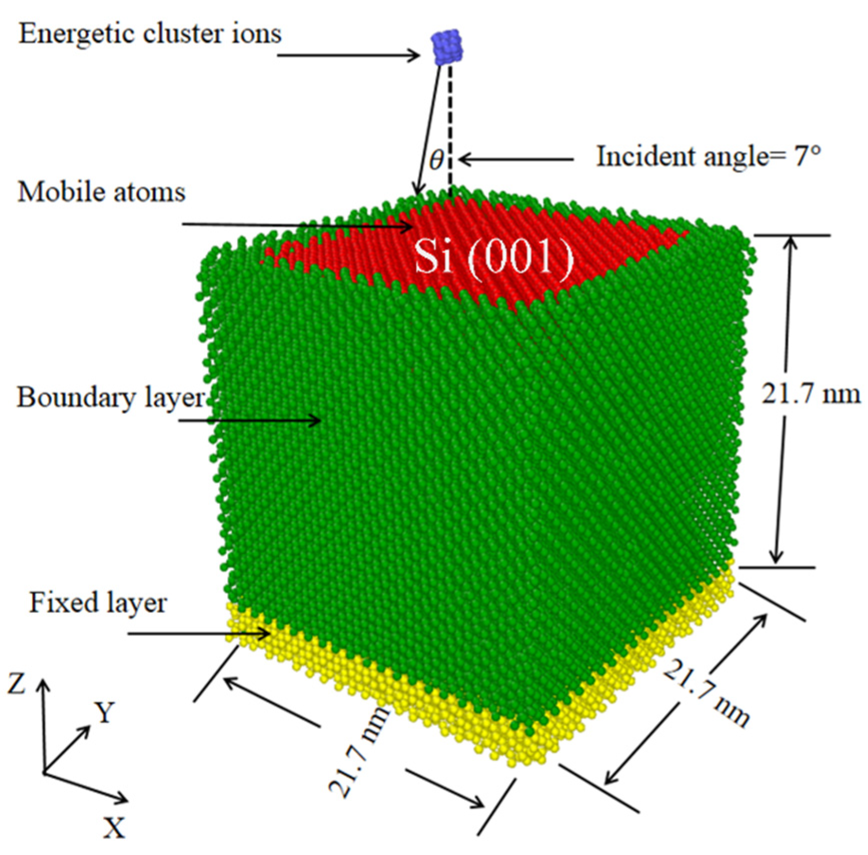
Figure 1. The three-dimensional molecular dynamics (MD) model for energetic cluster ion implantation into a monocrystalline silicon target.
Coatings 10 00146 g001
Figure 2. Radial distribution function of the silicon target during 0.5 keV Si35 cluster implantation. r1 is the first neighbor distance, and r2 is the second neighbor distance.
Coatings 10 00146 g002
Figure 3. Radial distribution function of the silicon target during 0.5 keV, 4.6 keV, and 12.7 keV Si35 cluster implantation.
Coatings 10 00146 g003
Figure 4. Cross-sectional views of the primary directions of vacancies’ evolution in the silicon target during 0.5 keV Si35 cluster implantation from 0.5 ps to 2 ps. The yellow dots represent vacancies. The top surface is the Si (001) plane. The directions of (ad) in (f) are the primary directions of vacancies’ evolution.
Coatings 10 00146 g004
Figure 5. Cross-sectional views of vacancies’ evolution in the silicon target during (a) 4.6 keV and (b) 12.7 keV Si35 cluster implantation at 0.5 ps. The yellow dots represent vacancies. The top surface is the Si (001) plane.
Coatings 10 00146 g005
Figure 6. Time dependencies of vacancies’ evolution in the silicon target during 0.5 keV, 4.6 keV, and 12.7 keV Si35 cluster implantation. p1, p2, and p3 represent different vacancy peaks.
Coatings 10 00146 g006
Figure 7. Identify diamond structure (IDS) total damage to the silicon target as a function of time during (a) 0.5 keV, (b) 4.6 keV, and (c) 12.7 keV Si35 cluster implantation. The insets represent the cross-sectional view of IDS damage in the target at 10 ps. The green dots represent silicon atoms, the red dots represent the first neighbor silicon atoms, the blue dots represent the second neighbor silicon atoms, and the gray dots represent amorphous atoms.
Coatings 10 00146 g007