Article

Electrical Characteristics and Stability Improvement of Top-Gate In-Ga-Zn-O Thin-Film Transistors with Al2O3/TEOS Oxide Gate Dielectrics

1
Department of Electro-Optical Engineering, Minghsin University of Science and Technology, Hsinchu 30401, Taiwan
2
Department of Materials Science and Engineering, National Chiao Tung University, Hsinchu 30010, Taiwan
3
Department of Electronic Engineering, National United University, Miaoli 360, Taiwan
*
Author to whom correspondence should be addressed.
Coatings 2020, 10(12), 1146; https://doi.org/10.3390/coatings10121146
Submission received: 28 August 2020 / Revised: 30 October 2020 / Accepted: 20 November 2020 / Published: 24 November 2020
(This article belongs to the Special Issue Advances in Thin Film Transistors: Properties and Applications)

Abstract

:
In this work, two stacked gate dielectrics of Al2O3/tetraethyl-orthosilicate (TEOS) oxide were deposited by using the equivalent capacitance with 100-nm thick TEOS oxide on the patterned InGaZnO layers to evaluate the electrical characteristics and stability improvement of amorphous indium gallium zinc oxide (a-IGZO) thin-film transistors (TFTs) devices, including positive bias stress (PBS) and negative bias stress (NBS) tests. Three different kinds of gate dielectrics (Al2O3, TEOS, Al2O3/TEOS) were used to fabricate four types of devices, differing by the gate dielectric, as well as its thickness. As the Al2O3 thickness of Al2O3/TEOS oxide dielectric stacks increased, both the on-current and off-current decreased, and the transfer curves shifted to larger voltages. The lowest ∆Vth of 0.68 V and ∆S.S. of −0.03 V/decade from hysteresis characteristics indicate that the increase of interface traps and charge trapping between the IGZO channel and gate dielectrics is effectively inhibited by using two stacked dielectrics with 10-nm thick Al2O3 and 96-nm thick TEOS oxide. The lowest ∆Vth and ∆S.S. values of a-IGZO TFTs with 10-nm thick Al2O3 and 96-nm thick TEOS oxide gate dielectrics according to the PBS and NBS tests were shown to have the best electrical stability in comparison to those with the Al2O3 or TEOS oxide single-layer dielectrics.

1. Introduction

Amorphous oxide semiconductors (AOSs) are promising for channel materials of thin-film transistors [1,2] (TFTs) and are feasible for driving TFTs in organic light-emitting diode displays due to their large carrier mobility (>10 cm2 V−1 s−1) and low process temperatures. The conventional bottom-gate structure has been widely studied for amorphous indium gallium zinc oxide (a-IGZO) TFTs [3,4]. However, this structure is unsuitable for integration onto the glass of peripheral circuits for the system and for the realization of high-resolution, high-quality active-matrix organic light-emitting diode (AMOLED) displays due to the high parasitic capacitance and poor scalability. Therefore, the development of self-aligned top-gate oxide TFTs with good performance and high stability is necessary for AMOLED display applications [5,6]. A constant positive VG_STRESS is known to induce a rigid, positive shift in the transfer characteristics of a-IGZO TFTs [7,8,9,10]. The voltage shift is attributed to the trapping of carriers (electrons) at the active-layer/gate-insulator interface and/or in the gate-insulator without the generation of new trap sites or defects. This trapped charge screens the applied electric field, resulting in the reduction of the effective applied VG and in the positive threshold voltage shift of Vth. Similarly, a constant negative gate bias-stress (VG_STRESS) is known to induce hole trapping and/or the generation of doubly ionized oxygen-vacancies (VO2+), which donate two electrons to the semiconductor conduction band. Either one or both of these events lead to the negative threshold voltage shift of Vth [7,11,12]. However, these mechanisms are valid for a-IGZO TFTs without source and drain-offsets, such as the conventional bottom-gate inverted-staggered structures. Mativenga et al. [13] showed the reason why the gate dielectric SiO2 layer is applied to the various gate bias-stresses (VG_STRESS) of the top-gate structure and why the bias voltage (bias stress) is used in detail. The migration of positive charges towards the offsets lowers the local resistance of the offsets, resulting in an abnormal negative Vth under positive VG_STRESS. The negative threshold voltage shift (∆Vth) suggests the induction of excess electrons in the channel, which can only be explained by the bias-induced generation of donor states, such as H+ or ionized oxygen vacancies. Negative VG_STRESS induces the migration of positive charges from the offsets and towards the region of the channel that is located underneath the gate metal. Consequently, the reduction in on-current under negative VG_STRESS is due to the increase in resistance of the offsets when positive charges migrate away from the offsets. However, oxide-based TFTs typically require large operating voltages (VG) to achieve high mobility and high on-off current ratios. In addition to using high-mobility semiconductors, operating voltages can be reduced by developing gate dielectric materials capable of large capacitance densities with low leakage currents that have good compatibility for the growth of the semiconductor channel, leading to low trap densities at the semiconductor-gate dielectric interface [14]. With a high dielectric constant (high-k) of 9 and a large band gap of 8 eV, Al2O3 is a good candidate to produce gate dielectrics with low leakage and high capacitance density. However, the electrical stability of the a-IGZO TFT with a high-k gate dielectric layer is one of the critical issues, especially under the positive bias stress (PBS) [15,16]. Chang et al. reported the stability of low-temperature a-IGZO thin-film transistors (TFTs), which was evaluated using gate stress voltages of 10 V and −10 V (3.3 MV/cm) for PBS and negative bias stress (NBS), respectively, at room temperature. The initial positive ∆Vth was explained by the electron trapping in Al2O3, which was also evident in an a-IGZO TFT with a high-temperature atomic layer deposition (ALD) Al2O3 dielectric deposited at 250 °C [17]. With the same temperature used for depositing the Al2O3 gate dielectric as that in this paper, the electron trapping in traps located at the interface and bulk Al2O3 layers was responsible for the initial positive ∆Vth.
In this work, top-gate a-IGZO TFT devices with two stacked Al2O3/tetraethyl-orthosilicate (TEOS) gate dielectrics were fabricated on silicon wafers, then electrical characteristics and instability, including PBS and NBS tests were measured. Moreover, two stacked dielectrics of Al2O3/ TEOS oxide were deposited by using the equivalent capacitance with 100-nm thick TEOS oxide on the patterned IGZO layers to evaluate the electrical characteristics and stability improvement of the a-IGZO TFT devices. By using two stacked dielectrics with 10-nm thick Al2O3 and 96-nm thick TEOS oxide can effectively inhibit the increase of interface traps and charge trapping between the IGZO channel and gate dielectrics. In addition, in order to compare the effect of the thickness of Al2O3, the deposit of a 20-nm thick Al2O3 gate dielectric on the patterned IGZO layers was prepared.

2. Experimental Methods

Figure 1a shows the cross-sectional diagram of the top-gate a-IGZO TFT structure used in this study. The devices were fabricated on a 101.6 mm in diameter silicon wafer capped with 500-nm thick thermally grown silicon dioxide (SiO2) as a buffer layer. First, a-IGZO films with a thickness of 40 nm were deposited through radio frequency (RF) magnetron sputtering by using an IGZO target with an atomic ratio of In:Ga:Zn:O = 1:1:1:4 at room temperature under a fixed deposited power of 100 W. The system based and working pressures were 3 × 10⁻⁶ Torr and 5 m Torr, respectively. During sputter, the flow rates of Ar/O2 were fixed at 50/1 standard cubic centimeters per minute (sccm). The a-IGZO channel layer was patterned to define the channel width by photolithography. Subsequently, dry etching using inductively coupled plasma (ICP) of a Nasca-20 Plus dry etching system with a mixed gas of Cl2/Ar = 45/9 sccm was performed under a top electrode’s power of 300 W and a bottom electrode’s power of 30 W. Then, two stacked dielectrics of Al2O3/TEOS oxide were deposited by using the equivalent capacitance with 100-nm thick TEOS oxide on the patterned IGZO layers. First, Oxford plasma-enhanced chemical vapor deposition (PECVD) system was applied to deposit a predetermined TEOS oxide thickness as the first layer of gate dielectrics at 350 °C under a fixed deposited power of 40 W. The system working pressure was 700 m Torr by using a mixed gas of Ar-TEOS/O2 = 50/300 sccm as the precursors. Subsequently, Ultratech Fiji G2 atomic layer deposition (ALD) system was applied to deposit a predetermined Al2O3 thickness as the second layer of gate dielectrics at 250 °C at a deposition rate of approximately 10 nm/1 hr by using Al(CH3)3 (trimethylaluminum, TMA) and H2O as sources for Al and O, respectively. In order to compare the effect of the thickness of Al2O3, the deposit of a 20-nm thick Al2O3 gate dielectric on the patterned IGZO layers was prepared. A 50-nm thick molybdenum (Mo) gate metal was deposited using RF magnetron sputtering at room temperature under a fixed deposited power of 100 W with an Ar gas flow of 20 sccm. The system based and working pressures were 2 × 10⁻⁶ Torr and 3 m Torr, respectively. The Mo gate metal was patterned to define the channel length by photolithography. Subsequently, dry etching of the gate metal was performed by using ICP with the same etching condition of the a-IGZO channel layer, followed by gate dielectrics etching with a mixed gas of CF4 (tetrafluoromethane)/O2 = 100/5 scan was performed under a top electrode’s power of 250 W and a bottom electrode’s power of 20 W. After gate etching, argon plasma treatment was performed by using the ICP system to activate the exposed surfaces of the a-IGZO channel layer under a top electrode’s power of 300 W and working pressure of 50 mTorr with an Ar gas flow of 150 sccm. A 100-nm thick SiO2 passivation was deposited using the PECVD system at 300 °C under a fixed deposited power of 20 W. The system working pressure was 1 Torr by using a mixed gas of SiH4/N2O/N2 = 8.5/710/161.5 sccm as the precursors. Afterwards, a lithographic step was performed to define the contact area; subsequently, dry etching was performed for SiO2 by using ICP with the same etching condition of the gate dielectrics etching. Finally, a 100-nm thick Mo source-drain metal using RF magnetron sputtering at room temperature was then formed by a lift-off process in contact with the exposed area of a-IGZO channels. After complete deposition, all the IGZO TFTs samples used in this study were annealed at 300 °C at a working pressure of 5 m Torr for 1 h in an N2 ambient atmosphere of 40 sccm to form an ohmic contact before electrical measurement. Process charts for each step of top-gate a-IGZO TFTs used in this study are summarized in Figure 1b.
IDSVGS transfer characteristics, which VGS varies from −15 V to +15 V in 0.3 V steps for VDS = 0.1 V, of all devices were executed using an Agilent 4156A precision semiconductor parameter analyzer, and the measurement temperature was maintained at 25 °C.
Devices with a channel width W of 100 µm and channel length L of 5 µm were selected for this experiment. The source and drain-offsets were designed at 1 µm and shown in Figure 1a. The field effect mobility (µFE) was calculated using
μ F E = L × G m m a x W × C o x × V D S
where Cox is the capacitance per unit area of the TEOS oxide, the transconductance (GM) = IDS/ VGS, and VDS = 0.1 V. The subthreshold swing (S.S.) was taken as the value of (dlog (IDS)/dVGS)−1 when the IDS was in the range from 10−10 A to 10−9 A.

3. Results and Discussions

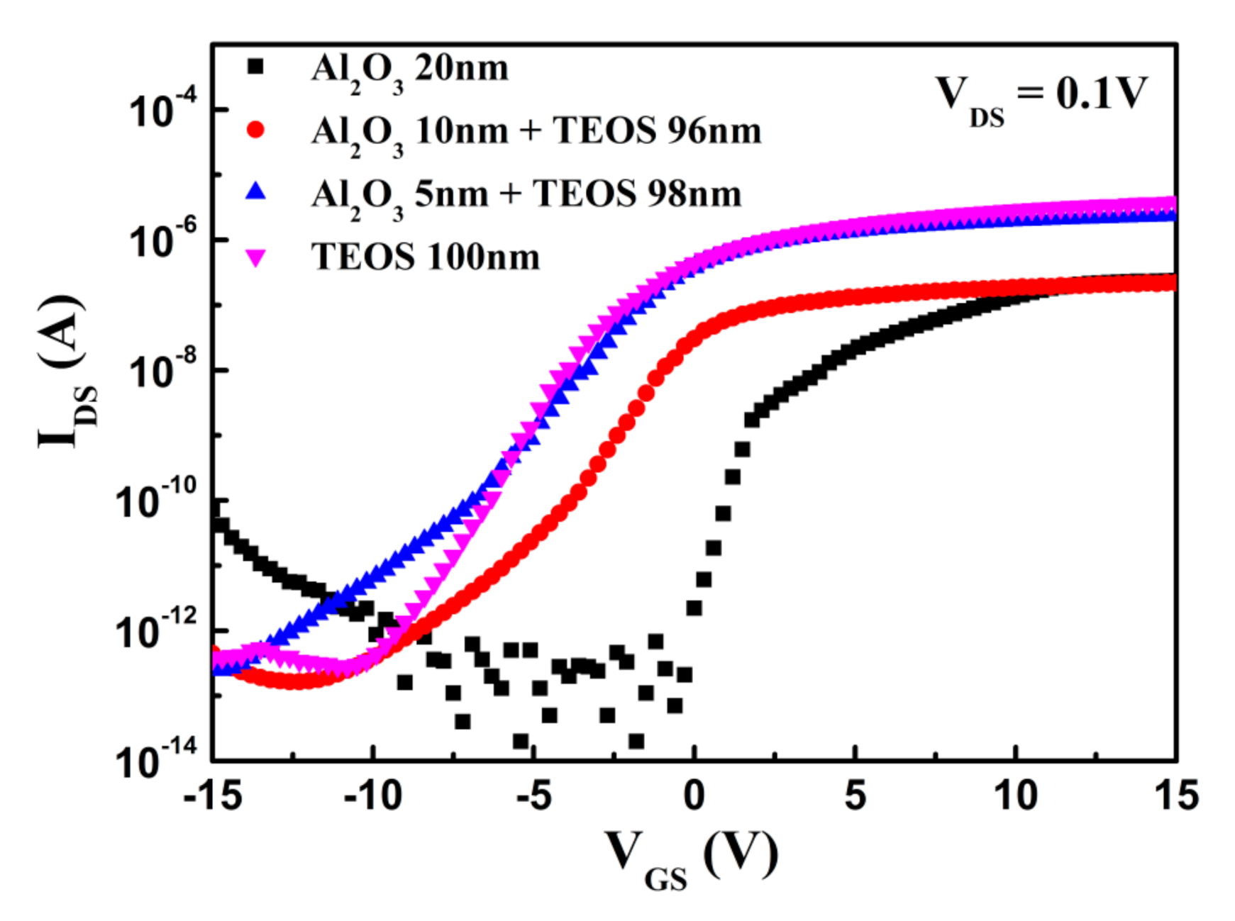
3.1. Electrical Characteristics of IGZO TFTs with Al2O3, Al2O3/TEOS Oxide, and TEOS Oxide Gate Dielectrics

Figure 2 shows the representative IDS-VGS transfer characteristics and extracted electrical parameters of a-IGZO TFTs at VDS = 0.1 V and W/L = 100/5 µm with Al2O3 (20 nm), Al2O3 (10 nm)/TEOS oxide (96 nm), Al2O3 (5 nm)/TEOS oxide (98 nm) and TEOS oxide (100 nm) gate dielectrics, respectively. The threshold voltage (Vth) is defined as the gate voltage (VGS) when the drain current (IDS) is a constant (10−9 × (W/L) A). The measurements were made with more than three samples in each device. The measured gate capacitance per unit area (Cox) of a 100 nm-TEOS oxide was 4.98 × 10⁻⁸ F/cm2. Table 1 shows the average values and standard variations of the extracted electrical parameters of a-IGZO TFTs with the investigated gate dielectric conditions, respectively. It is clearly confirmed in Figure 2 that the transfer curves shift positively with increasing Al2O3 gate dielectric thickness as a result of the low on-current (Ion) within the channel of a-IGZO TFTs with a thicker Al2O3 gate dielectric. Park et al. [18] reported that the presence of ALD-based Al2O3 increased the turn-on voltage and slightly and adversely decreased the mobility of bottom-gate a-IGZO TFTs with Al2O3/SiO2 double-layered dielectrics. From the summary in Table 1, the TEOS oxide dielectric possessed the largest on/off ratio of > 107, a S.S. slope of 1.08 V/decade, a Vth of −4.8 V and a μFE of 4.01 cm2 V−1 s−1. As the Al2O3 thickness of Al2O3/TEOS oxide dielectric stack increases, both the on-current and off-current decrease, and the transfer curves shift further to larger voltages. However, the S.S. values of top-gate a-IGZO TFTs with two stacked Al2O3/TEOS oxide gate dielectrics are larger than the values of the Al2O3 or TEOS oxide single-layer dielectric. The results indicate that two stacked Al2O3/TEOS oxide gate dielectrics have more interfacial states than the single-layer dielectric, whether Al2O3 or TEOS oxide. For the comparison of the effect of Al2O3 thickness, the 20-nm thick Al2O3 gate dielectric revealed an on/off ratio of around 107, a S.S. slope of 0.49 V/decade, a Vth of 1.6 V, and a μFE of 0.35 cm2 V−1 s−1. The results obviously indicate that the electrical characteristics of a-IGZO TFTs had more positive Vth, less S.S., and μFE corresponding to the increasing Al2O3 thickness.

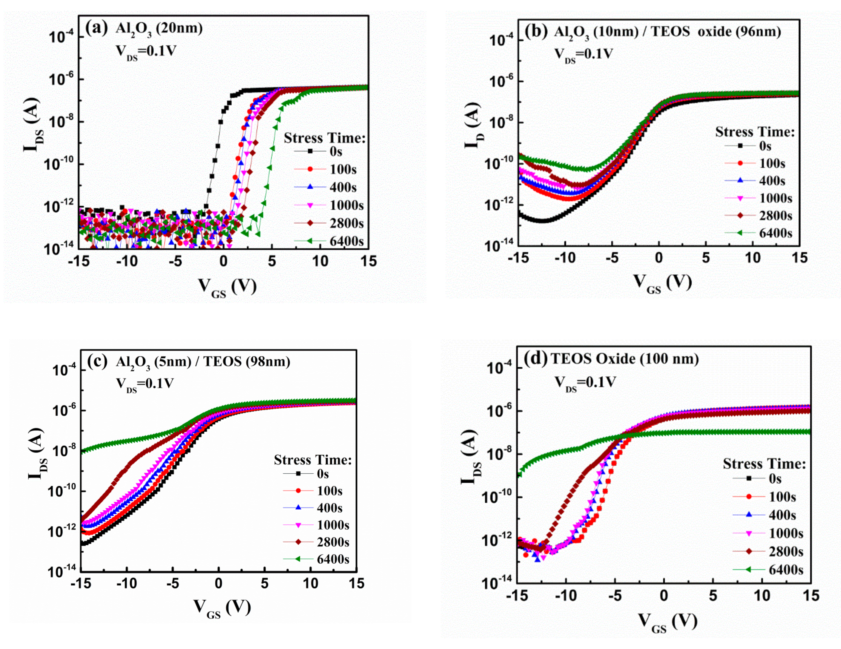
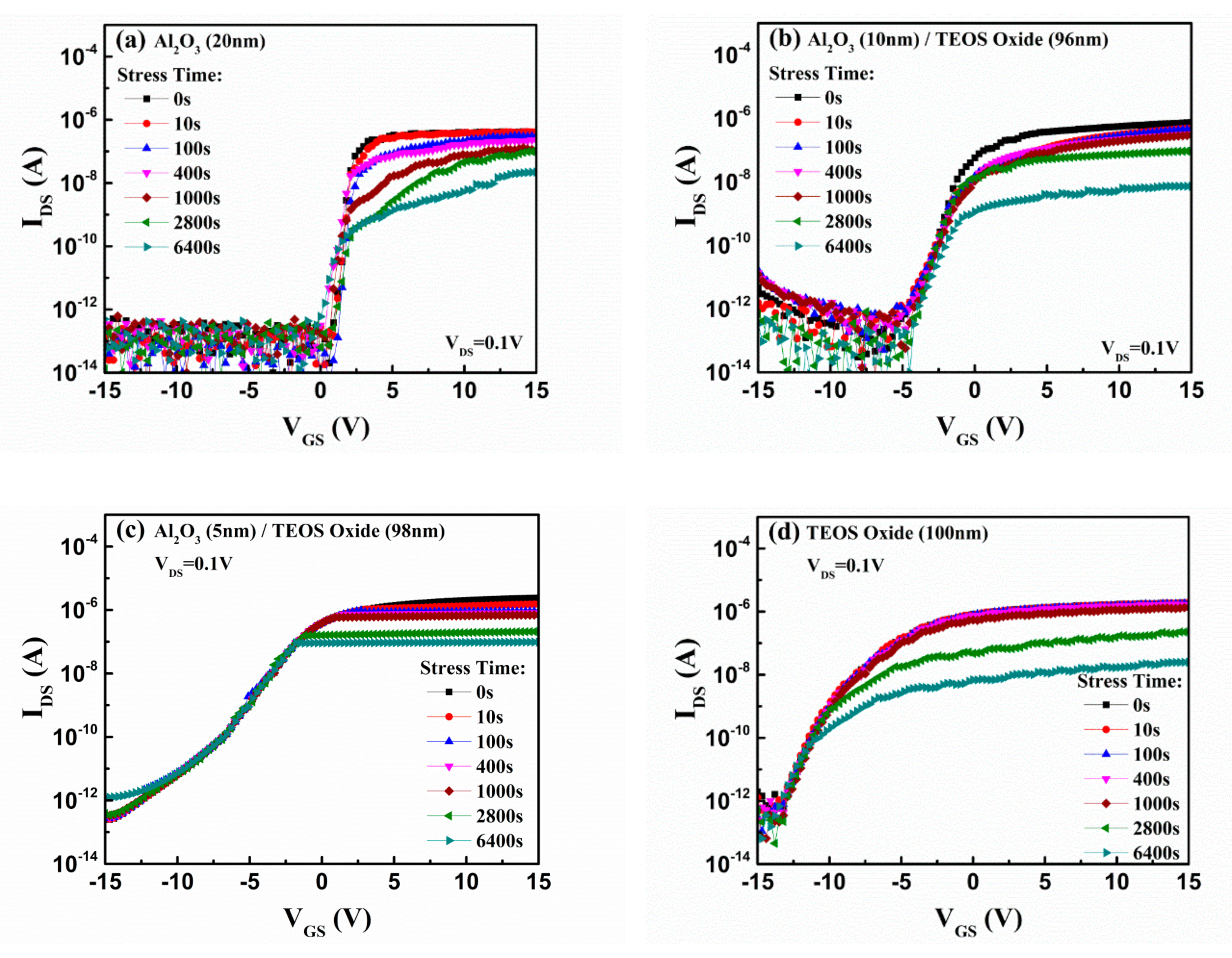
3.2. Electrical Instabilities of IGZO TFTs with Al2O3, Al2O3/TEOS Oxide, and TEOS Oxide Gate Dielectrics

Figure 3 show the IDS-VGS transfer characteristics of a-IGZO TFTs at VDS = 0.1 V and W/L = 100/5 µm with the four kinds of gate dielectrics as a function of stress over time under a positive bias-stress of 20 V [19]. The threshold voltage shift (∆Vth), the variety of the sub-threshold swing (∆S.S.), and the variance ratio of the on-current (∆Ion/Ion) of a-IGZO TFTs with four kinds of gate dielectrics after PBS stress for 6400 s are summarized in Table 2. After PBS, the transfer curves of the a-IGZO TFT with the Al2O3 (20 nm) dielectric were shifted positively, and the Vth was positively increased, as shown in Figure 3a. The increase of Vth has been frequently attributed to the charge trapping of accumulated electrons in the channel region at the gate dielectrics. Suresh et al. [20] demonstrated that the application of a gate bias stress to IGZO transparent TFTs with ALD AlOx and TiOx (ATO) gate dielectrics was found to induce a parallel threshold voltage shift without changing the field effect mobility or the subthreshold gate voltage swing. Table 2 shows the ∆Vth of a-IGZO TFTs with the two stacked Al2O3/TEOS oxide gate dielectrics are obviously lower than those with the Al2O3 or TEOS oxide single-layer dielectric. In addition, by increasing the Al2O3 thickness from 0 to 20 nm, the ∆S.S. decreases from 11.32 V/decade to 0.034 V/decade and ∆Ion/Ion decreases from −93% to −2.8% after a PBS stress of 6400 s, as shown in Figure 4b,c, respectively. The result of the variability of S.S. shows the increase of the interface traps between the channel and gate dielectrics is obviously inhibited by increasing the Al2O3 thickness in the application of top-gate a-IGZO TFTs devices. This is ascribed to the fact that the increase of the Al2O3 thickness of Al2O3/TEOS oxide dielectric stacks results in the decrease of excess electrons in the a-IGZO channel and the prohibition of electron traps in the gate dielectric stacks. Therefore, the on-current of a-IGZO TFTs is sustained by increasing the Al2O3 thickness of Al2O3/TEOS oxide dielectric stacks, as shown in Table 1. However, the PBS results of a-IGZO TFTs with the 20 nm Al2O3 gate dielectric show that the largest positive ∆Vth is +5.75 V. The positive ∆Vth is explained by the electron trapping in Al2O3, which was also evident in the a-IGZO TFT with a high-temperature ALD Al2O3 dielectric deposited at 250 °C [17]. Electron traps in gate dielectrics result in fewer electrons inside the IGZO channel; therefore, a more positive gate voltage will be applied to accumulate the necessary electrons for conductance in the channel. It is noticeable that the off-current of a-IGZO TFTs with a 20 nm Al2O3 gate dielectric is sustained at lower values of around 10−13 A after the PBS test for 6400 s. In addition, the PBS results of a-IGZO TFTs with the 100 nm TEOS oxide gate dielectric showed the largest negative ∆Vth of −8.8 V, suggesting the induction of excess electrons in the channel, which can only be explained by the bias-induced generation of donor states such as H+ or ionized oxygen vacancies [12]. However, the lowest ∆Vth of −0.42 V of a-IGZO TFTs with 10-nm thick Al2O3 and 96-nm thick TEOS oxide shows that the increase of interface traps and charge trapping between the IGZO channel and gate dielectrics is obviously inhibited by using two stacked dielectrics.
To investigate the effects of the Al2O3 and TEOS oxide gate dielectrics and their interface with the a-IGZO active layer, hysteresis sweeps of a-IGZO TFTs with four kinds of gate dielectrics were examined. Figure 4a shows the hysteresis characteristics of the a-IGZO TFT with the 20 nm Al2O3 gate dielectric as a function of the gate voltage (VGS) ranging from −15 V to +15 V. The largest threshold voltage shift (∆Vth = −3.04 V) and degradation of subthreshold swing (∆S.S. = +0.23 V/decade) from the hysteresis loop indicated that more electrons were trapped at or near the Al2O3/a-IGZO interface or within the a-IGZO channel layer. Fran et al. reported that the hysteresis voltage abnormally shifted towards the negative direction, and the negative Vth shift is due to the carrier creation in the IGZO film, which is mainly from the enhanced control and from using the high-k HfO2 as the gate insulator [15,21]. In addition, Figure 4b–d show the hysteresis characteristics of a-IGZO TFTs with the Al2O3 (10 nm)/TEOS oxide (96 nm), Al2O3 (5 nm)/TEOS oxide (98 nm), and TEOS oxide (100 nm) gate dielectrics, respectively. The lower threshold voltage shifts (∆Vth= 0.68 V, 0.84 V, and 0.99 V) and degradation of subthreshold swing (∆S.S. = −0.03, −0.18, and −0.02 V/decade) calculated from the respective hysteresis loops in Figure 4b–d indicated that few electrons were trapped at or near the TEOS oxide/a-IGZO interface or within the a-IGZO channel layer. The lowest ∆Vth of 0.68 V and ∆S.S. of −0.03 V/decade from the hysteresis loop in Figure 4b show that the increase of interface traps and charge trapping between the IGZO channel and gate dielectrics is effectively inhibited by using two stacked dielectrics with 10-nm thick Al2O3 and 96-nm thick TEOS oxide. Carlos et al. mentioned that the Si–OH absorbance band was not detected in a typical Fourier transform infrared spectroscopy (FTIRS) study of the deposited TEOS oxide [22]. In general, the effect of hydroxyl (OH) groups in polymeric dielectrics on the organic transistor’s hysteresis performance is a strongly proportional relationship [23]. Moreover, Jeon et al. showed that in order to utilize an Al2O3 high-k layer in IGZO TFTs, the interfacial SiO2 layer is crucial to lower both the interface state density and charge trapping by studying the conductance loss versus gate voltage and hysteresis sweep of the metal-oxide-semiconductor (MOS) capacitors with an Al2O3 single gate dielectric and Al2O3/SiO2 gate dielectrics [24]. The reasons why the lower ∆Vth of a-IGZO TFTS with two stacked Al2O3/TEOS oxide gate dielectrics after PBS tests can be explained.
Figure 5 show the transfer characteristics a-IGZO TFTs with the four kinds of gate dielectrics as a function of stress over time under a negative bias-stress of 20 V. ∆Vth, ∆S.S., and ∆Ion/Ion of a-IGZO TFTs with the four kinds of gate dielectrics after NBS stress for 6400 s are summarized in Table 3. After NBS test, the transfer curves were shifted negatively, and the Vth was decreased. A negative shift of transfer curves was observed due to the hole trapping at either the gate dielectrics or at the IGZO interfaces [12,25]. Table 3 shows that the respective ∆Vth and ∆S.S. of a-IGZO TFTs with two stacked Al2O3/TEOS oxide gate dielectrics are obviously lower than those with the Al2O3 or TEOS oxide single-layer dielectric under the same NBS test. This clearly confirms that the increase of interface traps and charge trapping between the IGZO channel and gate dielectrics is inhibited by adopting two stacked gate dielectrics of Al2O3/TEOS oxide on the application of top-gate a-IGZO TFTs devices. The same interpretations were mentioned in the previous PBS stress test. Moreover, ∆Ion/Ion decreases by almost 100% for the various gate dielectrics after an NBS of VGS = −20 V for 6400 s. Mativenga et al. [13] mentioned that negative VG_STRESS induces the migration of the positive charges from the offsets and towards the region of the channel that is located underneath the gate metal. The migration of this positive charge from the offset regions significantly reduces the conductivity of the offset regions. This explains the obvious reduction in the on-current of the transfer characteristics in Figure 5a–d. In summary, a-IGZO top gate TFTs with 10-nm thick Al2O3 and 96-nm thick TEOS oxide gate dielectrics according to the PBS and NBS tests were shown to have the best electrical stability in comparison to those with the Al2O3 or TEOS oxide single-layer dielectrics.

4. Conclusions

Two stacked gate dielectrics of Al2O3/TEOS oxide were deposited by using the equivalent capacitance with 100-nm thick TEOS oxide on the patterned IGZO layers to evaluate the electrical characteristics and stability improvement of a-IGZO TFT devices, including PBS and NBS tests. As the Al2O3 thickness of Al2O3/TEOS oxide dielectric stacks increased, both the on-current and off-current decreased, and the transfer curves shifted to larger voltages. The ∆Vth decreased from −8.8 V to −0.42 V after PBS test for 6400 s, which is ascribed to the fact that the increase of the Al2O3 thickness on Al2O3/TEOS oxide dielectric stacks results in the decrease of excess electrons in the channel and the prohibition of electron traps in gate dielectric stacks. The ∆S.S. decreased from 11.32 V/decade to 0.41 V/decade. Moreover, the lowest ∆Vth of 0.68 V and ∆S.S. of −0.03 V/decade from the hysteresis characteristics indicate that the increase of interface traps and charge trapping between the IGZO channel and gate dielectrics is effectively inhibited by using two stacked dielectrics with 10-nm thick Al2O3 and 96-nm thick TEOS oxide. Finally, the ∆Vth and ∆S.S. values of a-IGZO TFTs with two stacked Al2O3/TEOS oxide gate dielectrics were obviously lower than those with the Al2O3 or TEOS oxide single-layer dielectrics under the same NBS test. It is believed that top-gate IGZO TFTs by using two stacked dielectrics with 10-nm thick Al2O3 and 96-nm thick TEOS oxide dielectrics were verified in peripheral circuits for display applications according to their high stabilities under the PBS and NBS tests.

Author Contributions

Conceptualization, Y.-S.L. and T.-E.H.; Methodology, Y.-H.W.; Software, T.-C.T.; data curation, Y.-H.W.; Writing—original draft preparation, Y.-H.W. and T.-C.T.; Writing—review and editing, Y.-S.L., Y.-H.W., T.-C.T., T.-E.H. and C.-H.L. All authors have read and agreed to the published version of the manuscript.

Funding

This research was funded by the Ministry of Science Technology Project (MOST105–2221-E-159–011).

Acknowledgments

The authors would like to thank National Chiao Tung University Nano Facility Center (NFC) for supplying RF Magnetron Sputter, ALD and ICP systems, Taiwan Semiconductor Research Institute (TSRI) for supplying PECVD system.

Conflicts of Interest

The authors declare no conflict of interest.

References

  1. Nomura, K.; Ohta, H.; Takagi, A.; Kamiya, T.; Hirano, M.; Hosono, H. Room-temperature fabrication of transparent flexible thin-film transistors using amorphous oxide semiconductors. Nat. Cell Biol. 2004, 432, 488–492. [Google Scholar] [CrossRef] [PubMed]
  2. Hosono, H. Ionic amorphous oxide semiconductors: Material design, carrier transport, and device application. J. Non Cryst. Solids 2006, 352, 851–858. [Google Scholar] [CrossRef]
  3. Lee, Y.-S.; Yen, T.-W.; Lin, C.-I.; Lin, H.-C.; Yeh, Y. Electrical characteristics of amorphous In–Ga–Zn–O thin-film transistors prepared by radio frequency magnetron sputtering with varying oxygen flows. Displays 2014, 35, 165–170. [Google Scholar] [CrossRef]
  4. Lee, Y.-S.; Fan, S.-K.; Chen, C.-W.; Yen, T.-W.; Lin, H.-C. Temperature instability of amorphous In-Ga-Zn-O thin film transistors. In Proceedings of the 2013 6th IEEE/International Conference on Advanced Infocomm Technology (ICAIT), Hsinchu, Taiwan, 6–9 July 2013. [Google Scholar] [CrossRef]
  5. Park, J.; Song, I.; Kim, S.; Kim, S.; Kim, C.; Lee, J.; Lee, H.; Lee, E.; Yin, H.; Kim, K.-K.; et al. Self-aligned top-gate amorphous gallium indium zinc oxide thin film transistors. Appl. Phys. Lett. 2008, 93, 053501. [Google Scholar] [CrossRef]
  6. Chen, R.; Zhou, W.; Zhang, M.; Wong, M.; Kwok, H.S. Self-aligned top-gate InGaZnO thin film transistors using SiO2/Al2O3 stack gate dielectric. Thin. Solid Films 2013, 548, 572. [Google Scholar] [CrossRef]
  7. Kamiya, T.; Nomura, K.; Hosono, H. Present status of amorphous In–Ga–Zn–O thin-film transistors. Sci. Technol. Adv. Mater. 2010, 11, 044305. [Google Scholar] [CrossRef]
  8. Lee, U.G.; Mativenga, M.; Kang, D.H.; Jang, J. A Three-Mask-Processed Coplanar a-IGZO TFT with Source and Drain Offsets. IEEE Electron Device Lett. 2012, 33, 812–814. [Google Scholar] [CrossRef]
  9. Lee, J.M.; Cho, I.-T.; Lee, J.-H.; Kwon, H.-I. Bias-stress-induced stretched-exponential time dependence of threshold voltage shift in InGaZnO thin film transistors. Appl. Phys. Lett. 2008, 93, 093504. [Google Scholar] [CrossRef]
  10. Chowdhury, D.H.; Migliorato, P.; Jang, J. Time-temperature dependence of positive gate bias stress and recovery in amorphous indium-gallium-zinc-oxide thin-film-transistors. Appl. Phys. Lett. 2011, 98, 153511. [Google Scholar] [CrossRef]
  11. Chowdhury, D.H.; Migliorato, P.; Jang, J. Light induced instabilities in amorphous indium–gallium–zinc–oxide thin-film transistors. Appl. Phys. Lett. 2010, 97, 173506. [Google Scholar] [CrossRef]
  12. Ryu, B.; Noh, H.-K.; Choi, E.-A.; Chang, K.J. O-vacancy as the origin of negative bias illumination stress instability in amorphous In–Ga–Zn–O thin film transistors. Appl. Phys. Lett. 2010, 97, 022108. [Google Scholar] [CrossRef] [Green Version]
  13. Mativenga, M.; Kang, D.H.; Lee, U.G.; Jang, J. Study of mechanism of stress-induced threshold voltage shift and recovery in top-gate amorphous-InGaZnO4 thin-film transistors with source- and drain-offsets. Solid State Commun. 2012, 152, 1739–1743. [Google Scholar] [CrossRef]
  14. Kim, J.B.; Fuentes-Hernandez, C.; Potscavage, W.J.; Zhang, X.-H.; Kippelen, B. Low-voltage InGaZnO thin-film transistors with Al2O3 gate insulator grown by atomic layer deposition. Appl. Phys. Lett. 2009, 94, 142107. [Google Scholar] [CrossRef] [Green Version]
  15. Fan, C.-L.; Tseng, F.-P.; Tseng, C.-Y. Electrical Performance and Reliability Improvement of Amorphous-Indium-Gallium-Zinc-Oxide Thin-Film Transistors with HfO2 Gate Dielectrics by CF4 Plasma Treatment. Materials 2018, 11, 824. [Google Scholar] [CrossRef] [PubMed] [Green Version]
  16. Huang, X.; Song, J.Q.; Lai, P.-T. Positive Gate Bias and Temperature-Induced Instability of -InGaZnO Thin-Film Transistor with ZrLaO Gate Dielectric. IEEE Trans. Electron Devices 2016, 63, 1899–1903. [Google Scholar] [CrossRef]
  17. Chang, Y.-H.; Yu, M.-J.; Lin, R.-P.; Hsu, C.-P.; Hou, T.-H. Abnormal positive bias stress instability of In–Ga–Zn–O thin-film transistors with low-temperature Al2O3 gate dielectric. Appl. Phys. Lett. 2016, 108, 033502. [Google Scholar] [CrossRef] [Green Version]
  18. Park, C.R.; Hwang, J.H. Effect of double-layered Al2O3/SiO2 dielectric materials on In–Ga–Zn–O (IGZO) -based amorphous transparent thin film transistors. Ceram. Int. 2014, 40, 12917. [Google Scholar] [CrossRef]
  19. Lee, Y.S.; Wang, Y.H.; Tien, T.C.; Hsieh, T.E. Positive Bias Stress Instability of In-Ga-Zn-O Thin-Film Transistors with Al2O3/TEOS Oxide Gate Dielectrics. In Proceedings of the 2017 24th International Workshop on Active-Matrix Flatpanel Displays and Devices (AM-FPD), Kyoto, Japan, 4–7 July 2017; pp. 205–206. [Google Scholar]
  20. Suresh, A.; Muth, J.F. Bias stress stability of indium gallium zinc oxide channel based transparent thin film transistors. Appl. Phys. Lett. 2008, 92, 033502. [Google Scholar] [CrossRef] [Green Version]
  21. Chiang, H.Q.; Wager, J.; Hoffman, R.L.; Jeong, J.; Keszler, D.A. High mobility transparent thin-film transistors with amorphous zinc tin oxide channel layer. Appl. Phys. Lett. 2005, 86, 013503. [Google Scholar] [CrossRef]
  22. Viana, C.E.; da Silva, A.N.R.; Morimoto, N.I.; Bonnaud, O. Analysis of SiO2 Thin Films Deposited by PECVD Using an Oxygen-TEOS-Argon Mixture. Braz. J. Phys. 2001, 31, 299. [Google Scholar] [CrossRef]
  23. Lee, S.; Koo, B.; Shin, J.; Lee, E.; Park, H.; Kim, H. Effects of hydroxyl groups in polymeric dielectrics on organic transistor performance. Appl. Phys. Lett. 2006, 88, 162109. [Google Scholar] [CrossRef]
  24. Jeon, S.; Park, S.; Song, I.; Hur, J.-H.; Park, J.; Kim, S.; Kim, S.; Yin, H.; Lee, E.; Ahn, S.; et al. 180nm gate length amorphous InGaZnO thin film transistor for high density image sensor applications. In Proceedings of the 2010 International Electron Devices Meeting, San Francisco, CA, USA, 6–8 December 2010. [Google Scholar] [CrossRef]
  25. Lee, S.K.; Hong, S.I.; Lee, Y.H.; Lee, S.W.; Cho, W.J.; Park, J.T. Comparative study of electrical instabilities in InGaZnO thin film transistors with gate dielectrics. Microelectron. Reliab. 2012, 52, 2504–2507. [Google Scholar] [CrossRef]
Figure 1. (a) Cross-sectional diagram of a top-gate amorphous indium gallium zinc oxide (a-IGZO) thin-film transistor (TFT) structure. (Source and drain-offsets = 1 µm); (b) Process charts for each step of top-gate a-IGZO TFTs used in this study.
Coatings 10 01146 g001aCoatings 10 01146 g001b
Figure 2. Representative transfer characteristics of a-IGZO TFTs at W/L = 100/5 µm with four kinds of gate dielectrics.
Coatings 10 01146 g002
Figure 3. Representative transfer characteristics of a-IGZO TFTs with (a) Al2O3 (20 nm), (b) Al2O3 (10 nm)/TEOS oxide (96 nm), (c) Al2O3 (5 nm)/TEOS oxide (98 nm), and (d) TEOS oxide (100 nm) gate dielectrics, respectively, as a function of stress time under a positive bias stress (PBS) (VGS = +20 V).
Coatings 10 01146 g003
Figure 4. Hysteresis characteristics of a-IGZO TFTs with the respective (a) Al2O3 (20 nm), (b) Al2O3 (10 nm)/TEOS oxide (96 nm), (c) Al2O3 (5 nm)/TEOS oxide (98 nm) and (d) TEOS oxide (100 nm) gate dielectrics.
Coatings 10 01146 g004
Figure 5. Representative transfer characteristics of a-IGZO TFTs with (a) Al2O3 (20 nm), (b) Al2O3 (10 nm)/TEOS oxide (96 nm), (c) Al2O3 (5 nm)/TEOS oxide (98 nm) and (d) TEOS oxide (100 nm) gate dielectrics, respectively, as a function of stress over time under a negative bias stress (NBS) (VGS = −20 V).
Coatings 10 01146 g005
Table 1. The extracted electrical parameters of a-IGZO TFTs at VDS = 0.1 V and W/L = 100/5 µm with four kinds of gate dielectrics. S.S.: subthreshold swing.
Gate Insulator (Thickness)Vth (V)S.S. (V/Decade)μFE (cm2 V−1 s−1)Ion (A)Ioff (A)
Al2O3 (20 nm)1.6 ± 0.40.49 ± 0.070.35 ± 0.062.40 × 10−72.00 × 10⁻¹⁴
Al2O3 (10 nm)/TEOS (96 nm)−2.19 ± 0.051.37 ± 0.030.42 ± 0.042.20 × 10−71.65 × 10⁻¹³
Al2O3 (5 nm)/TEOS (98 nm)−3.64 ± 0.141.55 ± 0.032.47 ± 0.852.40 × 10−62.51 × 10⁻¹³
TEOS (100 nm)−4.8 ± 1.131.08 ± 0.094.01 ± 1.463.80 × 10−62.78 × 10⁻¹³
Table 2. Variations of extracted electrical parameters of a-IGZO TFTs with four kinds of gate dielectrics after PBS stress for 6400 s (VGS = +20 V).
Gate Insulator (Thickness)∆Vth (V)∆S.S.(V/Decade)∆Ion/Ion
Al2O3 (20 nm)+5.750.034−2.8%
Al2O3 (10 nm)/TEOS (96 nm)−0.420.41+25%
Al2O3 (5 nm)/TEOS (98 nm)−2.925.53+33%
TEOS (100 nm)−8.811.32−93%
Table 3. Variations of extracted electrical parameters of a-IGZO TFTs with four kinds of gate dielectrics after NBS stress for 6400 s (VGS = −20 V).
Gate Insulator (Thickness)∆Vth (V)∆S.S.(V/Decade)∆Ion/Ion
Al2O3 (20 nm)−0.701.598−94.8%
Al2O3 (10 nm)/TEOS (96 nm)−0.140.002−99.1%
Al2O3 (5 nm)/TEOS (98 nm)−0.170.007−96.0%
TEOS (100 nm)−1.231.89−98.7%
Publisher’s Note: MDPI stays neutral with regard to jurisdictional claims in published maps and institutional affiliations.

