Article

Characteristics of MgIn2O4 Thin Film Transistors Enhanced by Introducing an MgO Buffer Layer

1
Institute of Microelectronics & Department of Electrical Engineering, National Cheng Kung University, Tainan 70101, Taiwan
2
Institute of Microelectronics & Department of Electrical Engineering, Department of Photonics, Advanced Optoelectronic Technology Center, National Cheng Kung University, Tainan 70101, Taiwan
*
Author to whom correspondence should be addressed.
Coatings 2020, 10(12), 1261; https://doi.org/10.3390/coatings10121261
Submission received: 3 November 2020 / Revised: 11 December 2020 / Accepted: 15 December 2020 / Published: 20 December 2020
(This article belongs to the Special Issue Advances in Thin Film Transistors: Properties and Applications)

Abstract

:
In this work, an MgIn2O4 (MIO) thin film transistor (TFT) with a bottom gate structure was fabricated. The MIO channel layer was deposited by RF sputtering using a single MgIn2O4 target. The performance of MIO TFT was highly related to oxygen vacancies. As-deposited MIO TFT showed a low field-effect mobility due to doping of Mg. An MgO buffer layer was introduced to enhance the mobility of MIO TFT due to improvement of the interface with the channel layer. In addition, oxygen vacancies in the MIO channel were suppressed because of oxygen diffusion from the buffer layer. MIO TFT with a 5 nm MgO buffer layer showed an on/off current ratio of 9.68 × 10³, a field-effect mobility of 4.81 cm2/V∙s, which was increased more than an order of magnitude compared with the device without a buffer layer, a threshold voltage of 2.01 V, and a subthreshold swing of 0.76 V/decade, which was improved more than 20% compared with the as-deposited one.

1. Introduction

Amorphous oxide semiconductor-based thin-film transistors (AOS-TFTs), mostly represented by amorphous InGaZnO TFTs, have triggered intensive research due to the great potential for large-area electronics devices, including active-matrix liquid crystal displays (AMLCDs) and active-matrix organic light-emitting diodes (AMOLEDs), thanks to their advantages of high field-effect mobility, low process temperature, low-cost process, and optical transparency [1,2,3,4,5]. As for amorphous InGaZnO TFT (a-IGZO TFT), indium ion (In3+) makes an important contribution to the distinct field-effect mobility, which is attributed to its particular electronic configuration of (n–1) d10 ns0, where n is the principal quantum [6]. However, reducing the background carrier concentration of indium oxide is necessary in order to use it as the active layer of TFTs for the sake of achieving a higher on/off current ratio [7]. Accordingly, the method of doping other metal elements with higher metal-oxygen bond dissociation energy than indium oxide has been investigated. The gallium (Ga)-oxygen bond dissociation energy (~374 kJ/mol) is higher than the indium-oxygen bond dissociation energy (~346 kJ/mol). As a consequence, doping Ga is an appropriate method to suppress the oxygen vacancies, therefore resulting in the carrier density being decreased in the active layer [8]. Compared to Ga3+ (0.62 Å), magnesium ion (Mg2+) exhibits a more similar ionic radius (0.72 Å) to that of In3+ (0.80 Å) in addition to a comparable magnesium-oxygen bond dissociation energy (~358.2 kJ/mol) [9].
Although other metals reported in the previous research present even higher metal-oxygen bond dissociation energy, e.g., La–O (~798 kJ/mol), Hf–O (~801 kJ/mol), Sc–O (~671.4 kJ/mol), and Sr–O (~426.3 kJ/mol), Mg is an abundant element in the Earth’s crust. In terms of quantity, the mass percentage of Mg is 2.3%, which is much greater than that of Zn (75 ppm), La (32 ppm), Ga (18 ppm), Sc (16 ppm), and Hf (5.3 ppm) [10,11]. Moreover, even though ZnO also contributes to the high mobility of IGZO TFT, ZnO based oxide suffers from the instability drawback due to the existence of intrinsic defects, including oxygen vacancies and interstitial zinc atoms, in the film. This shortcoming means that promoting the stability of IGZO TFTs is still an issue [12,13]. As a result, merging magnesium oxide (MgO) with In2O3, and without the doping of ZnO, is a potential method to be applied as the active layer of TFTs. In this work, an MgIn2O4 (MIO) thin-film transistor was deposited by using an MIO target and the radio-frequency (RF) sputtering system. The electric characteristics of the fabricated devices with different thicknesses of MIO thin films deposited under various atmospheres were investigated.
To improve the low mobility of MIO TFTs, homogeneous MgO material was utilized as a buffer layer to enhance interface quality. So far, extensive research has reported the introduction of high-κ insulators, such as Al2O3 [14], ZrO2 [15], and HfO2 [16], in order to realize the competitive performance of oxide semiconductor TFTs. These high-κ materials can increase the capacitive coupling between the gate and the channel layer. Likewise, MgO has also been applied as a high-κ dielectric layer for gate insulator due to its high energy bandgap (~7.9 eV) and compromised dielectric constant of about 9.8 [17]. Those previous studies usually utilized atom layer deposition (ALD) or spin coating to grow insulators with proper thicknesses. However, ALD requires a lot of time the temperature in the chamber to be increased for preparation of the deposition of a dielectric film of high quality. Furthermore, it takes a lot of time to grow the film so as to reach the desired thickness. On the other hand, films grown by spin coating also require post-annealing at high temperatures for a long time. Therefore, some researchers have introduced deposition of the MgO insulator by RF sputtering. Nevertheless, owing to the great tolerance to ion bombardment of MgO, it is very time-consuming to deposit an MgO insulator with proper thickness at room temperature by using RF sputtering [18]. Moreover, other researchers have reported deposition of an MgO buffer layer between the SiO2 dielectric layer and the MgZnO channel layer by plasma-assisted molecular beam epitaxy at a temperature of 520 °C to enhance the performance of prepared TFTs [19]. In this work is demonstrated the introduction of an MgO buffer layer deposited by the RF sputter system at room temperature. The sputtering time is reduced considerably due to the low thickness of the MgO buffer layer. In addition, mobility and the subthreshold swing of the MIO TFT are improved greatly thanks to the MgO buffer layer.

2. Materials and Methods

Figure 1a shows the schematic diagram of the MIO TFT. In the beginning, the quartz substrates were put into an ultrasonic oscillator and sequentially cleaned by acetone, isopropyl alcohol, and deionized water following by drying with nitrogen flow. Second, the 70 nm-thick Al gate electrode was deposited onto the quartz substrates through a shadow mask by thermal evaporation. Third, the 200 nm-thick SiO2 dielectric layer was then grown by PECVD at a temperature of 300 °C. An MIO channel layer was then deposited by RF sputtering system using an MIO target (purity 99.95%). During the sputtering process, the RF power was kept at 80 W, the chamber pressure was set at 5 mTorr, and the holder was rotated at a speed of 15 rotations per minute. The total flow rate of introduced gases, inclusive of oxygen and argon, was fixed at 50 sccm. To observe the effect of processing atmosphere, the oxygen partial pressure, which is defined as O2/(O2 + Ar), was set as 0%, 2%, and 4%, respectively. Eventually, the 70 nm-thick Al source/drain electrodes were deposited through a shadow mask by thermal evaporation. The aspect ratio of the device was defined as W/L, in which the gate length (L) and gate width (W) were 100 μm and 1000 μm, respectively.
Figure 1b displays the schematic diagram of the MIO TFT with a buffer layer. The fabrication process of the MIO TFT with an MgO buffer layer was same as described above, except an MgO buffer with a thickness of 5 or 10 nm was deposited before the MIO channel layer. The sputtered MgO layer was deposited by a single target of MgO (purity 99.95%), and the oxygen partial pressure was fixed at 20%. Since the carrier suppression results from the MgO buffer layer were so effective, the oxygen partial pressure of the MIO channel layer was set at 0%, and the thickness was fixed at 50 nm so as to keep the on/off characteristics comparable to the as-deposited MIO TFT.
The crystalline phase of the deposited MIO thin films was explored by utilizing a grazing incidence angle X-ray diffractometer (D8 Discover, Bruker AXS Gmbh, Karlsruhe, Germany) with a 1° incident angle and Cu Kα (λ = 1.54184 Å) radiation from an X-ray tube source operated at 40 kV and 40 mA with the 2θ sweep step set to 1 sec/0.05 degree. The oxygen vacancies in the MIO thin films were characterized by an X-ray photoelectron spectroscopy (PHI 5000 VersaProbe, ULVAC-PHI, Chigasaki, Japan). A transmission electron microscope (JEM-2100F Electron Microscope, JEOL, Tokyo, Japan) was used so as to verify the elemental composition of the MIO thin films and the thickness of deposited films of the prepared devices. The current–voltage (I–V) characteristics of the prepared MIO TFTs were measured at room temperature by using an Agilent B1500A semiconductor parameter analyzer.

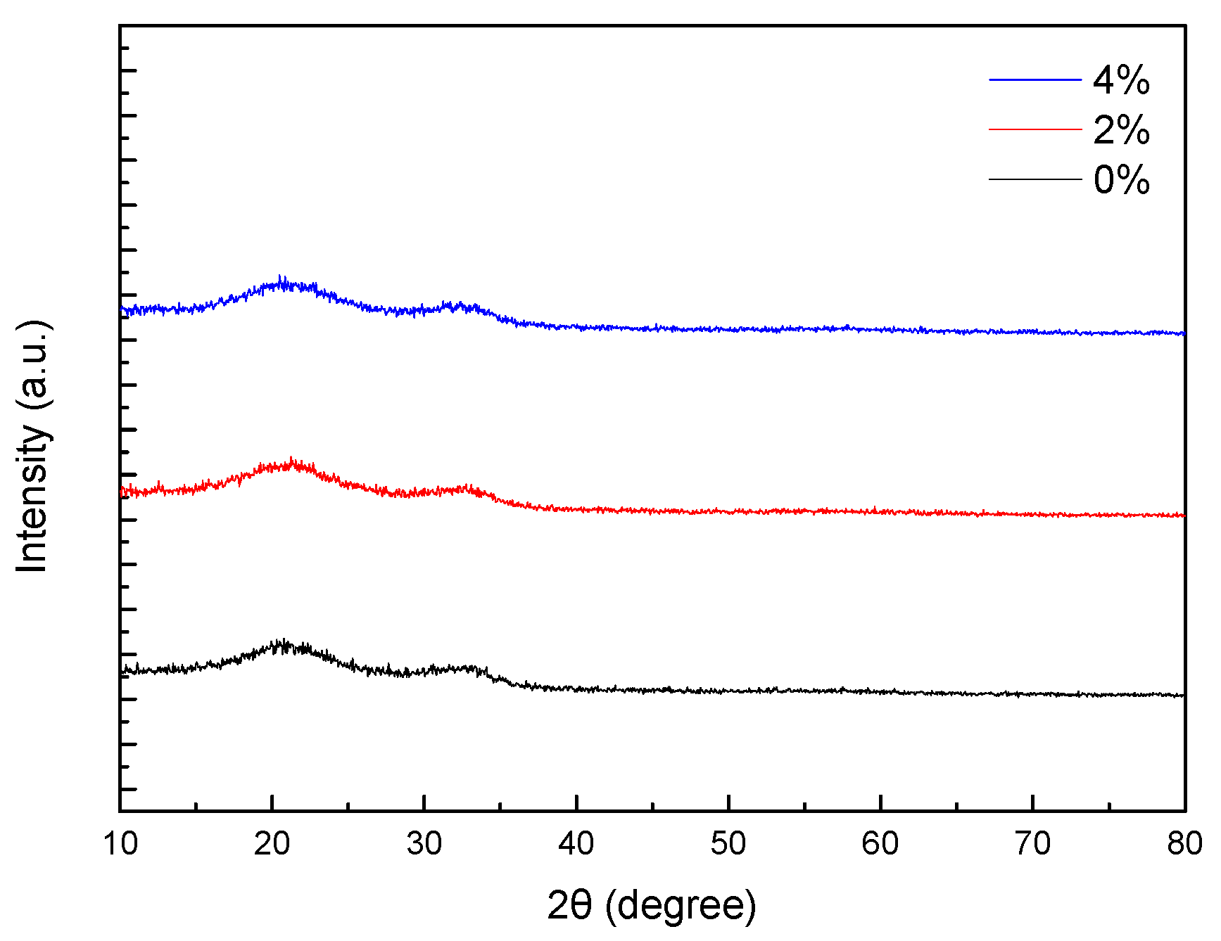
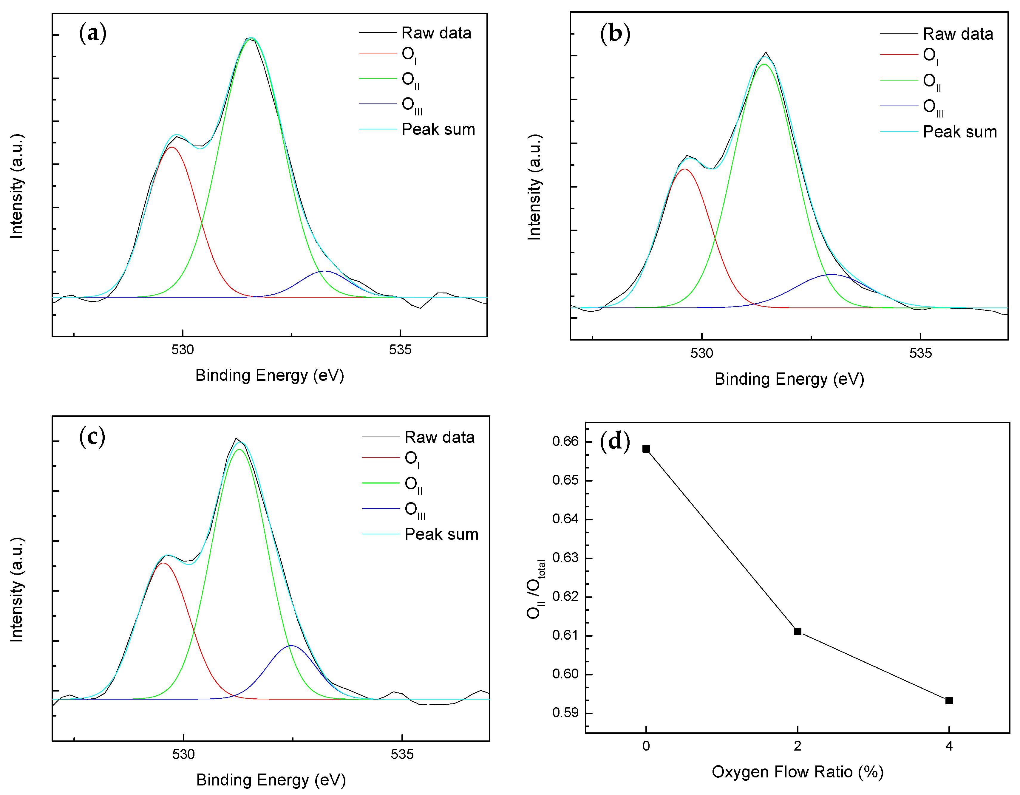
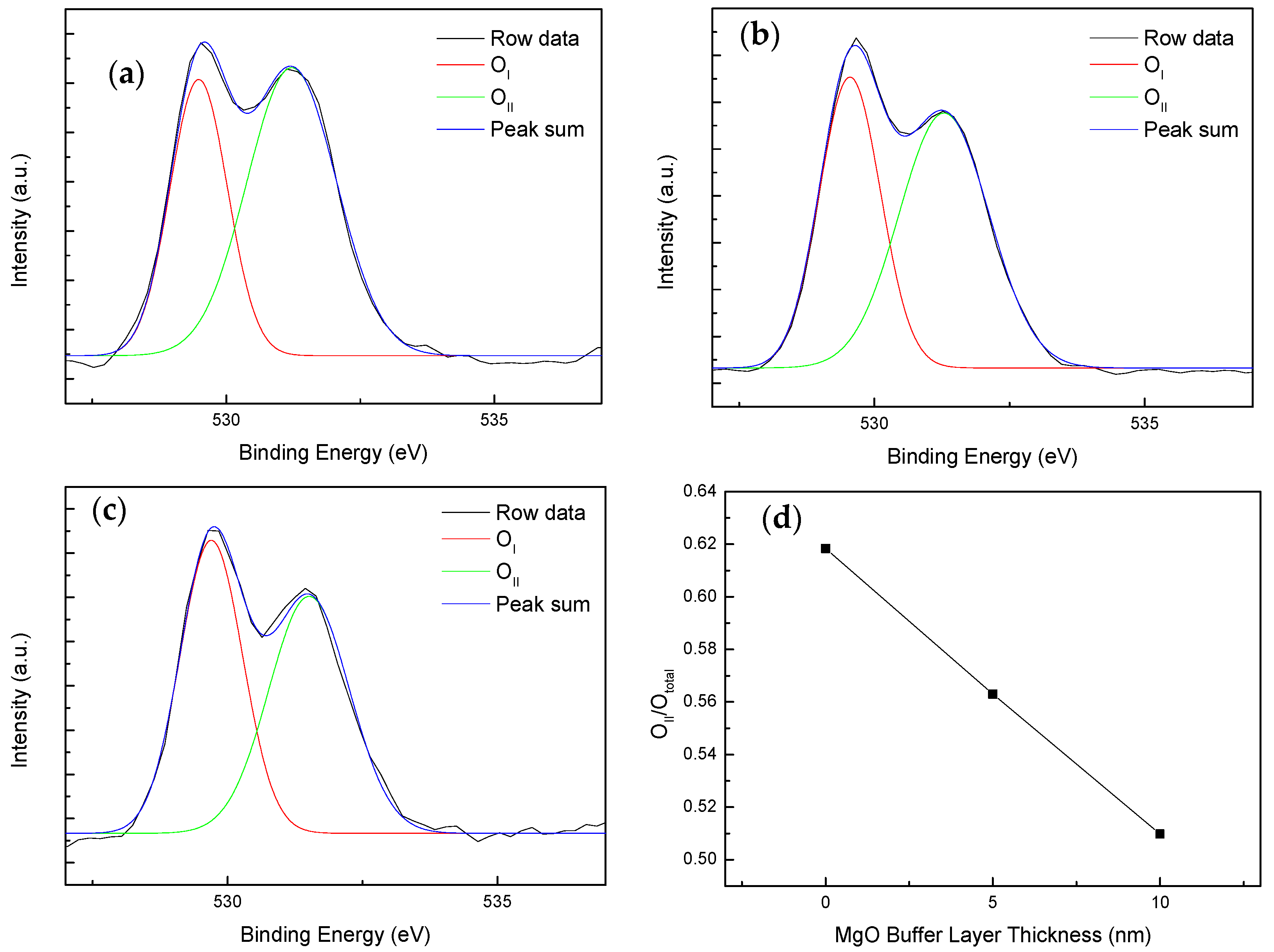
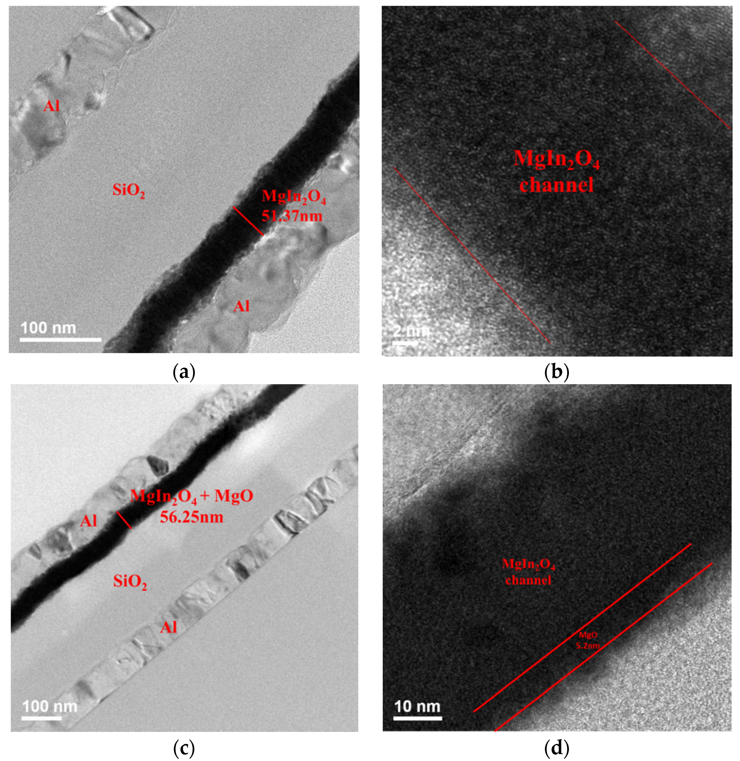
3. Results and Discussions

The XRD spectra of as-deposited 150-nm-thick MIO thin films with different oxygen partial pressures are shown in Figure 2. The slightly broad peak in the spectrum around 21.8° was due to the quartz substrate [20]. There were no remarkable peaks relevant to MgO, In2O3, and MIO, indicating those thin films are all amorphous regardless of varied oxygen flow ratios.
The oxygen vacancies in the 150-nm-thick MIO thin films were verified by XPS analysis. It is known that conductive carriers in the n-type oxide semiconductors originate from donor defects such as interstitial, substituted cations, or oxygen vacancies [21]. Oxygen vacancies are an essential issue that not only affects the carrier concentration of materials but also the stability of devices [22,23]. Figure 3 exhibits the O1s binding energy spectra of MIO thin films with different oxygen flow ratios, and the measured O1s peaks were de-convoluted into three components by utilizing Gaussian fitting carefully. The lowest-binding energy peak (OI) approximately centered at 529.6 eV originated from bonds between metal and oxygen atoms. The medium-binding energy peak (OII) centered at about 531.5 eV is related to oxygen ions in the oxygen-deficient regions in the oxide thin film, indicating the presence of oxygen vacancies. The highest-binding energy peak (OIII) was attributed to weakly bound oxygen contamination, such as absorbed COx or H2O on the surface of thin films [18,24,25]. The amounts of oxygen vacancies were compared between each MIO thin film by calculating the oxygen deficiency ratio, defined as the area under the OII curve divided by the total area, and the results are displayed in Figure 3d. It was observed that the oxygen vacancies reduced monotonically as the oxygen flow ratio increased. The oxygen tended to fill up the oxygen deficiency regions in the MIO thin films when introducing oxygen flow to the chamber during the sputtering process, resulting in fewer oxygen vacancies. This effect was even more evident when the oxygen flow further increased, as shown in the results of the XPS analysis.
The effects of adding an MgO buffer layer below the MIO thin film were also studied by XPS analysis. In order to investigate the oxygen-deficient regions in the MIO bulk, films were etched for some time before qualitative analysis. Since the films were etched in vacuum during measurement, OI and OII peaks were only taken into account for de-convoluted O1s binding energy spectra of each sample. Figure 4 shows the XPS results of MIO with different thicknesses of the MgO buffer layer. It can be clearly seen that oxygen vacancies in the MIO thin films decreased as the thickness of MgO layer increase. The result can be attributed to the diffusion of oxygen ions from MgO layer to MIO layer, which further compensated the oxygen vacancies in the channel layer.
The real deposited thickness of the device structure was verified by executing TEM analysis. Figure 5a shows cross-section TEM images of an MIO TFT, consisting of a gate electrode (Al), dielectric layer (SiO2), channel layer (MIO), and source/drain electrodes (Al). The actual thickness of the MIO thin film was close to the estimated values. The high-resolution TEM (HR-TEM) image of MIO channel layer is displayed in Figure 5b, indicating that the as-deposited MIO active layer was amorphous, which is consistent with the XRD result. Figure 5c demonstrates an MIO TFT with a 50 nm-thick MIO channel layer with an additional MgO buffer layer of 5 nm. The total thickness of the channel layer with and without the MgO buffer layer are marked in both Figure 1a,c. It is worth noting that the MIO channel layer and the MgO buffer layer had a good interface, since no obvious interface could be observed from the HR-TEM image shown in Figure 5d.
Moreover, the element composition of the MIO layer with and without an MgO buffer layer was verified by EDS analysis. Table 1 lists the elemental composition of both samples. There existed excessive amounts of oxygen in the MgO buffer layer. After the MIO thin film was deposited, the excess of oxygen could diffuse into the above layer. As a result, the amount of oxygen in the MIO thin film increased considerably, and the oxygen vacancies were suppressed, as shown in the XPS analysis.
To observe the effect of processing conditions on the electrical performance of MIO TFTs, the oxygen-to-argon flow ratios of the introduced gas varied from 0% to 4% with a step of 2% during the sputtering process. For simplification, herein we name the fabricated TFTs with the channel layers deposited in oxygen partial pressure of 0%, 2%, and 4% as sample T1, T2, and T3, respectively.
Figure 6 shows the output characteristics (ID–VD) of sample T1, T2, and T3. The drain current (ID) of each device was measured by sweeping drain voltage (VD) from 0 to 10 V with a gate voltage (VG) from 0 to 10 V in 2 V steps. It was obvious that all devices exhibited typical n-channel enhancement-mode transistor behavior and clear pinch-off and output current saturation. In the linear region, in other words, at low drain voltage region, drain current increased linearly with gate bias, owing to the charge density accumulation at the interface between the channel layer and dielectric layer.
The transfer characteristics (ID–VG) of sample T1, T2, and T3 are illustrated in Figure 6, obtained by sweeping VG from −2 V to 10 V with VD fixed at a bias of 8 V, and their representative parameters are summarized in Table 2. The threshold voltage (VT) was derived by fitting a straight line to the linear portion with maximum slop of the (ID)1/2 versus VG curve and then intercepting the line to the VG-axis. The mobility (μE) of prepared TFTs was calculated by using the equation of the saturation region, ID = (W/L)CoxμE(VG − Vth)2. Subthreshold swing (SS) was determined from the inverse slope of the linear regime of the transfer curve and could be expressed as SS = (d(logID)/dVG)−1. Interface trap density (Nit) is defined as the defect existing at the interface between the dielectric layer and the channel layer, and it is calculated by the formula, Nit = ((qSSlog(e)/kT) − 1)Cox/q.
It is clear that threshold voltage in conjunction with the oxygen flow ratios. Because oxygen vacancies, which can act as electron donors, can provide free electron carriers in the channel layer [26]. On the other hand, field-effect mobility (μE) exhibits an opposite tendency, since mobility can be increased with increased electron carrier density in oxide semiconductors [27]. All samples possessed a relatively low mobility, which is in good agreement with the reported values of MIO TFTs [28]. Although indium oxide-based TFTs usually show good mobility, doping with Mg would degrade the mobility on account of the decreased oxygen vacancies [29]. Moreover, since suppressing oxygen vacancies resulted in less bulk defect and interface trap density (Nit) in the channel layer, sample T3 showed the lowest SS. The trap density of each sample was also estimated, and sample T3 indeed possessed the lowest trap density. Additionally, sample T1 showed a lower on/off ratio due to a higher off current because of more oxygen vacancies. Moreover, sample T3 presented a lower on/off ratio owing to the inferior on-current, derived from the least carrier concentration. On the other hand, sample T2 exhibited a best on/off ratio of 8.06 × 10³. Therefore, sample T2 was assumed to be the superior device in this section.
The effects of different channel layer thickness on MIO TFTs with oxygen flow ratio fixed at 2% were further studied. The thickness of the channel layer was controlled by changing the sputtering duration. For the sake of simplicity, we named the TFTs with channel layer thicknesses of 50, 30, 20, and 10 nm as samples T2, T4, T5, and T6, respectively.
The output characteristics of samples T2, T4, T5, and T6 were measured in same way mentioned above, and those are illustrated in Figure 7. Likewise, all samples showed typical n-channel enhancement-mode transistor behavior as well as the evident pinch-off and drain current saturation.
Figure 7 displays the transfer characteristics of TFTs with different channel layer thicknesses, and the corresponding crucial parameters are also tabulated in Table 2. First, the threshold voltage increased when the thickness was decreased. Because there were fewer electron carriers in the channel layer, the TFT needed a higher voltage to accumulate carriers and turn on the device [7]. Second, field-effect electron mobility decreased with thickness due to a more serious scattering at the MIO/SiO2 interface, especially for sample T6 [30]. Third, the subthreshold swing improved distinctly with decreasing thickness. Since all samples had the same MIO/SiO2 interface, the improved SS was likely due to the lower amount of bulk trap, and thus the controlling ability of the gate was enhanced [31]. After comparison, sample T4 exhibited the best performance with a highest on/off ratio of 5.88 × 10⁴, a field-effect mobility of 0.23 cm2/V∙s, a moderate threshold voltage of 1.54 V, and a subthreshold swing of 0.61 V/decade.
Herein, the effects of different thicknesses of MgO buffer layers was studied. Figure 8 exhibits the output characteristics (ID–VD) of MIO TFTs with and without an MgO buffer layer, and all devices exhibited a typical n-channel enhancement-mode transistor behavior. The transfer characteristics of MIO TFTs with and without an MgO buffer layer are shown in Figure 8, and their representative parameters are summarized in Table 3. In the EDS analysis section, we demonstrated that there was excessive oxygen in the MgO buffer layer, and the excessive oxygen could diffuse into the channel layer. Hence, some of the oxygen vacancies in the MIO channel layer were compensated, as evidenced in XPS analysis. As a result, the carrier concentration and bulk trap density were reduced. Therefore, threshold voltage increased in conjunction with the thickness of the MgO buffer layer. On the other hand, the subthreshold swing was enhanced notably due to the suppression of oxygen vacancies in the MIO channel. Moreover, in the TEM analysis section, we also demonstrated that the MgO buffer layer showed a good interface with the MIO channel layer. Therefore, interface scattering was also improved due to the homogeneous MgO buffer layer, which matched the channel lattice better compared to SiO2. Hence, the mobility of MIO TFT with a 5 nm MgO buffer layer increased over ten times.
However, with a view to the MIO TFT with a 10 nm MgO buffer layer, the oxygen vacancies were suppressed even more strongly. and this degraded its mobility as well as the on/off current ratio due to severe decreases of the carrier concentration. Although its subthreshold swing was much better than that of TFT with a 5 nm MgO buffer layer, it also exhibited an undesirable higher threshold voltage. As a consequence, MIO TFT, with a 5 nm MgO buffer layer, showed the best performance with the highest on/off current ratio of 9.68 × 10³, a field-effect mobility of 4.81 cm2/V∙s, a threshold voltage of 2.01 V, and a subthreshold swing of 0.76 V/decade.

4. Conclusions

In this study, an MIO thin film transistor was fabricated on a quartz substrate by an RF sputter system under different oxygen flow ratios. The optimized parameters of the MIO TFT are oxygen flow ratio of 2% and thickness of 30 nm, which show the highest on/off ratio of 5.88×10⁴, field-effect mobility of 0.23 cm2/V∙s, a moderate threshold voltage of 1.54 V, and a subthreshold swing of 0.61 V/decade. In addition, an MIO TFT with an MgO buffer layer of 5 nm was demonstrated. The MgO buffer layer provides a good interface with the channel layer. Due to the excessive oxygen from the buffer layer, the oxygen vacancies in the MIO channel layer can be suppressed, and the mobility is then improved. As a result, MIO TFT with a 5 nm MgO buffer layer shows an on/off current ratio of 9.68 × 10³, field-effect mobility of 4.81 cm2/V∙s, a threshold voltage of 2.01 V, and a subthreshold swing of 0.76 V/decade. In conclusion, the proper material between the oxide layer and the channel layer may improve the interface and further enhance the performance.

Author Contributions

Conceptualization, methodology, and writing—original draft preparation, W.-D.C. and S.-P.C.; Writing—review and editing, W.-D.C., and W.-L.H.; Supervision, S.-P.C.; Conceptualization and methodology, S.-P.C. and W.-L.H. All authors have read and agreed to the published version of the manuscript.

Funding

This research was funded by the Ministry of Science and Technology of the Republic of China (ROC) under grant number 107-2221-E-006-189-MY3 and 109-2221-E-006-203-MY3.

Conflicts of Interest

The authors declare no conflict of interest.

References

  1. Nomura, K.; Ohta, H.; Takagi, A.; Kamiya, T.; Hirano, M.; Hosono, H. Room-temperature fabrication of transparent flexible thin-film transistors using amorphous oxide semiconductors. Nature 2004, 432, 488–492. [Google Scholar] [CrossRef] [PubMed]
  2. Fortunato, E.M.C.; Barquinha, P.M.C.; Pimentel, A.C.M.B.G.; Gonçalves, A.M.F.; Marques, A.J.S.; Pereira, L.M.N.; Martins, R.F.P. Fully transparent ZnO thin-film transistor produced at room temperature. Adv. Mater. 2005, 17, 590–594. [Google Scholar] [CrossRef]
  3. Jang, Y.K.; Kyoung, S.S.; Ji, S.J.; Tae, S.K.; Myung, K.R.; Kyung, B.P.; Byung, W.Y.; Jung, W.Y.; Young, G.L.; Kee, C.P.; et al. Bottom-gate gallium indium zinc oxide thin-film transistor array for high-resolution AMOLED display. IEEE Electron. Device Lett. 2008, 29, 1309–1311. [Google Scholar]
  4. Lee, S.; Arokia, N. Subthreshold Schottky-barrier thin-film transistors with ultralow power and high intrinsic gain. Science 2016, 354, 302–304. [Google Scholar] [CrossRef] [PubMed] [Green Version]
  5. Faber, H.; Das, S.; Lin, Y.H.; Pliatsikas, N.; Zhao, K.; Kehagias, T.; Dimitrakopulos, G.; Amassian, A.; Patsalas, P.A.; Anthopoulos, T.D. Heterojunction oxide thin-film transistors with unprecedented electron mobility grown from solution. Sci. Adv. 2017, 3, e1602640. [Google Scholar] [CrossRef] [PubMed] [Green Version]
  6. Wu, C.; Li, X.; Lu, J.; Ye, Z.; Zhang, J.; Zhou, T.; Sun, R.; Chen, L.; Lu, B.; Pan, X. Characterization of amorphous Si-Zn-Sn-O thin films and applications in thin-film transistors. Appl. Phys. Lett. 2013, 103, 082109. [Google Scholar] [CrossRef]
  7. Noh, J.H.; Ryu, S.Y.; Jo, S.J.; Kim, C.S.; Sohn, S.W.; Rack, P.D.; Kim, D.J.; Baik, H.K. Indium oxide thin-film transistors fabricated by RF sputtering at room temperature. IEEE Electron. Device Lett. 2010, 31, 567–569. [Google Scholar]
  8. Kim, Y.G.; Kim, T.; Avis, C.; Lee, S.H.; Jang, J. Stable and high-performance indium oxide thin-film transistor by Ga doping. IEEE Trans. Electron. Devices 2016, 63, 1078–1084. [Google Scholar] [CrossRef]
  9. Luo, Y.R. Comprehensive Handbook of Chemical Bond. Energies; CRC Press: New York, NY, USA, 2007; pp. 9-65–9-70. [Google Scholar]
  10. Barbalace, K. “Periodic Table of Elements”. Environmental Chemistry.com 2007, 04–14. Available online: https://environmentalchemistry.com/ (accessed on 20 December 2020).
  11. Koide, H.; Nagao, Y.; Koumoto, K.; Takasaki, Y.; Umemura, T.; Kato, T.; Ikuhara, Y.; Ohta, H. Electric field modulation of thermopower for transparent amorphous oxide thin film transistors. Appl. Phys. Lett. 2010, 97, 182105. [Google Scholar] [CrossRef] [Green Version]
  12. Luka, G.; Krajewski, T.A.; Witkowski, B.S.; Wisz, G.; Virt, I.S.; Guziewicz, E.; Godlewski, M. Aluminum-doped zinc oxide films grown by atomic layer deposition for transparent electrode applications. J. Mater. Sci. Mater. Electron. 2011, 22, 1810–1815. [Google Scholar] [CrossRef] [Green Version]
  13. Zhan, R.; Dong, C.; Liu, P.T.; Shieh, H.P.D. Influence of channel layer and passivation layer on the stability of amorphous InGaZnO thin film transistors. Microelectron. Reliab. 2013, 53, 1879–1885. [Google Scholar] [CrossRef]
  14. Wu, C.H.; Chang, K.M.; Huang, S.H.; Deng, I.C.; Wu, C.J.; Chiang, W.H.; Chang, C.C. Characteristics of IGZO TFT Prepared by Atmospheric Pressure Plasma Jet Using PE-ALD Al2O3 Gate Dielectric. IEEE Electron. Device Lett. 2012, 33, 552–554. [Google Scholar] [CrossRef]
  15. Liu, G.X.; Liu, A.; Shan, F.K.; Meng, Y.; Shin, B.C.; Fortunato, E.; Martins, R. High-performance fully amorphous bilayer metal-oxide thin film transistors using ultra-thin solution-processed ZrOx dielectric. Appl. Phys. Lett. 2014, 105, 113509. [Google Scholar] [CrossRef]
  16. Na, S.Y.; Kim, Y.M.; Yoon, D.J.; Yoon, S.M. Improvement in negative bias illumination stress stability of In-Ga-Zn-O thin film transistors using HfO2 gate insulators by controlling atomic-layer-deposition conditions. J. Phys. D Appl. Phys. 2017, 50, 495109. [Google Scholar] [CrossRef]
  17. Jiang, G.; Liu, A.; Liu, G.; Zhu, C.; Meng, Y.; Shin, B.; Fortunato, E.; Martins, R.; Shan, F. Solution-processed high-κ magnesium oxide dielectrics for low-voltage oxide thin-film transistors. Appl. Phys. Lett. 2016, 109, 183508. [Google Scholar] [CrossRef]
  18. Lee, J.H.; Kim, H.S.; Kim, S.H.; Jang, N.W.; Yun, Y. Characterization of magnesium oxide gate insulators grown using RF sputtering for ZnO thin-film transistors. Curr. Appl. Phys. 2014, 14, 794–797. [Google Scholar] [CrossRef]
  19. Huang, H.Q.; Liu, F.J.; Sun, J.; Zhao, J.W.; Hu, Z.F.; Li, Z.J.; Zhang, X.Q.; Wang, Y.S. Effect of MgO buffer layer thickness on the electrical properties of MgZnO thin film transistors fabricated by plasma assisted molecular beam epitaxy. Appl. Surf. Sci. 2011, 257, 10721–10724. [Google Scholar] [CrossRef]
  20. Dai, S.; Wang, T.; Li, R.; Wang, Q.; Ma, Y.; Tian, L.; Su, J.; Wang, Y.; Zhou, D.; Zhang, X.; et al. Preparation and electrical properties of N-doped ZnSnO thin film transistors. J. Alloys Compd. 2018, 745, 256–261. [Google Scholar] [CrossRef]
  21. Dali, S.E.; Chockalingam, M.J. Combustion synthesis of magnesium indate, MgIn2O4. Mater. Chem. Phys. 2001, 70, 73–77. [Google Scholar] [CrossRef]
  22. Jeon, H.J.; Maeng, W.J.; Park, J.S. Effect of Al concentration on the electrical characteristics of solution-processed Al doped ZnSnO thin film transistors. Ceram. Int. 2014, 40, 8769–8774. [Google Scholar] [CrossRef]
  23. Lee, K.H.; Ok, K.C.; Kim, H.; Park, J.S. The influence of oxygen partial pressure on the performance and stability of Ge-doped InGaO thin film transistors. Ceram. Int. 2014, 40, 3215–3220. [Google Scholar] [CrossRef]
  24. Liu, L.C.; Chen, J.S.; Jeng, J.S. Role of oxygen vacancies on the bias illumination stress stability of solution-processed zinc tin oxide thin film transistors. Appl. Phys. Lett. 2014, 105, 023509. [Google Scholar] [CrossRef]
  25. Li, J.; Huang, C.X.; Zhang, J.H.; Zhu, W.Q.; Jiang, X.Y.; Zhang, Z.L. Characterization of novel BaZnSnO thin films by solution process and applications in thin film transistors. Mater. Res. Bull. 2015, 68, 22–26. [Google Scholar] [CrossRef]
  26. Choi, S.; Kim, J.Y.; Kang, H.; Ko, D.; Rhee, J.; Choi, S.J.; Kim, D.M.; Kim, D.H. Effect of oxygen content on current stress-induced instability in bottom-gate amorphous InGaZnO thin-film transistors. Materials 2019, 12, 3149. [Google Scholar] [CrossRef] [PubMed] [Green Version]
  27. Yao, J.; Xu, N.; Deng, S.; Chen, J.; She, J.; Shieh, H.P.D.; Liu, P.T.; Haung, Y.P. Electrical and photosensitive characteristics of a-IGZO TFTs related to oxygen vacancy. IEEE Trans. Electron. Devices 2011, 58, 1121–1126. [Google Scholar]
  28. Lu, H.; Bi, X.; Zhang, S.; Zhou, H. Ultraviolet detecting properties of amorphous MgInO thin film phototransistors. Semicond. Sci. Technol. 2015, 30, 125010. [Google Scholar] [CrossRef]
  29. Lu, H.; Zhou, X.; Liang, T.; Zhang, L.; Zhang, S. Oxide thin-film transistors with IMO and IGZO stacked active layers for UV detection. IEEE J. Electron. Devices Soc. 2017, 5, 504–508. [Google Scholar] [CrossRef]
  30. Chen, A.H.; Cao, H.T.; Zhang, H.Z.; Liang, L.Y.; Liu, Z.M.; Yu, Z.; Wan, Q. Influence of the channel layer thickness on electrical properties of indium zinc oxide thin-film transistor. Microelectron. Eng. 2010, 87, 2019–2023. [Google Scholar] [CrossRef]
  31. Yang, Z.; Yang, J.; Meng, T.; Qu, M.; Zhang, Q. Influence of channel layer thickness on the stability of amorphous indium zinc oxide thin film transistors. Mater. Lett. 2016, 166, 46–50. [Google Scholar] [CrossRef]
Figure 1. Schematic structure of (a) the MgIn2O4 thin film transistor (MIO TFT) and (b) the MIO TFT with an MgO buffer layer.
Coatings 10 01261 g001
Figure 2. XRD spectra of MIO thin films with different oxygen flow ratios.
Coatings 10 01261 g002
Figure 3. XPS O1s spectra of MIO thin films with various oxygen flow ratios: (a) 0%, (b) 2%, (c) 4%, (d) OII/Ototal ratios of MIO thin films with various oxygen flow ratios.
Coatings 10 01261 g003
Figure 4. XPS O1s spectra of MIO thin films (a) without MgO buffer layer, (b) with 5 nm-thick MgO buffer layer, (c) with 10 nm-thick MgO buffer layer, (d) OII/Ototal ratios of MIO thin films with various thickness of MgO buffer layer.
Coatings 10 01261 g004
Figure 5. (a) Cross-section TEM and (b) HR-TEM images of the MIO TFT; (c) cross-section TEM and (d) HR-TEM image of the MIO TFT with MgO buffer layer.
Coatings 10 01261 g005
Figure 6. Output characteristics of MIO TFTs with different oxygen-to-argon flow ratios: (a) sample T1, (b) sample T2, (c) sample T3. Transfer characteristics of MIO TFTs with different oxygen-to-argon flow ratios: (d) sample T1, (e) sample T2, (f) sample T3.
Coatings 10 01261 g006
Figure 7. Output characteristics of MIO TFTs with various channel layer thicknesses: (a) sample T2, (b) sample T4, (c) sample T5, (d) sample T6. Transfer characteristics of MIO TFTs with channel active layer thicknesses: (e) sample T2, (f) sample T4, (g) sample T5, (h) sample T6.
Coatings 10 01261 g007aCoatings 10 01261 g007b
Figure 8. Output characteristics of MIO TFTs (a) without buffer layer, (b) with 5 nm buffer layer, and (c) 10 nm buffer layer, and transfer characteristics of MIO TFTs (d) without buffer layer, (e) with a 5 nm MgO buffer layer, and (f) with a 10 nm MgO buffer layer.
Coatings 10 01261 g008
Table 1. Element composition (at.%) of MIO channel with and without the MgO buffer layer, and element composition of MgO buffer layer. N/A means we are only concerned about the amounts of Mg and O in the MgO layer.
ElementMIO
without MgO Layer
MIO
with 5 nm MgO
MgO
Buffer Layer
Mg11.39%11.44%26.84%
In41.84%31.44%N/A
O46.76%57.12%73.16%
Mg/In0.270.36N/A
Table 2. Transfer characteristics of MIO TFTs with different oxygen-to-argon flow ratios or channel thicknesses.
MIO
TFT
Oxygen
Partial
Pressure
MIO
Thickness
(nm)
VT
(V)
μE
(cm2/V∙s)
On/Off
Ratio
SS
(V/dec)
Nit
(cm−2)
T10%500.970.341.49 × 1031.011.72 × 1012
T22%501.150.298.06 × 1030.771.28 × 1012
T34%502.340.023.35 × 1030.701.17 × 1012
T42%301.540.235.88 × 1040.61N/A
T52%201.690.232.15 × 1040.59N/A
T62%102.520.061.52 × 1040.46N/A
Table 3. Transfer characteristics of MIO TFTs with and without MgO buffer layer.
MgO
Thickness
(nm)
VT
(V)
μE
(cm2/V∙s)
On/Off
Ratio
SS
(V/dec)
Nit
(cm−2)
00.970.341.49 × 1031.011.72 × 1012
52.014.819.68 × 1030.761.27 × 1012
103.063.322.58 × 1030.691.14 × 1012
Publisher’s Note: MDPI stays neutral with regard to jurisdictional claims in published maps and institutional affiliations.

