Influence of N2 Gas Flow Ratio and Working Pressure on Amorphous Mo–Si–N Coating during Magnetron Sputtering


Abstract
:1. Introduction
2. Experimental
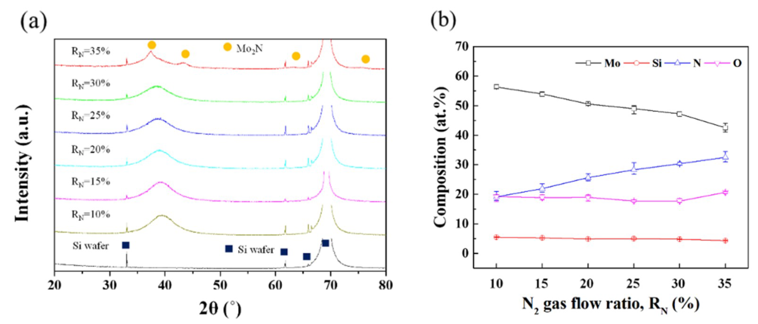
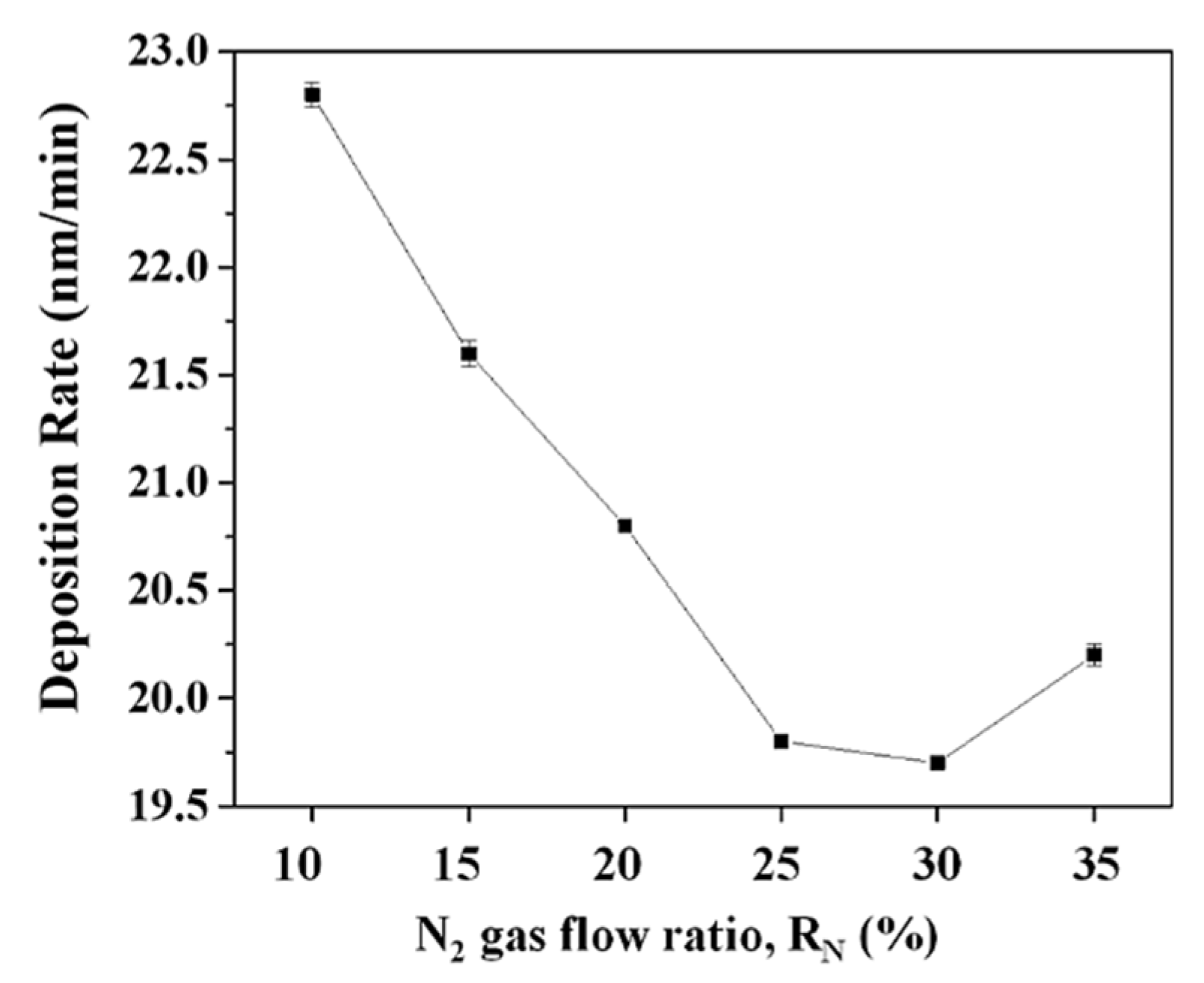
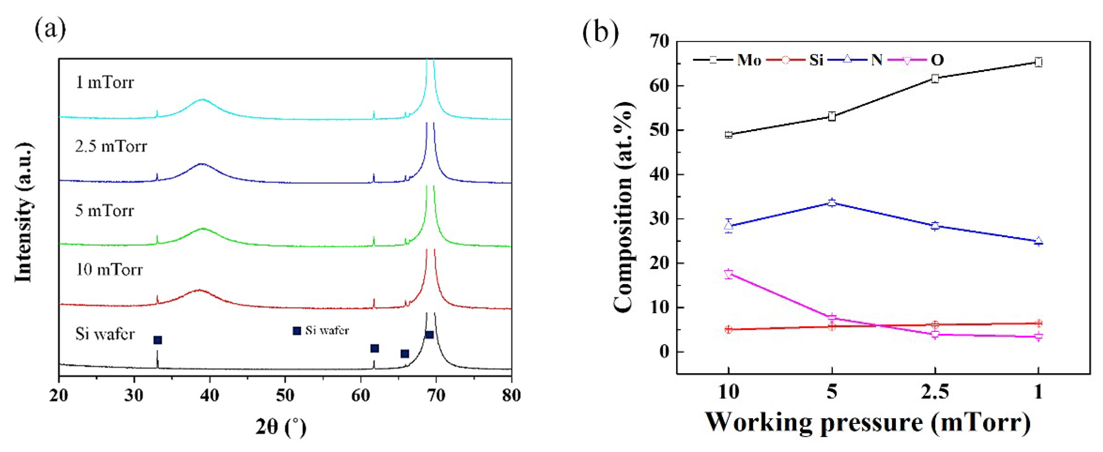
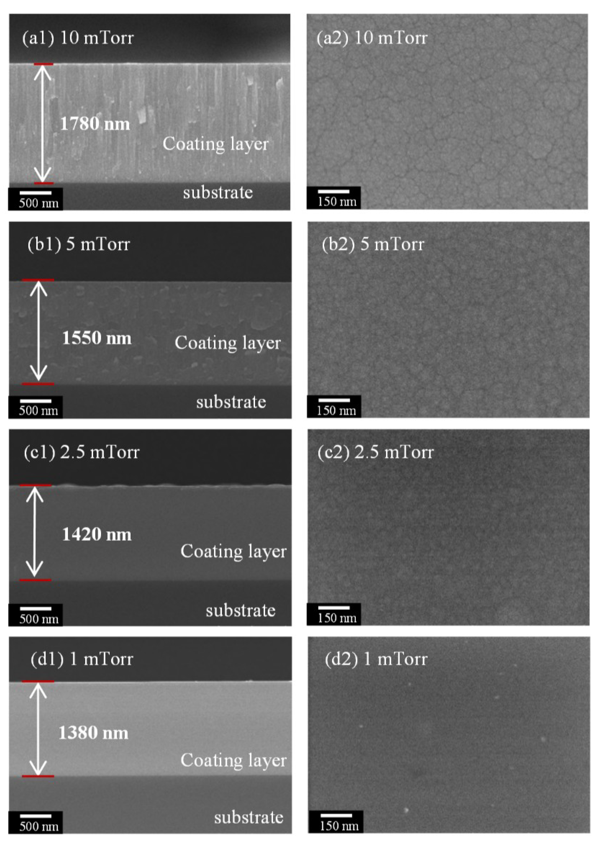
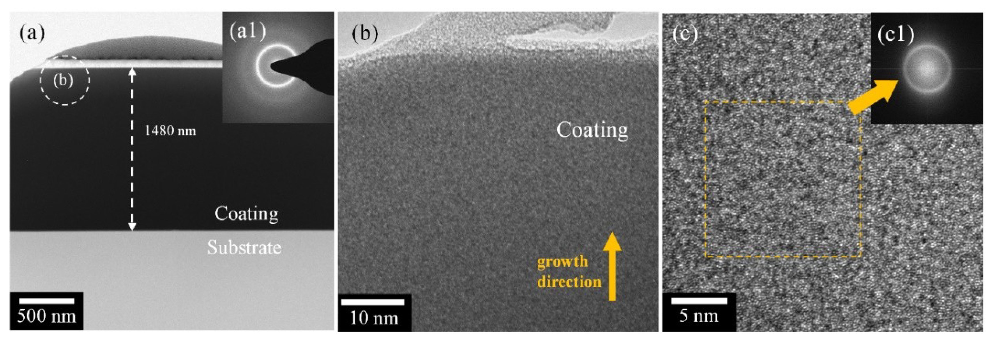
3. Results and Discussion
4. Conclusions
Author Contributions
Funding
Conflicts of Interest
References
- Hones, P.; Martin, N.; Regula, M.; Lévy, F. Structural and mechanical properties of chromium nitride, molybdenum nitride, and tungsten nitride thin films. J. Phys. D: Appl. Phys. 2003, 36, 1023. [Google Scholar] [CrossRef]
- Kazmanli, M.; Ürgen, M.; Cakir, A. Effect of nitrogen pressure, bias voltage and substrate temperature on the phase structure of Mo–N coatings produced by cathodic arc PVD. Surf. Coat. Technol. 2003, 167, 77–82. [Google Scholar] [CrossRef]
- Heo, S.J.; Kim, K.H.; Kang, M.C.; Suh, J.H.; Park, C.-G. Syntheses and mechanical properties of Mo–Si–N coatings by a hybrid coating system. Sur. Coat. Technol. 2006, 201, 4180–4184. [Google Scholar] [CrossRef]
- Wang, Y.; Lin, R.Y. Amorphous molybdenum nitride thin films prepared by reactive sputter deposition. Mater. Sci. Eng. B. 2004, 112, 42–49. [Google Scholar] [CrossRef]
- Öztürk, A.; Ezirmik, K.; Kazmanlı, K.; Ürgen, M.; Eryılmaz, O.; Erdemir, A. Comparative tribological behaviors of TiN, CrN and MoN Cu nanocomposite coatings. Tribol. Int. 2008, 41, 49–59. [Google Scholar] [CrossRef]
- Xiang, J.; Lin, Z.; Renoux, E.; Wu, F. Microstructure evolution and indentation cracking behavior of MoN multilayer films. Surf. Coat. Technol. 2018, 350, 1020–1027. [Google Scholar] [CrossRef]
- Ürgen, M.; Eryilmaz, O.; Çakir, A.; Kayali, E.; Nilüfer, B.; Işik, Y. Characterization of molybdenum nitride coatings produced by arc-PVD technique. Surf. Coat. Technol. 1997, 94, 501–506. [Google Scholar] [CrossRef]
- Chuang, J.-C.; Tu, S.-L.; Chen, M.-C. Sputter-deposited Mo and reactively sputter-deposited Mo–N films as barrier layers against Cu diffusion. Thin Solid Films 1999, 346, 299–306. [Google Scholar] [CrossRef]
- Nicolet, M.-A.; Giauque, P. Highly metastable amorphous or near-amorphous ternary films (mictamict alloys). Microelectron. Eng. 2001, 55, 357–367. [Google Scholar] [CrossRef]
- Hirvonen, J.-P.; Suni, I.; Kattelus, H.; Lappalainen, R.; Torri, P.; Kung, H.; Jervis, T.; Nastasi, M.; Tesmer, J. Crystallization and oxidation behavior of Mo–Si–N coatings. Surf. Coat. Technol. 1995, 74, 981–985. [Google Scholar] [CrossRef]
- Liu, Q.; Fang, Q.; Liang, F.; Wang, J.; Yang, J.; Li, C. Synthesis and properties of nanocomposite MoSiN hard films. Surf. Coat. Technol. 2006, 201, 1894–1898. [Google Scholar] [CrossRef]
- Musil, J.; Dohnal, P.; Zeman, P. Physical properties and high-temperature oxidation resistance of sputtered Si3N4∕MoNx nanocomposite coatings. J. Vac. Sci. Technol. B. 2005, 23, 1568–1575. [Google Scholar] [CrossRef]
- Tsai, D.-C.; Huang, Y.-L.; Lin, S.-R.; Liang, S.-C.; Shieu, F.-S. Effect of nitrogen flow ratios on the structure and mechanical properties of (TiVCrZrY)N coatings prepared by reactive magnetron sputtering. Appl. Surf. Sci. 2010, 257, 1361–1367. [Google Scholar] [CrossRef]
- Tsai, D.-C.; Chang, Z.-C.; Kuo, B.-H.; Chen, B.-C.; Chen, E.-C.; Shieu, F.-S. Wide variation in the structure and physical properties of reactively sputtered (TiZrHf)N coatings under different working pressures. J. Alloy. Compd. 2018, 750, 350–359. [Google Scholar] [CrossRef]
- Thornton, J.A. Influence of apparatus geometry and deposition conditions on the structure and topography of thick sputtered coatings. J. Vac. Sci. Technol. 1974, 11, 666–670. [Google Scholar] [CrossRef]
- Xu, Y.; Cui, J.; Cui, H.; Zhou, H.; Yang, Z.; Du, J. Influence of deposition pressure, substrate temperature and substrate outgassing on sorption properties of Zr–Co–Ce getter films. J. Alloy. Compd. 2016, 661, 396–401. [Google Scholar] [CrossRef]
- Xiang, J.-Y.; Wu, F.-B. Gas inlet and input power modulated sputtering molybdenum nitride thin films. Surf. Coat. Technol. 2017, 332, 161–167. [Google Scholar] [CrossRef]
- Yan, W.; Pun, C.L.; Simon, G.P. Conditions of applying Oliver–Pharr method to the nanoindentation of particles in composites. Compos. Sci. Technol. 2012, 72, 1147–1152. [Google Scholar] [CrossRef]
- Bull, S. Nanoindentation of coatings. J. Phys. D: Appl. Phys. 2005, 38, R393. [Google Scholar] [CrossRef]
- Kim, Y.S.; Park, H.J.; Mun, S.C.; Jumaev, E.; Hong, S.H.; Song, G.; Kim, J.T.; Park, Y.K.; Kim, K.S.; Jeong, S.I. Investigation of structure and mechanical properties of TiZrHfNiCuCo high entropy alloy thin films synthesized by magnetron sputtering. J. Alloy. Compd. 2019, 797, 834–841. [Google Scholar] [CrossRef]
- Kattelus, H.; Koskenala, J.; Nurmela, A.; Niskanen, A. Stress control of sputter-deposited Mo–N films for micromechanical applications. Microelectronic Eng. 2002, 60, 97–105. [Google Scholar] [CrossRef]
- French, B.; Bilello, J. In situ observations of the real-time stress-evolution and delamination of thin Ta films on Si (100). Thin Solid Films 2004, 446, 91–98. [Google Scholar] [CrossRef]
- Mason, R.S.; Pichilingi, M. Sputtering in a glow discharge ion source-pressure dependence: theory and experiment. J. Phys. D: Appl. Phys. 1994, 27, 2363. [Google Scholar] [CrossRef]
- Tsau, C.-H.; Chang, Y.-H. Microstructures and mechanical properties of TiCrZrNbNx alloy nitride thin films. Entropy 2013, 15, 5012–5021. [Google Scholar] [CrossRef]
- Shi, Y.; Pan, F.; Bao, M.; Yang, Z.; Wang, L. Effect of N2 flow rate on structure and property of ZrNbAlNx multilayer films deposited by magnetron sputtering. J. Alloy. Compd. 2013, 559, 196–202. [Google Scholar] [CrossRef]
- Anitha, V.; Major, S.; Chandrashekharam, D.; Bhatnagar, M. Deposition of molybdenum nitride thin films by rf reactive magnetron sputtering. Surf. Coat. Technol. 1996, 79, 50–54. [Google Scholar] [CrossRef]
- Liu, L.; Zhu, J.; Hou, C.; Li, J.; Jiang, Q. Dense and smooth amorphous films of multicomponent FeCoNiCuVZrAl high-entropy alloy deposited by direct current magnetron sputtering. Mater. Design. 2013, 46, 675–679. [Google Scholar] [CrossRef]
- Hsueh, H.-T.; Shen, W.-J.; Tsai, M.-H.; Yeh, J.-W. Effect of nitrogen content and substrate bias on mechanical and corrosion properties of high-entropy films (AlCrSiTiZr)100−xNx. Surf. Coat. Technol. 2012, 206, 4106–4112. [Google Scholar] [CrossRef]
- Musil, J.; Kunc, F.; Zeman, H.; Polakova, H. Relationships between hardness, Young’s modulus and elastic recovery in hard nanocomposite coatings. Surf. Coat. Technol. 2002, 154, 304–313. [Google Scholar] [CrossRef]
- Leyland, A.; Matthews, A. On the significance of the H/E ratio in wear control: a nanocomposite coating approach to optimised tribological behaviour. Wear 2000, 246, 1–11. [Google Scholar] [CrossRef]
- Musil, J. Hard nanocomposite coatings: Thermal stability, oxidation resistance and toughness. Surf. Coat. Technol. 2012, 207, 50–65. [Google Scholar] [CrossRef]
- Qi, Z.; Wu, Z.; Zhang, D.; Wei, B.; Wang, J.; Wang, Z. Effect of sputtering power on the chemical composition, microstructure and mechanical properties of CrNx hard coatings deposited by reactive magnetron sputtering. Vacuum 2017, 145, 136–143. [Google Scholar] [CrossRef]
- Blinkov, I.; Chernogor, A.; Volkhonskii, A.; Sergevnin, V.; Belov, D.; Sargaeva, O. Phase composition, structure, and mechanical properties of arc PVD Mo–Si–Al and Mo–Si–Al–N coatings. Inorg. Mater. 2017, 53, 125–134. [Google Scholar] [CrossRef]
- Moon, Y.-K.; Bang, B.; Kim, S.-H.; Jeong, C.-O.; Park, J.-W. Effects of working pressure on the electrical and optical properties of aluminum-doped zinc oxide thin films. J. Mater. Sci. Mater. Electron. 2008, 19, 528–532. [Google Scholar] [CrossRef]
- Clemens, B. Effect of sputtering pressure on the structure and solid-state reaction of titanium-nickel compositionally modulated film. J. Appl. Phys. 1987, 61, 4525–4529. [Google Scholar] [CrossRef]
- Kim, K.; Das, J.; Venkataraman, S.; Yi, S.; Eckert, J. Work hardening ability of ductile Ti45Cu40Ni7.5Zr5Sn2.5 and Cu47.5Zr47.5Al5 bulk metallic glasses. Appl. Phys. Lett. 2006, 89, 071908. [Google Scholar] [CrossRef]


| Process Parameter | Values (N2 Gas Flow Ratio) | Values (Working Pressure) |
|---|---|---|
| Base pressure (Torr) | <(5.0 × 10⁻⁶) | |
| Input power (W) | D.C 300 | |
| N2 gas flow ratio (%) | 10, 15, 20, 25, 30, 35 | 25 |
| Working pressure (mTorr) | 10 | 10, 5, 2.5, 1 |
| Deposition time (min) | 90 | |
| Rotation speed (rpm) | 10 | |
| Deposition temperature | Room temperature | |
| N2 Gas Flow Ratio (%) | Mechanical Properties | ||
|---|---|---|---|
| Hardness (GPa) | Elastic Modulus (GPa) | H/E Ratio | |
| 10 | 7.4 ± 0.09 | 149.0 ± 3.34 | 0.050 ± 0.0015 |
| 15 | 9.6 ± 0.14 | 156.5 ± 2.54 | 0.061 ± 0.0013 |
| 20 | 9.8 ± 0.11 | 157.7 ± 4.70 | 0.062 ± 0.0021 |
| 25 | 9.9 ± 0.23 | 158.8 ± 3.13 | 0.062 ± 0.0020 |
| 30 | 9.1 ± 0.17 | 156.4 ± 5.55 | 0.058 ± 0.0011 |
| 35 | 7.2 ± 0.14 | 145.3 ± 3.38 | 0.050 ± 0.0010 |
| Working Pressure (mTorr) | Mechanical Properties | ||
|---|---|---|---|
| Hardness (GPa) | Elastic Modulus (GPa) | H/E Ratio | |
| 10 | 9.9 ± 0.23 | 158.8 ± 3.13 | 0.062 ± 0.0020 |
| 5 | 12.7 ± 0.17 | 194.1 ± 5.20 | 0.065 ± 0.0022 |
| 2.5 | 16.9 ± 0.29 | 208.0 ± 2.18 | 0.082 ± 0.0014 |
| 1 | 17.9 ± 0.19 | 216.1 ± 2.90 | 0.083 ± 0.0017 |
© 2020 by the authors. Licensee MDPI, Basel, Switzerland. This article is an open access article distributed under the terms and conditions of the Creative Commons Attribution (CC BY) license (http://creativecommons.org/licenses/by/4.0/).
Share and Cite
Lim, K.S.; Kim, Y.S.; Hong, S.H.; Song, G.; Kim, K.B. Influence of N2 Gas Flow Ratio and Working Pressure on Amorphous Mo–Si–N Coating during Magnetron Sputtering. Coatings 2020, 10, 34. https://doi.org/10.3390/coatings10010034
Lim KS, Kim YS, Hong SH, Song G, Kim KB. Influence of N2 Gas Flow Ratio and Working Pressure on Amorphous Mo–Si–N Coating during Magnetron Sputtering. Coatings. 2020; 10(1):34. https://doi.org/10.3390/coatings10010034
Chicago/Turabian StyleLim, Ki Seong, Young Seok Kim, Sung Hwan Hong, Gian Song, and Ki Buem Kim. 2020. "Influence of N2 Gas Flow Ratio and Working Pressure on Amorphous Mo–Si–N Coating during Magnetron Sputtering" Coatings 10, no. 1: 34. https://doi.org/10.3390/coatings10010034
APA StyleLim, K. S., Kim, Y. S., Hong, S. H., Song, G., & Kim, K. B. (2020). Influence of N2 Gas Flow Ratio and Working Pressure on Amorphous Mo–Si–N Coating during Magnetron Sputtering. Coatings, 10(1), 34. https://doi.org/10.3390/coatings10010034