Introducing Well-Defined Nanowrinkles in CVD Grown Graphene


Abstract
1. Introduction
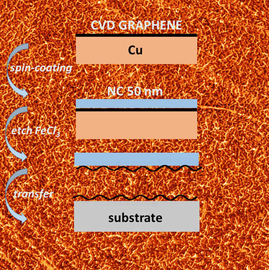
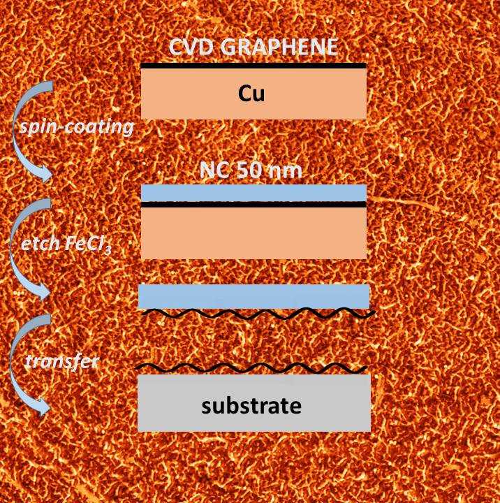
2. Materials and Methods
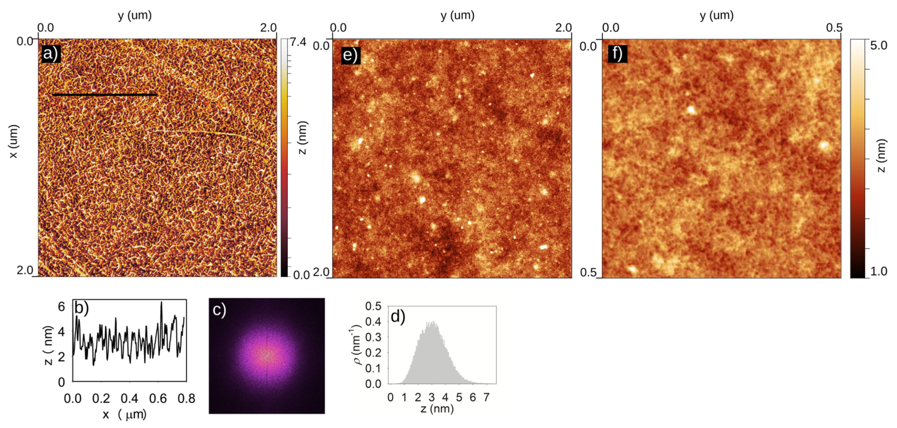
3. Results
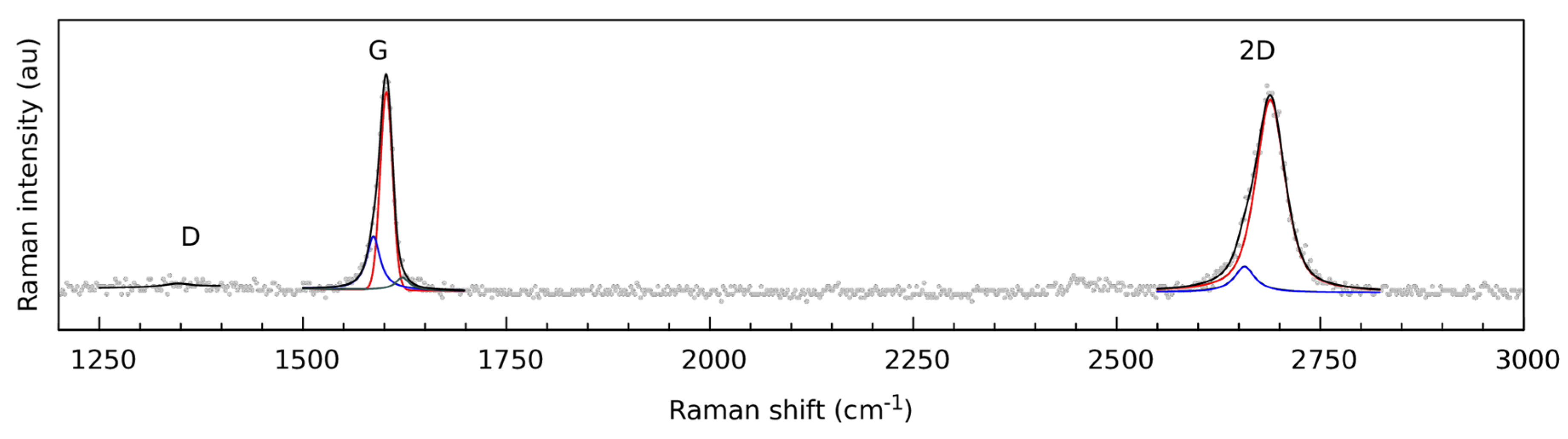
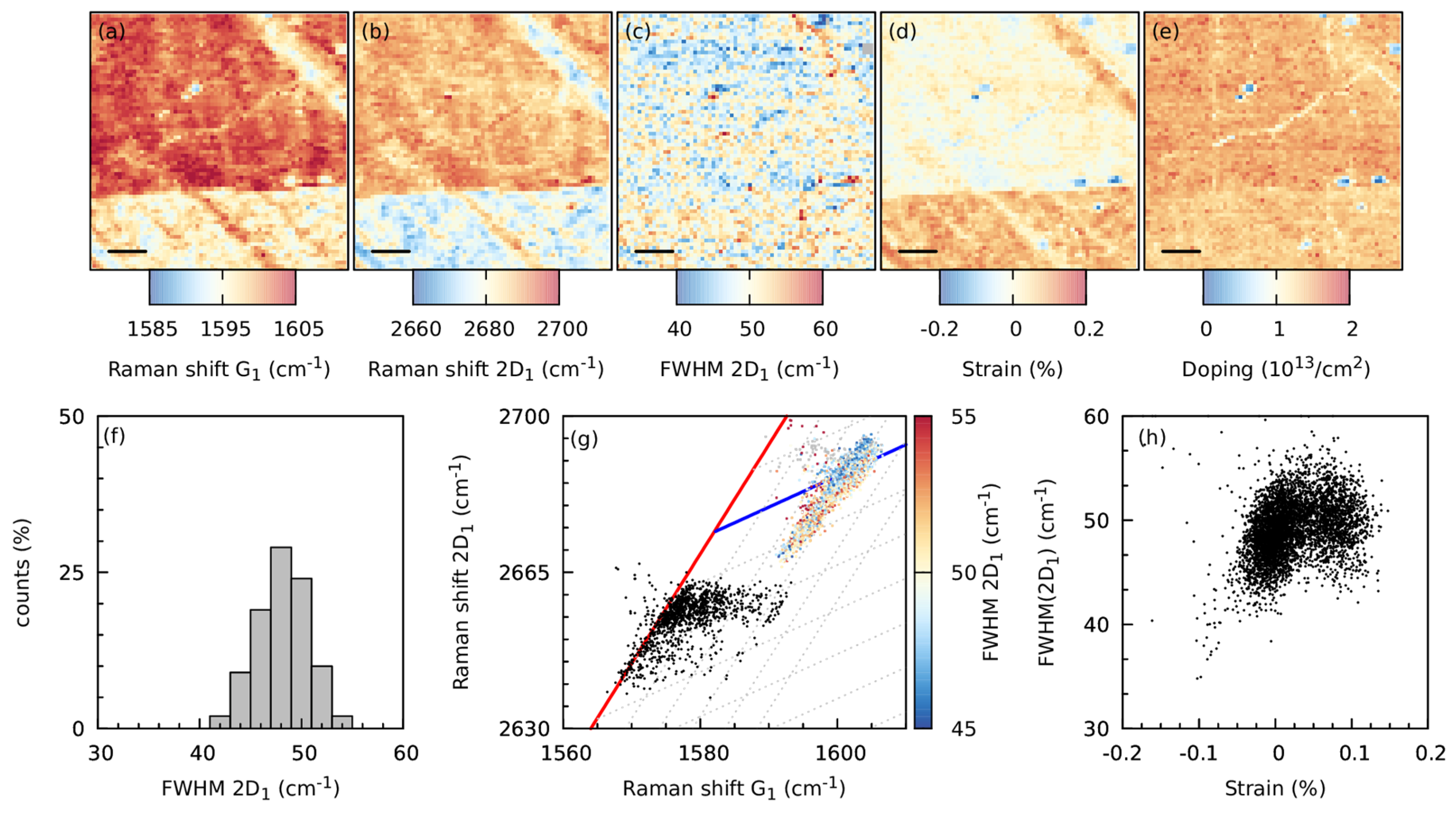
Raman Spectroscopy
4. Discussion
5. Conclusions
Author Contributions
Funding
Conflicts of Interest
References
- Deng, S.; Berry, V. Wrinkled, rippled and crumpled graphene: An overview of formation mechanism, electronic properties, and applications. Mater. Today 2016, 19, 197. [Google Scholar] [CrossRef]
- Zhao, G.; Li, X.; Huang, M.; Zhen, Z.; Zhong, Y.; Chen, Q.; Zhao, X.; He, Y.; Hu, R.; Yang, T.; et al. The physics and chemistry of graphene-on-surfaces. Chem. Soc. Rev. 2017, 46, 4417. [Google Scholar] [CrossRef] [PubMed]
- Chen, M.; Haddon, R.C.; Yana, R.; Bekyarova, E. Advances in transferring chemical vapour deposition graphene: A review. Mater. Horiz. 2017, 4, 1054. [Google Scholar] [CrossRef]
- Wang, L.; Meric, I.; Huang, P.Y.; Gao, Q.; Gao, Y.; Tran, H.; Taniguchi, T.; Watanabe, K.; Campos, L.M.; Muller, D.A.; et al. One-dimensional electrical contact to a two-dimensional material. Science 2013, 342, 614. [Google Scholar] [CrossRef] [PubMed]
- Banszerus, L.; Schmitz, M.; Engels, S.; Dauber, J.; Oellers, M.; Haupt, F.; Watanabe, K.; Taniguchi, T.; Beschoten, B.; Stampfer, C. Ultrahigh-mobility graphene devices from chemical vapor deposition on reusable copper. Sci. Adv. 2015, 1, e1500222. [Google Scholar] [CrossRef] [PubMed]
- Park, S.; Srivastava, D.; Cho, K. Generalized, Chemical reactivity of curved Surfaces: Carbon nanotubes. Nano. Lett. 2003, 3, 1273. [Google Scholar] [CrossRef]
- Haddon, R.C. π-Electrons in three dimensions. Acc. Chem. Res. 1988, 21, 243. [Google Scholar] [CrossRef]
- Niyogi, S.; Hamon, M.A.; Hu, H.; Zhao, B.; Bhowmik, P.; Sen, R.; Itkis, M.E.; Haddon, R.C. Chemistry of Single-Walled Carbon Nanotubes. Acc. Chem. Res. 2002, 35, 1105. [Google Scholar] [CrossRef] [PubMed]
- Wang, Q.H.; Jin, Z.; Kim, K.K.; Hilmer, A.J.; Paulus, G.L.; Shih, C.C.-J.; Ham, M.-H.; Sanchez-Yamagishi, J.D.; Watanabe, K.; Taniguchi, T.; et al. Understanding and controlling the substrate effect on graphene electron-transfer chemistry via reactivity imprint lithography. Nat. Chem. 2012, 7, 724. [Google Scholar] [CrossRef] [PubMed]
- Levy, N.; Burke, S.A.; Meaker, K.L.; Panlasigui, M.; Zettl, A.; Guinea, F.; Castro Neto, A.H.; Crommie, M.F. Strain-induced pseudo magnetic fields greater than 300 tesla in graphene nanobubbles. Science 2010, 329, 544. [Google Scholar] [CrossRef] [PubMed]
- Zhu, W.; Low, T.; Perebeinos, V.; Bol, A.A.; Zhu, Y.; Yan, H.; Tersoff, J.; Avouris, P. Structure and electronic transport in graphene wrinkles. Nano Lett. 2012, 12, 3431. [Google Scholar] [CrossRef] [PubMed]
- Khestanova, E.; Guinea, F.; Fumagalli, L.; Geim, A.K.; Grigorieva, I.V. Universal shape and pressure inside bubbles appearing in van der Waals heterostructures. Nat. Commun. 2016, 7, 2587. [Google Scholar] [CrossRef] [PubMed]
- Vasu, K.S.; Prestat, E.; Abraham, J.; Dix, J.; Kashtiban, R.J.; Beheshtian, J.; Sloan, J.; Carbone, P.; Neek-Amal, M.; Haigh, S.J.; et al. Van der Waals pressure and its effect on trapped interlayer molecules. Nat. Commun. 2016, 7, 12168. [Google Scholar] [CrossRef] [PubMed]
- Algara-Siller, G.; Lehtinen, O.; Wang, F.C.; Nair, R.R.; Kaiser, U.; Wu, H.A.; Geim, A.K.; Grigorieva, I.V. Square ice in graphene nanocapillaries. Nature 2015, 519, 443. [Google Scholar] [CrossRef] [PubMed]
- Hallam, T.; Berner, N.C.; Yim, C.; Duesberg, G.S. Strain, bubbles, dirt, and folds: A study of graphene polymer-assisted transfer. Adv. Mater. Interfaces 2014, 1, 1400115. [Google Scholar] [CrossRef]
- Diab, M.; Kim, K.-S. Ruga-formation instabilities of a graded stiffness boundary layer in a neo-Hookean solid. Proc. R. Soc. A 2014, 470, 20140218. [Google Scholar] [CrossRef]
- Wang, Q.; Zhao, X. A three-dimensional phase diagram of growth-induced surface instabilities. Sci. Rep. 2015, 5, 8887. [Google Scholar] [CrossRef] [PubMed]
- Kalbac, M.; Frank, O.; Kavan, L. Effects of heat treatment on raman spectra of two-layer 12C/13C grapheme. Chem. Eur. J. 2012, 18, 13877. [Google Scholar] [CrossRef] [PubMed]
- Vejpravova, J.; Pacakova, B.; Endres, J.; Mantlikova, A.; Verhagen, T.; Vales, V.; Frank, O.; Kalbac, M. Graphene wrinkling induced by monodisperse nanoparticles: Facile control and quantification. Sci. Rep. 2015, 5, 15061. [Google Scholar] [CrossRef] [PubMed]
- Necas, D.; Klapetek, P. Gwyddion: An open-source software for SPM data analysis. Cent. Eur. J. Phys. 2012, 10, 181. [Google Scholar] [CrossRef]
- Frank, O.; Vejpravova, J.; Holy, V.; Kavan, L.; Kalbac, M. Interaction between graphene and copper substrate: The role of lattice orientation. Carbon 2014, 68, 440. [Google Scholar] [CrossRef]
- Verhagen, T.G.A.; Drogowska, K.; Kalbac, M.; Vejpravova, J. Temperature-induced strain and doping in monolayer and bilayer isotopically labeled graphene. Phys. Rev. B 2015, 92, 125437. [Google Scholar] [CrossRef]
- Lee, J.E.; Ahn, G.; Shim, J.; Lee, Y.S.; Ryu, S. Optical separation of mechanical strain from charge doping in grapheme. Nat. Commun. 2012, 3, 1024. [Google Scholar] [CrossRef] [PubMed]
- Neumann, C.; Reichardt, S.; Venezuela, P.; Drogeler, M.; Banszerus, L.; Schmitz, M.; Watanabe, K.; Taniguchi, T.; Mauri, F.; Beschoten, B.; et al. Raman spectroscopy as probe of nanometre-scale strain variations in grapheme. Nat. Commun. 2015, 6, 8429. [Google Scholar] [CrossRef] [PubMed]
- Frank, O.; Mohr, M.; Maultzsch, J.; Thomsen, C.; Riaz, I.; Jalil, R.; Novoselov, K.S.; Tsoukleri, G.; Parthenios, J.; Papagelis, K.; et al. Raman 2D-Band Splitting in Graphene: Theory and Experiment. ACS Nano 2011, 5, 2231. [Google Scholar] [CrossRef] [PubMed]


| Ra (nm) | Rq (nm) | Rtm (nm) | SA (%) | Awr (%) | wwr (nm) |
|---|---|---|---|---|---|
| 0.83 | 1.03 | 2.5 | 105 | 65 | 6–15 |
© 2019 by the authors. Licensee MDPI, Basel, Switzerland. This article is an open access article distributed under the terms and conditions of the Creative Commons Attribution (CC BY) license (http://creativecommons.org/licenses/by/4.0/).
Share and Cite
Verhagen, T.; Pacakova, B.; Kalbac, M.; Vejpravova, J. Introducing Well-Defined Nanowrinkles in CVD Grown Graphene. Nanomaterials 2019, 9, 353. https://doi.org/10.3390/nano9030353
Verhagen T, Pacakova B, Kalbac M, Vejpravova J. Introducing Well-Defined Nanowrinkles in CVD Grown Graphene. Nanomaterials. 2019; 9(3):353. https://doi.org/10.3390/nano9030353
Chicago/Turabian StyleVerhagen, Tim, Barbara Pacakova, Martin Kalbac, and Jana Vejpravova. 2019. "Introducing Well-Defined Nanowrinkles in CVD Grown Graphene" Nanomaterials 9, no. 3: 353. https://doi.org/10.3390/nano9030353
APA StyleVerhagen, T., Pacakova, B., Kalbac, M., & Vejpravova, J. (2019). Introducing Well-Defined Nanowrinkles in CVD Grown Graphene. Nanomaterials, 9(3), 353. https://doi.org/10.3390/nano9030353