Article

Long Low-Loss-Litium Niobate on Insulator Waveguides with Sub-Nanometer Surface Roughness

1
State Key Laboratory of High Field Laser Physics, Shanghai Institute of Optics and Fine Mechanics, Chinese Academy of Sciences, Shanghai 201800, China
2
University of Chinese Academy of Sciences, Beijing 100049, China
3
State Key Laboratory of Precision Spectroscopy, East China Normal University, Shanghai 200062, China
4
XXL—The Extreme Optoelectromechanics Laboratory, School of Physics and Materials Science, East China Normal University, Shanghai 200241, China
5
Collaborative Innovation Center of Extreme Optics, Shanxi University, Taiyuan 030006, Shanxi, China
*
Author to whom correspondence should be addressed.
These authors contributed equally to this paper.
Nanomaterials 2018, 8(11), 910; https://doi.org/10.3390/nano8110910
Submission received: 5 October 2018 / Revised: 27 October 2018 / Accepted: 2 November 2018 / Published: 6 November 2018
(This article belongs to the Special Issue Synthesis and Modification of Nanostructured Thin Films)

Abstract

:
In this paper, we develop a technique for realizing multi-centimeter-long lithium niobate on insulator (LNOI) waveguides with a propagation loss as low as 0.027 dB/cm. Our technique relies on patterning a chromium thin film coated on the top surface of LNOI into a hard mask with a femtosecond laser followed by chemo-mechanical polishing for structuring the LNOI into the waveguides. The surface roughness on the waveguides was determined with an atomic force microscope to be 0.452 nm. The approach is compatible with other surface patterning technologies, such as optical and electron beam lithographies or laser direct writing, enabling high-throughput manufacturing of large-scale LNOI-based photonic integrated circuits.

1. Introduction

Photonic integrated circuits (PICs) have shown the potential for use in complex information processing systems employing both quantum and classical light sources [1,2]. To increase computational efficiency and reconfigurability, PIC-based optical computers/calculators must have low propagation loss, fast tunability, and efficient optical interfacing. Currently, several materials have been utilized to construct large-scale PICs, including silicon and some semiconductor materials [3,4,5,6], fused silica [7,8], and bulk lithium niobate (LN) [9,10]. The advantage of silicon-based PICs is the high refractive index of silicon that enables the fabrication of compact light circuits with strong confinement and tight bends. In addition, the lithographic technology for high precision patterning of silicon and semiconductors is mature. However, silicon-based PICs intrinsically suffer from a relatively high propagation loss and a transmission window prohibitive for visible and shorter wavelengths. PICs can be built on fused silica and bulk LN crystals by local modification of the refractive index via either illumination of light or ion doping. Unfortunately, the refractive index increases achieved using these approaches are usually in the order of 10−3 to 10−2, resulting in large PICs footprints being required for minimizing the bending loss. Most importantly, the typical propagation losses of waveguides in state-of-the-art PICs are typically in the order of 10−1 dB/cm or higher, which ultimately limits the performance of PIC-based optical computers.
A revolutionary approach for building high-performance PICs has been emerging, enabled by the successful application of high quality lithium niobate on insulator (LNOI) nanophotonic structures. The first experimental proof of this approach was provided by first patterning the LNOI into the designated geometries using a femtosecond laser. The draft structures obtained after the femtosecond laser patterning, which has a relatively high sidewall roughness in the order of tens of nanometers, were then polished with a focused ion beam (FIB) milling to smoothen the sidewall [11]. This concept was soon incorporated into other lithographic technologies, such as optical lithography and electron beam writing (EBW), for defining the planar patterns on LNOI substrates followed by reactive ion etching to complete the nanostructuring of the LNOI [12,13]. The initial focus was mainly on optical microresonators [11,12,13,14,15,16,17,18,19,20,21], and other devices (such as waveguides and photonic crystals [22,23,24,25,26,27,28]) appeared shortly, taking advantage of the high surface smoothness of the sidewalls as a result of the ion dry etching. So far, the propagation loss in the LNOI waveguides has reached 0.04 dB/cm, highlighting their potential for use in large-scale PIC applications [29].
Notably, the ion etching step, which is necessary for achieving high quality sidewalls on LNOI nanophotonic structures, leaves a low but non-negligible surface roughness that is difficult to completely remove [29]. Moreover, the use of FIB or EBW in the patterning of LNOI makes the approach impractical for fabricating large-scale PICs due to their low throughputs and limited range of motion. Recently, we developed a technique for fabricating high-quality optical microresonators on LNOI with a quality factor above 107 [30]. Since this technique does not involve an ion beam etching process, surface smoothness beyond that allowed by ion beam etching can be readily achieved, and the footprint sizes of PICs can be increased by patterning the LNOI photonic structures with either laser direct writing or optical lithography. Here, we experimentally show that we are able to realize 10-cm-long LNOI waveguides with a propagation loss of 0.027 dB/cm, which benefited from the low surface roughness of 0.452 nm measured with an atomic force microscope (AFM). The low loss waveguides can be essential building blocks for light modulation, beam delivery and manipulation, nonlinear optics, and optical signal processing.

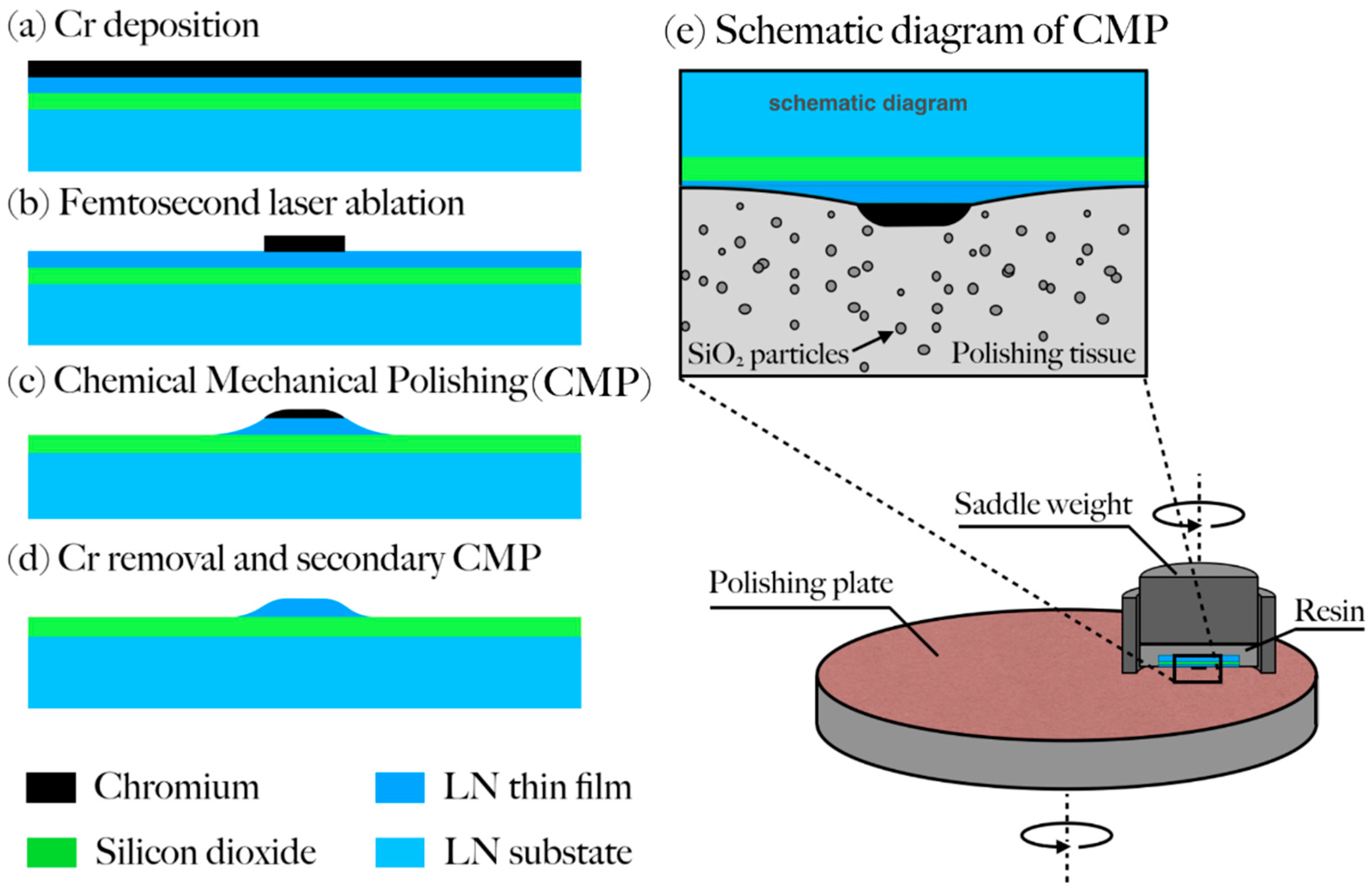
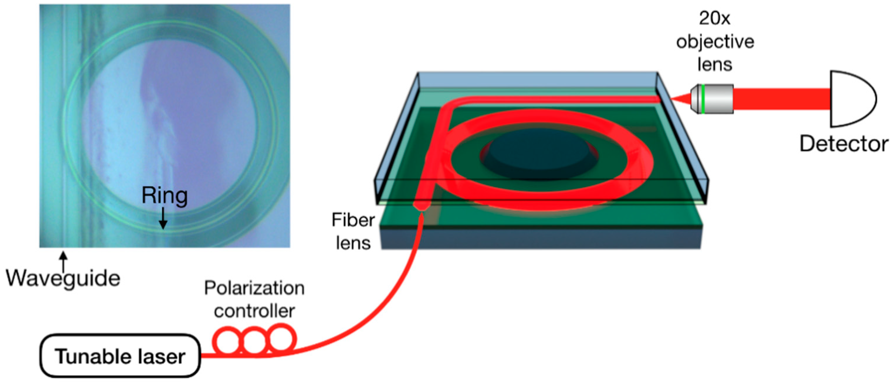
2. Materials and Methods
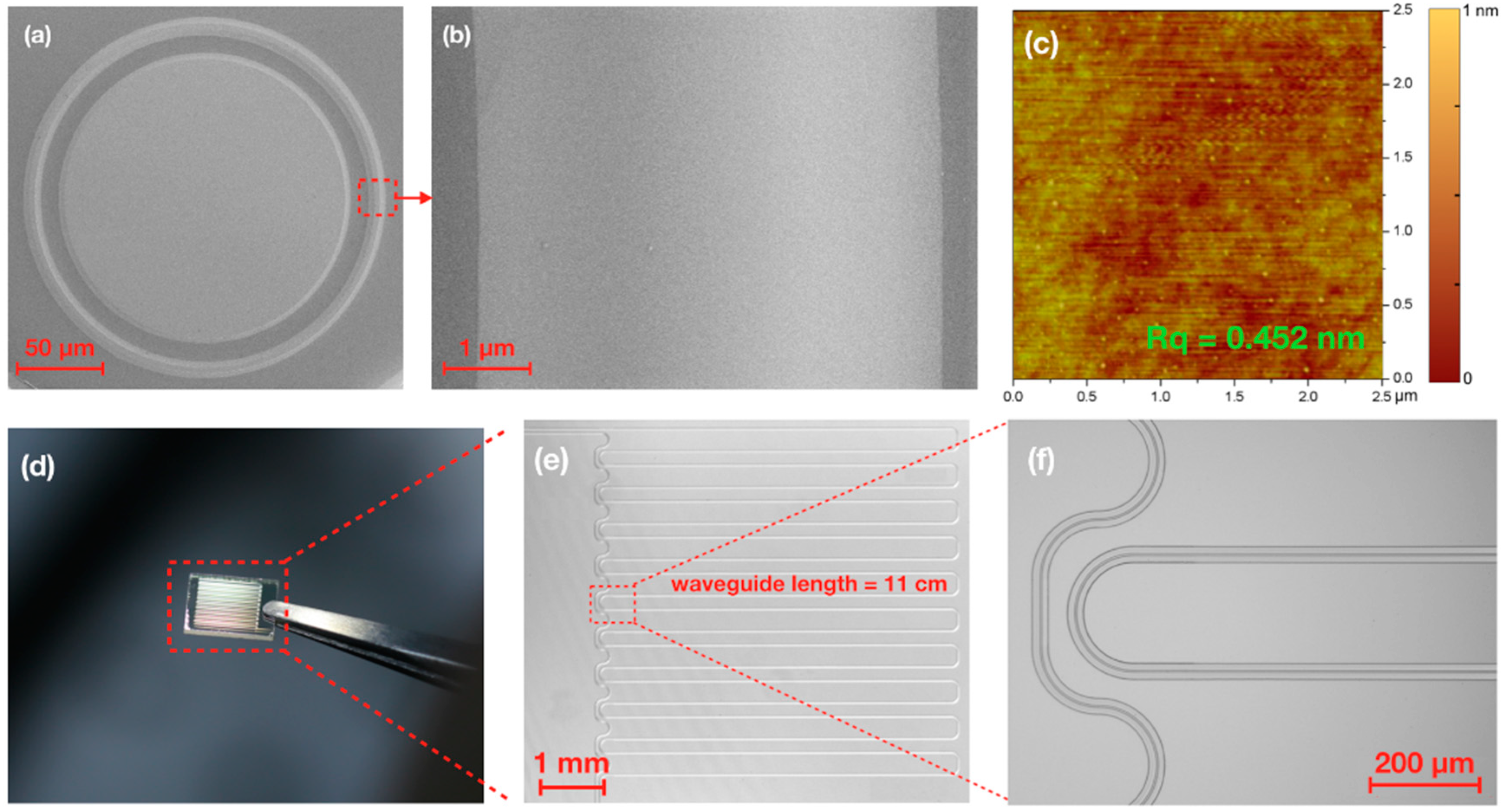
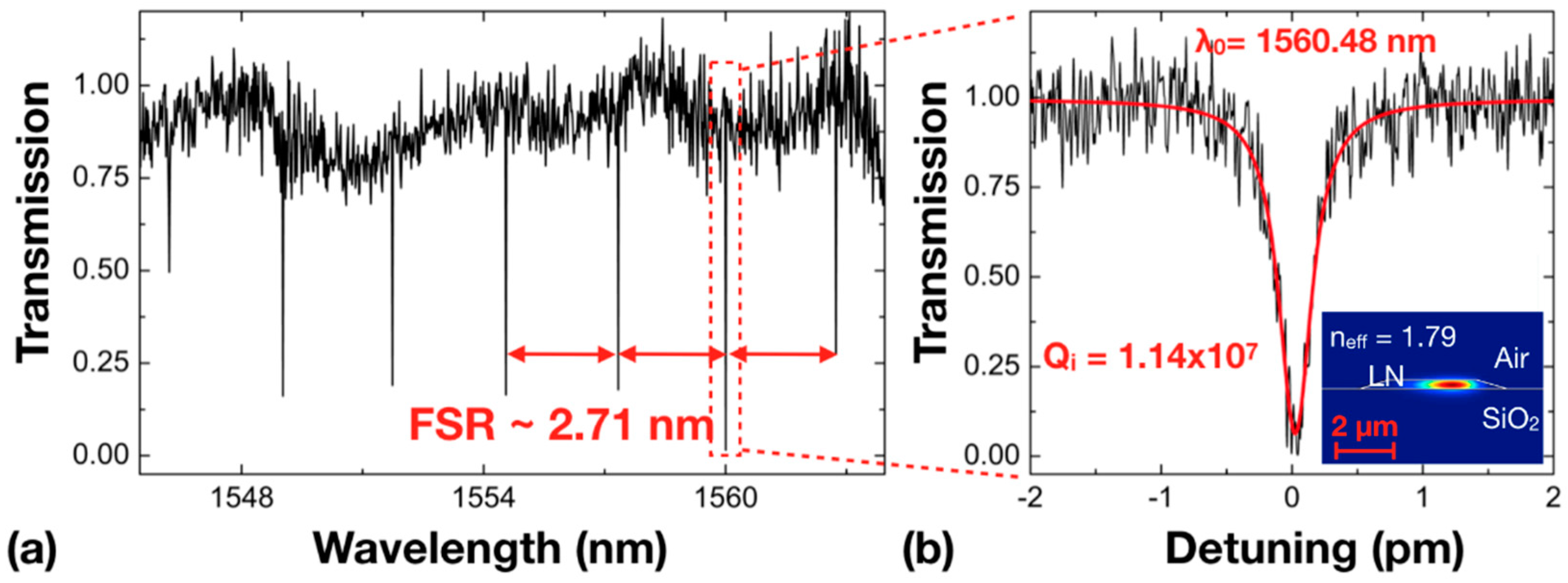
A commercially available X-cut LNOI wafer fabricated by ion slicing (NANOLN, Jinan Jingzheng Electronics Co., Ltd., Jinan, Shandong, China) was chosen in our experiment as the material upon which the LNOI waveguides were produced [31]. The LN thin film had a thickness of 400 nm and was bonded to a SiO2 layer 2-μm-thick, which was grown on a LN substrate. The fabrication procedures are schematically illustrated in Figure 1, including (1) deposition of a thin layer of chromium (Cr) with a thickness of 600 nm on LNOI by magnetron sputtering and (2) patterning of the Cr film using femtosecond laser ablation. It is critical to carefully choose the pulse energy of the femtosecond laser to ensure the complete removal of the Cr film without damaging the LNOI underneath, which is enabled by the unique characteristics of the interaction of femtosecond laser pulses with various types of materials [32]. More details on the laser parameters can be found in Wu, R., et al. [30]. To produce a tightly focused spot ~1 μm in diameter, a 100× objective lens (M Plan Apo NIR, Mitutoyo Corporation, Kawasaki, Kanagawa, Japan) with a numerical aperture (NA) of 0.7 was used in our experiment. Femtosecond laser direct writing was conducted by translating the LNOI sample with a computer-controlled XY motion stage (ABL15020WB and ABL15020, Aerotech Inc., Pittsburgh, PA, USA, translation resolution ~100 nm). The focus of the laser beam was controlled in the Z direction using another one-dimensional stage with a translation resolution of 100 nm (ANT130-110-L-ZS, Aerotech Inc., Pittsburgh, PA, USA) on which the objective lens was installed. A charged coupled device (CCD) was installed above the objective lens for monitoring the fabrication process. The laser power was chosen to ensure the complete removal of the Cr thin film while keeping the LNOI underneath the Cr film intact. The patterned Cr disk served as a hard mask in the subsequent CM polishing.
The CM polishing was carried out using a wafer polishing machine (NUIPOL802, Hefei Kejing Materials Technology Co., Ltd., Hefei, Anhui, China). More details on CM polishing can also be found in Wu, R, et al. [30]. Note that the Cr film has a higher hardness than the LNOI, so LNOI would be completely removed by CM polishing, unless it is protected by a Cr mask. Finally, the Cr mask was removed by immersing the fabricated sample in a Cr etching solution (Chromium etchant, Alfa Aesar GmbH, Haverhill, MA, USA) for 10 min. All the procedures up to this stage were the same as those used for fabricating a high-Q microresonator, as described by Wu, R., et al. [30], For fabricating low-loss waveguides, the sample underwent an additional CM polishing at a relatively low pressure with a shorter polishing duration to improve the smoothness of the upper surface of LN waveguide, as illustrated in Figure 1d.
To characterize the propagation loss in the LNOI waveguide, we constructed a whispering gallery ring resonator through which the propagation loss of the LNOI waveguide was determined using α = 2πneff/(), where α is the attenuation coefficient, neff the effective refractive index, Q the quality factor of the ring resonator, and λ is the wavelength of the light beam. Both neff and the Q-factor were determined from the transmission spectrum of microring resonator. The experimental setup for measuring the Q factor of the ring resonator is schematically shown in Figure 2. The light produced by a tunable laser (LTB-6728, Newport Corporation, Santa Clara, CA, USA) was coupled to a curved LNOI waveguide whose geometric parameters, including the thickness and width, were the same as that of the LNOI ring, determined with the use of a fiber lens. The exiting light was collected using a 20× objective lens (MPlanFL N, Olympus Corporation, Tokyo, Japan) into a detector (Model 1811, Newport Corporation, Santa Clara, CA, USA). The bend of the upper waveguide was intentionally introduced for preventing the stray light from the fiber laser from entering the objective lens located in front of the detector. The polarization direction of the light was adjusted with a fiber polarization controller. The curved waveguide was coupled to the LNOI ring resonator via evanescent coupling. Specifically, by carefully adjusting the distance between the coupling waveguide and the microring resonator, we were able to achieve the coupling condition crucial for obtaining an accurate intrinsic Q factor of the ring resonator. We fabricated five microrings and the measured optical losses were close to each other (with Q factors between 106 and 107), indicating that the fabrication technique is reliable and reproducible.

3. Results

Figure 3a shows the top-view scanning electron microscope (SEM) images of a LN micro ring resonator with a diameter of 160 μm. The width of the waveguide was ~3 μm. The close-up-view SEM of an arc of the ring highlights the high surface smoothness of the CM polished sample. A further atomic force microscope (AFM) inspection, as illustrated in Figure 3c, confirmed that a surface roughness Rq as low as 0.452 nm was achieved. The same fabrication technique was also used to fabricate a continuous 11-cm-long optical waveguide, as shown by the digital-camera-captured picture in Figure 3d, with details provided in the zoomed optical micrographs in Figure 3e–f. The total time of femtosecond laser ablation for fabricating the 11-cm-long waveguide was 90 min. At this moment, the footprint size of the PICs was only limited by the LNOI wafer size. The LNOI wafer can be made larger without much difficulty [33].
The optical loss characterization was performed using whispering-gallery-resonator-loss measurements. The propagation loss α is related to the Q factor of the ring resonator. Figure 4a shows the measured transmission spectrum for the wavelength range between 1546 and 1564 nm. The free spectral range (FSR) of the microring resonator was determined to be 2.71 nm, which is consistent with the 160 μm diameter of our ring resonator. The resonant lines appeared regularly spaced, indicating that mostly low-order modes exist in the ring resonator. One of the whispering-gallery modes at the resonant wavelength of 1560.48 nm was chosen for the measurement of the loaded Q factor by fitting with a Lorentz function, which reached 5.70 × 10⁶, corresponding to an intrinsic Q factor of 1.14 × 10⁷ in the critical coupling regime as evidenced in Figure 4b. The effective refractive index, neff = λ2/(2πR·FSR), with a ring radius R of 80 μm and wavelength of 1560.48 nm, was calculated to be 1.79, which is in good agreement with our finite-difference time-domain (FDTD) simulation result given in the inset of Figure 4b. Combining the effective refractive index and the Q- factor obtained from the transmission spectrum, the propagation loss in the microring resonator was calculated to be 0.027 dB/cm using the aforementioned expression α = 2πneff/(). This result represents the upper limit of the propagation loss in the LNOI waveguide fabricated using our method.

4. Discussion

The low propagation loss of 0.027 dB/cm was a result of the low surface roughness Rq of 0.452 nm on the fabricated LNOI waveguides. The surface roughness was improved using our technique in which the LNOI is purely patterned by the chemo-mechanical polishing without any use of ion beam etching [30]. The ion beam etching inherently leaves a small amount of surface roughness on the nearly vertical sidewalls, which is difficult to completely remove by top surface polishing [34,35]. This is the major reason that we were able to obtain a propagation loss lower than the waveguides fabricated by FIB or reactive ion etching. In the current experiment, we used a femtosecond laser to pattern the Cr hard mask. Generally speaking, the sidewall roughness on the Cr mask patterned by femtosecond laser ablation should be higher than the surface roughness of the LNOI photonic structures produced by ion beam etching. However, the sidewall roughness on the Cr mask only transfers to the underneath LNOI near the top surface, thus it can be completely suppressed with an additional polishing process for thinning the LNOI substrate after the removal of the Cr mask (Figure 1d).
Notably, the propagation loss obtained by measuring the Q factor of the ring resonator may have been underestimated for the straight segments in the LNOI waveguides, as presented in Figure 3d–f, due to a higher radiative loss in the ring resonator. Ultimately, the propagation loss of the LNOI waveguides is limited by the absorption in crystalline LN, which is well known to be in the order of ~10−3 dB/cm. Our measured loss was still one order of magnitude away from the theoretical limit, which could be attributed to several factors, including the radiative loss in the ring resonator and some unknown contamination on the surface of the LNOI waveguide, as the measurements were all carried out in a low-class clean room, existence of absorptive defects in the LNOI substrate owing to the imperfect crystal growth, and the remaining surface roughness left by the chemo-mechanical polishing process. Thus, to realize LNOI waveguides with propagation losses in the order of 1 × 10⁻³ dB/cm, many refinements should be systematically investigated in the future.
The fabrication resolution of femtosecond laser direct writing is typically in the order of 1 μm for inorganic materials such as glass, semiconductors, and metals. However, today’s optical lithography can easily achieve sub-micron or even 100-nm-level patterning resolutions. This should be sufficient for fabricating single-mode LNOI waveguides of narrower widths by which PICs, such as Mach-Zender interferometers and polarization convertors, can be built. The mode field of the LNOI waveguides can be tuned by coating them with fused silica for suppressing higher order modes as well as scattering loss due to the reduced contrast of the refractive index between the LNOI waveguide and the cladding environment [36]. With these improvements, the LNOI waveguides will become a major building block for PIC applications.

5. Conclusions

In this study, we achieved a propagation loss of 0.027 dB/cm in LNOI waveguides fabricated by combining femtosecond laser micromachining for patterning the Cr mask and chemo-mechanical polishing for transferring the laser-written patterns to the LNOI beneath the Cr mask. By eliminating the low-throughput FIB or EBW process, our technique enables the rapid fabrication of longer low-loss optical waveguides, which are only limited by the range of motion of the air bearing stage and the size of the LNOI wafers. Thus, our approach promotes the fabrication efficiency and reduces the cost of manufacturing LNOI PICs. The waveguides and ring resonators can be adopted for constructing complex PICs, enabling the mass production of LNOI PICs for optical communication and computation applications.

Author Contributions

Conceptualization, Y.C.; methodology, Y.C.; software, R.W.; validation, R.W. and M.W.; formal analysis, R.W.; investigation, R.W., M.W., J.Q. and J.X.; resources, R.W., M.W., W.C., Z.F., J.Z. (Jianhao Zhang), J.Z. (Junxia Zhou), L.Q., Z.C. and J.L.; data curation, R.W. and M.W.; writing—original draft preparation, Y.C. and R.W.; writing—review and editing, Y.C., R.W., M.W., J.L. and J.X.; visualization, R.W., J.Q., J.X. and M.W.; supervision, Y.C.; project administration, L.Q. and Z.C.; funding acquisition, Y.C., J.L. and J.X.

Funding

This research was funded by the National Natural Science Foundation of China (Grant Nos. 11734009, 11874375, 61590934, 61635009, 61327902, 61505231, 11604351, 11674340, 61575211, 61675220, 61761136006), the Strategic Priority Research Program of Chinese Academy of Sciences (Grant No. XDB16000000), the Key Research Program of Frontier Sciences, Chinese Academy of Sciences (Grant No. QYZDJ-SSW-SLH010), the Project of Shanghai Committee of Science and Technology (Grant No. 17JC1400400), the Shanghai Rising-Star Program (Grant No. 17QA1404600), and the Shanghai Pujiang Program (Grant No.18PJ1403300).

Conflicts of Interest

The authors declare no conflict of interest.

References

  1. Ladd, T.D.; Jelezko, F.; Laflamme, R.; Nakamura, Y.; Monroe, C.; O’Brien, J.L. Quantum computers. Nature 2010, 464, 45–53. [Google Scholar] [CrossRef] [PubMed]
  2. Shen, Y.; Harris, N.C.; Skirlo, S.; Prabhu, M.; Baehr-Jones, T.; Hochberg, M.; Sun, X.; Zhao, S.; Larochelle, H.; Englund, D.; et al. Deep learning with coherent nanophotonic circuits. Nat. Photonics 2017, 11, 441. [Google Scholar] [CrossRef]
  3. Harris Nicholas, C.; Bunandar, D.; Pant, M.; Steinbrecher Greg, R.; Mower, J.; Prabhu, M.; Baehr-Jones, T.; Hochberg, M.; Englund, D. Large-scale quantum photonic circuits in silion. Nacnophotonics 2016, 5, 456–468. [Google Scholar] [CrossRef]
  4. Dietrich, C.P.; Fiore, A.; Thompson, M.G.; Kamp, M.; Höfling, S. GaAs integrated quantum photonics: Towards compact and multi-functional quantum photonic integrated circuits. Laser Photonics Rev. 2016, 10, 870–894. [Google Scholar] [CrossRef] [Green Version]
  5. Najafi, F.; Mower, J.; Harris, N.C.; Bellei, F.; Dane, A.; Lee, C.; Hu, X.; Kharel, P.; Marsili, F.; Assefa, S.; et al. On-chip detection of non-classical light by scalable integration of single-photon detectors. Nat. Commun. 2015, 6, 5873. [Google Scholar] [CrossRef] [PubMed] [Green Version]
  6. Yang, K.Y.; Oh, D.Y.; Lee, S.H.; Yang, Q.-F.; Yi, X.; Shen, B.; Wang, H.; Vahala, K. Bridging ultrahigh-Q devices and photonic circuits. Nat. Photonics 2018, 12, 297–302. [Google Scholar] [CrossRef] [Green Version]
  7. Qiang, X.; Zhou, X.; Wang, J.; Wilkes, C.M.; Loke, T.; O’Gara, S.; Kling, L.; Marshall, G.D.; Santagati, R.; Ralph, T.C.; et al. Large-scale silicon quantum photonics implementing arbitrary two-qubit processing. Nat. Photonics 2018, 12, 534–539. [Google Scholar] [CrossRef]
  8. Marshall, G.D.; Politi, A.; Matthews, J.C.F.; Dekker, P.; Ams, M.; Withford, M.J.; O’Brien, J.L. Laser written waveguide photonic quantum circuits. Opt. Express 2009, 17, 12546–12554. [Google Scholar] [CrossRef] [PubMed]
  9. Sohler, W.; Hu, H.; Ricken, R.; Quiring, V.; Vannahme, C.; Herrmann, H.; Büchter, D.; Reza, S.; Grundkötter, W.; Orlov, S.; et al. Integrated optical devices in lithium niobate. Opt. Photonics News 2008, 19, 24–31. [Google Scholar] [CrossRef]
  10. Jin, H.; Liu, F.M.; Xu, P.; Xia, J.L.; Zhong, M.L.; Yuan, Y.; Zhou, J.W.; Gong, Y.X.; Wang, W.; Zhu, S.N. On-chip generation and manipulation of entangled photons based on reconfigurable lithium-niobate waveguide circuits. Phys. Rev. Lett. 2014, 113, 103601. [Google Scholar] [CrossRef] [PubMed]
  11. Lin, J.; Xu, Y.; Fang, Z.; Song, J.; Wang, N.; Qiao, L.; Fang, W.; Cheng, Y. Second harmonic generation in a high-Q lithium niobate microresonator fabricated by femtosecond laser micromachining. arXiv, 2014; arXiv:1405.6473. [Google Scholar]
  12. Wang, J.; Bo, F.; Wan, S.; Li, W.; Gao, F.; Li, J.; Zhang, G.; Xu, J. High-Q lithium niobate microdisk resonators on a chip for efficient electro-optic modulation. Opt. Express 2015, 23, 23072–23078. [Google Scholar] [CrossRef] [PubMed]
  13. Wang, C.; Burek, M.J.; Lin, Z.; Atikian, H.A.; Venkataraman, V.; Huang, I.-C.; Stark, P.; Lončar, M. Integrated high quality factor lithium niobate microdisk resonators. Opt. Express 2014, 22, 30924–30933. [Google Scholar] [CrossRef] [PubMed]
  14. Lin, J.; Xu, Y.; Fang, Z.; Wang, M.; Song, J.; Wang, N.; Qiao, L.; Fang, W.; Cheng, Y. Fabrication of high-Q lithium niobate microresonators using femtosecond laser micromachining. Sci. Rep. 2015, 5, 8072. [Google Scholar] [CrossRef] [PubMed] [Green Version]
  15. Lin, J.; Xu, Y.; Ni, J.; Wang, M.; Fang, Z.; Qiao, L.; Fang, W.; Cheng, Y. Phase-matched second-harmonic generation in an on-chip LiNbO3 microresonator. Phys. Rev. Appl. 2016, 6, 014002. [Google Scholar] [CrossRef]
  16. Lin, J.; Xu, Y.; Fang, Z.; Wang, M.; Wang, N.; Qiao, L.; Fang, W.; Cheng, Y. Second harmonic generation in a high-Q lithium niobate microresonator fabricated by femtosecond laser micromachining. Sci. China Phys. Mech. Astron. 2015, 58, 114209. [Google Scholar] [CrossRef]
  17. Hao, Z.; Wang, J.; Ma, S.; Mao, W.; Bo, F.; Gao, F.; Zhang, G.; Xu, J. Sum-frequency generation in on-chip lithium niobate microdisk resonators. Photonics Res. 2017, 5, 623–628. [Google Scholar] [CrossRef]
  18. Wang, L.; Wang, C.; Wang, J.; Bo, F.; Zhang, M.; Gong, Q.; Lončar, M.; Xiao, Y.-F. High-Q chaotic lithium niobate microdisk cavity. Opt. Lett. 2018, 43, 2917–2920. [Google Scholar] [CrossRef] [PubMed]
  19. Luo, R.; Jiang, H.; Rogers, S.; Liang, H.; He, Y.; Lin, Q. On-chip second-harmonic generation and broadband parametric down-conversion in a lithium niobate microresonator. Opt. Express 2017, 25, 24531–24539. [Google Scholar] [CrossRef] [PubMed]
  20. Jiang, W.C.; Lin, Q. Chip-scale cavity optomechanics in lithium niobate. Sci. Rep. 2016, 6, 36920. [Google Scholar] [CrossRef] [PubMed] [Green Version]
  21. Fang, Z.; Xu, Y.; Wang, M.; Qiao, L.; Lin, J.; Fang, W.; Cheng, Y. Monolithic integration of a lithium niobate microresonator with a free-standing waveguide using femtosecond laser assisted ion beam writing. Sci. Rep. 2017, 7, 45610. [Google Scholar] [CrossRef] [PubMed] [Green Version]
  22. Liang, H.; Luo, R.; He, Y.; Jiang, H.; Lin, Q. High-quality lithium niobate photonic crystal nanocavities. Optica 2017, 4, 1251–1258. [Google Scholar] [CrossRef]
  23. Wang, C.; Zhang, M.; Stern, B.; Lipson, M.; Lončar, M. Nanophotonic lithium niobate electro-optic modulators. Opt. Express 2018, 26, 1547–1555. [Google Scholar] [CrossRef] [PubMed] [Green Version]
  24. Wang, C.; Xiong, X.; Andrade, N.; Venkataraman, V.; Ren, X.-F.; Guo, G.-C.; Lončar, M. Second harmonic generation in nano-structured thin-film lithium niobate waveguides. Opt. Express 2017, 25, 6963–6973. [Google Scholar] [CrossRef] [PubMed]
  25. Luo, R.; He, Y.; Liang, H.; Li, M.; Lin, Q. Highly tunable efficient second-harmonic generation in a lithium niobate nanophotonic waveguide. Optica 2018, 5, 1006–1011. [Google Scholar] [CrossRef]
  26. Cai, L.; Han, H.; Zhang, S.; Hu, H.; Wang, K. Photonic crystal slab fabricated on the platform of lithium niobate-on-insulator. Opt. Lett. 2014, 39, 2094–2096. [Google Scholar] [CrossRef] [PubMed]
  27. Diziain, S.; Geiss, R.; Steinert, M.; Schmidt, C.; Chang, W.-K.; Fasold, S.; Füßel, D.; Chen, Y.-H.; Pertsch, T. Self-suspended micro-resonators patterned in Z-cut lithium niobate membranes. Opt. Mater. Express 2015, 5, 2081–2089. [Google Scholar] [CrossRef]
  28. Krasnokutska, I.; Tambasco, J.-L.J.; Li, X.; Peruzzo, A. Ultra-low loss photonic circuits in lithium niobate on insulator. Opt. Express 2018, 26, 897–904. [Google Scholar] [CrossRef] [PubMed] [Green Version]
  29. Wolf, R.; Breunig, I.; Zappe, H.; Buse, K. Scattering-loss reduction of ridge waveguides by sidewall polishing. Opt. Express 2018, 26, 19815–19820. [Google Scholar] [CrossRef] [PubMed]
  30. Wu, R.; Zhang, J.; Yao, N.; Fang, W.; Qiao, L.; Chai, Z.; Lin, J.; Cheng, Y. Lithium niobate micro-disk resonators of quality factors above 107. Opt. Lett. 2018, 43, 4116–4119. [Google Scholar] [CrossRef] [PubMed]
  31. Poberaj, G.; Hu, H.; Sohler, W.; Guenter, P. Lithium niobate on insulator (LNOI) for micro-photonic devices. Laser Photonics Rev. 2012, 6, 488–503. [Google Scholar] [CrossRef]
  32. Sugioka, K.; Cheng, Y. Ultrafast lasers—Reliable tools for advanced materials processing. Light Sci. Appl. 2014, 3, e149. [Google Scholar] [CrossRef]
  33. Boes, A.; Corcoran, B.; Chang, L.; Bowers, J.; Mitchell, A. Status and potential of lithium niobate on insulator (LNOI) for photonic integrated circuits. Laser Photonics Rev. 2018, 12, 1700256. [Google Scholar] [CrossRef]
  34. Wolf, R.; Breunig, I.; Zappe, H.; Buse, K. Cascaded second-order optical nonlinearities in on-chip micro rings. Opt. Express 2017, 25, 29927–29933. [Google Scholar] [CrossRef] [PubMed]
  35. Wolf, R.; Breunig, I.; Zappe, H.; Buse, K. Q-factor enhancement of integrated lithium-niobate-on-insulator ridge waveguide whispering-gallery-mode resonators by surface polishing. In Proceedings of the Laser Resonators, Microresonators, and Beam Control XIX, San Francisco, CA, USA, 20 February 2017; p. 1009002. [Google Scholar] [CrossRef]
  36. Guarino1, A.; Poberaj, G.; Rezzonico, D.; Degl’Innocenti, R.; Günter, P. Electro–optically tunable microring resonators in lithium niobate. Nat. Photonics 2007, 1, 407–410. [Google Scholar] [CrossRef] [Green Version]
Figure 1. (ad) Flow-chart of fabrication of lithium niobate on insulator (LNOI) waveguide and (e) schematic diagram of chemo-mechanical polishing (CMP).
Nanomaterials 08 00910 g001
Figure 2. Schematic of the experimental setup for measuring the Q factor of the microring resonator. Left inset: Optical micrograph image of the microring resonator coupling with the waveguide, as indicated by the black arrows.
Nanomaterials 08 00910 g002
Figure 3. (a) Top-view scanning electron microscope (SEM) image of a lithium niobate (LN) microring resonator; (b) Zoomed view of the ridge of the microring resonator in (a); (c) Atomic force microscope (AFM) image of the ridge; (d) Picture of a chip consisting of an 11-cm-long waveguide captured by digital camera; (e,f) Zoomed images of the waveguides on the chip captured with an optical microscope.
Nanomaterials 08 00910 g003
Figure 4. (a) Transmission spectrum of the LN microring resonator; (b) The Lorentz fitting (red curve) reveals a loaded Q factor of 5.70 × 10⁶, corresponding to an intrinsic Q factor of 1.14 × 10⁷. Inset: The optical mode distribution and neff in the ring waveguide calculated using finite-difference time-domain (FDTD) simulation.
Nanomaterials 08 00910 g004

