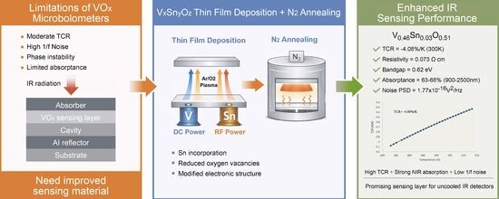
Effect of Annealing on Electrical and Optical Properties of Tin-Doped Vanadium Oxide Films for Microbolometer Applications


Abstract
1. Introduction
2. Experimental Details
2.1. Film Deposition
2.2. Annealing
2.3. Atomic Compositions
2.4. Thickness and Surface Morphology
2.5. X-Ray Diffraction (XRD)
2.6. Transmission, Reflection, Absorption and Optical Bandgap
2.7. Resistivity and TCR Measurement
2.8. Optical Constants
2.9. Noise Measurement
3. Results
3.1. Atomic Composition
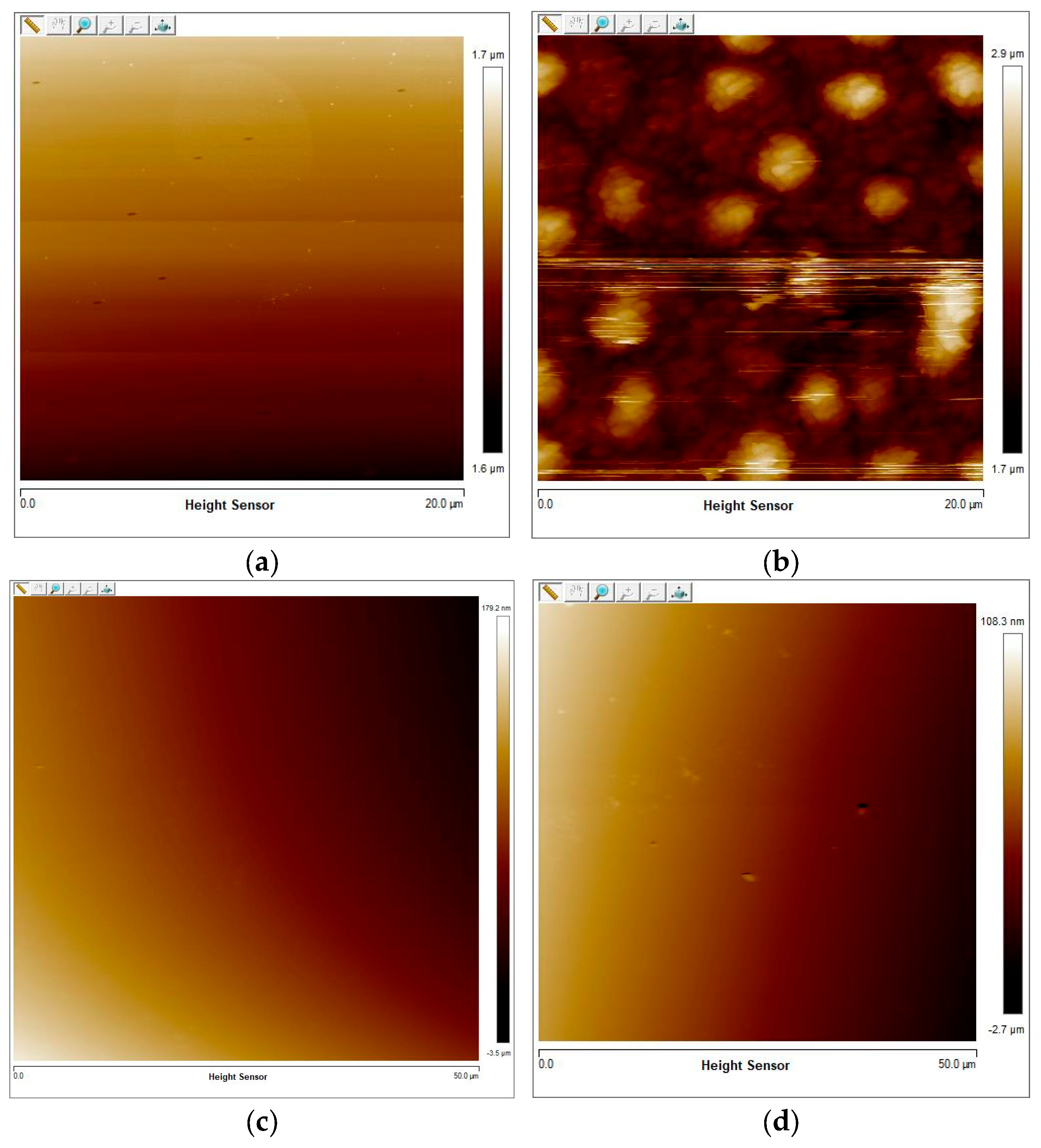
3.2. Thickness and Surface Morphology
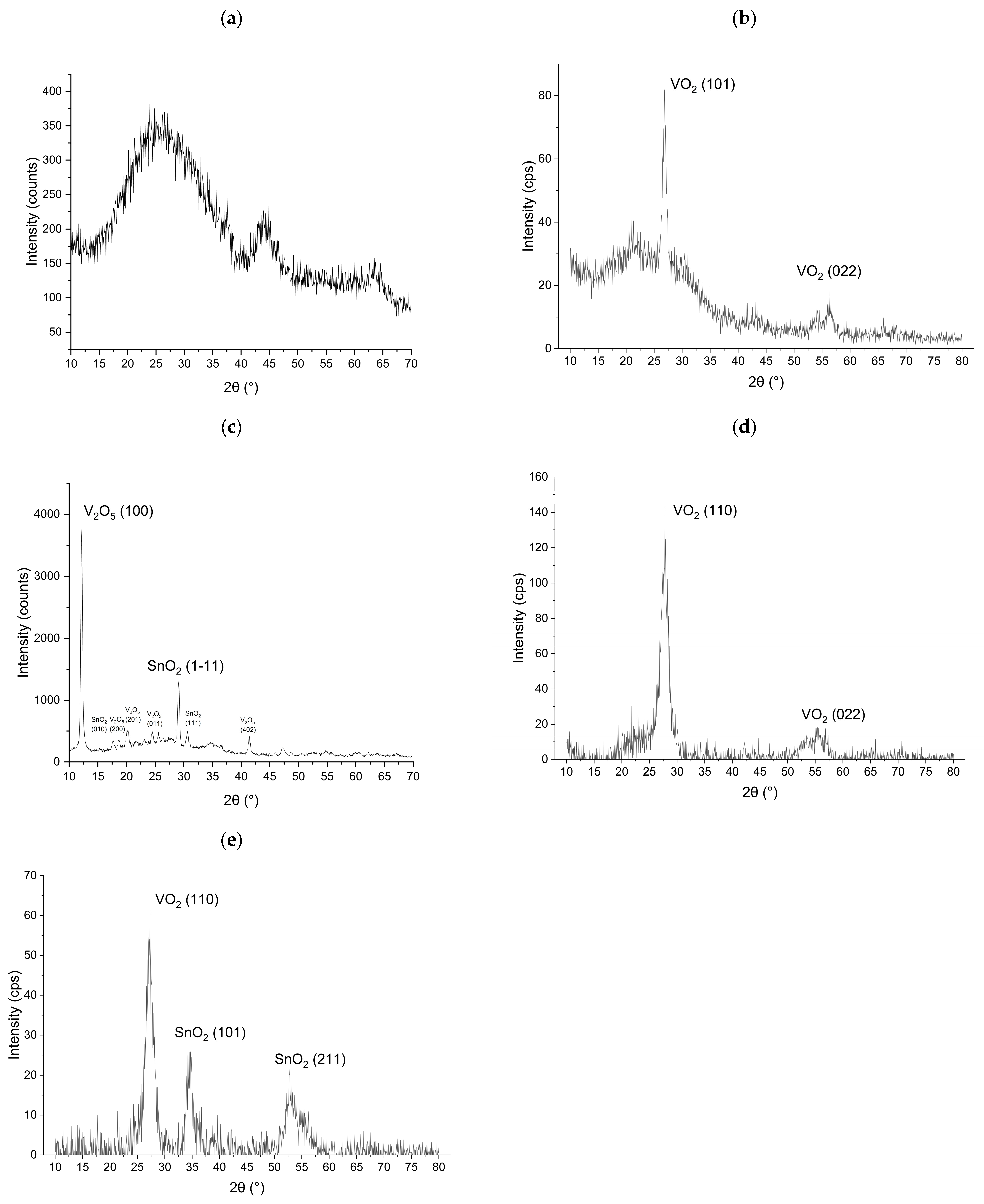
3.3. XRD Measurement
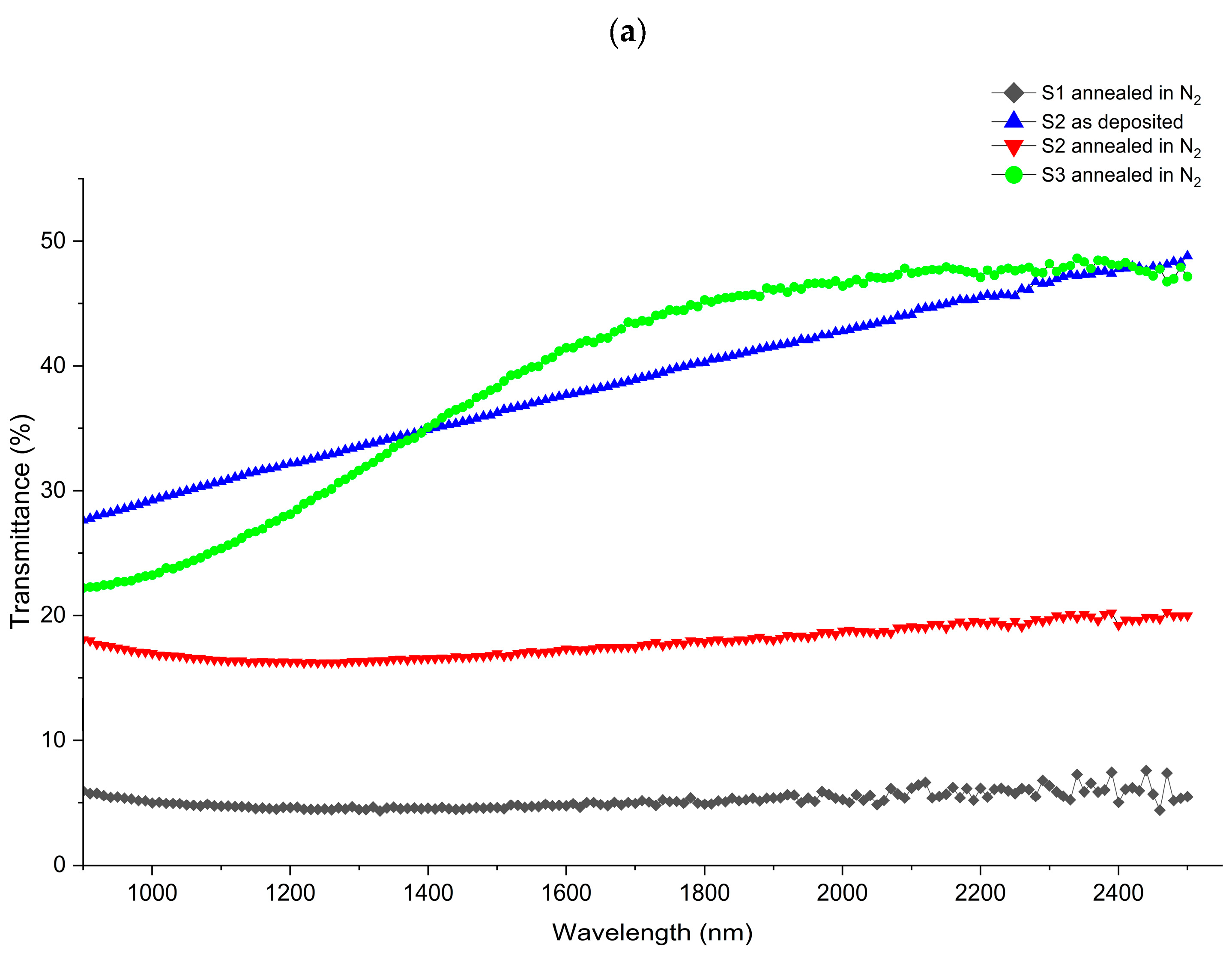
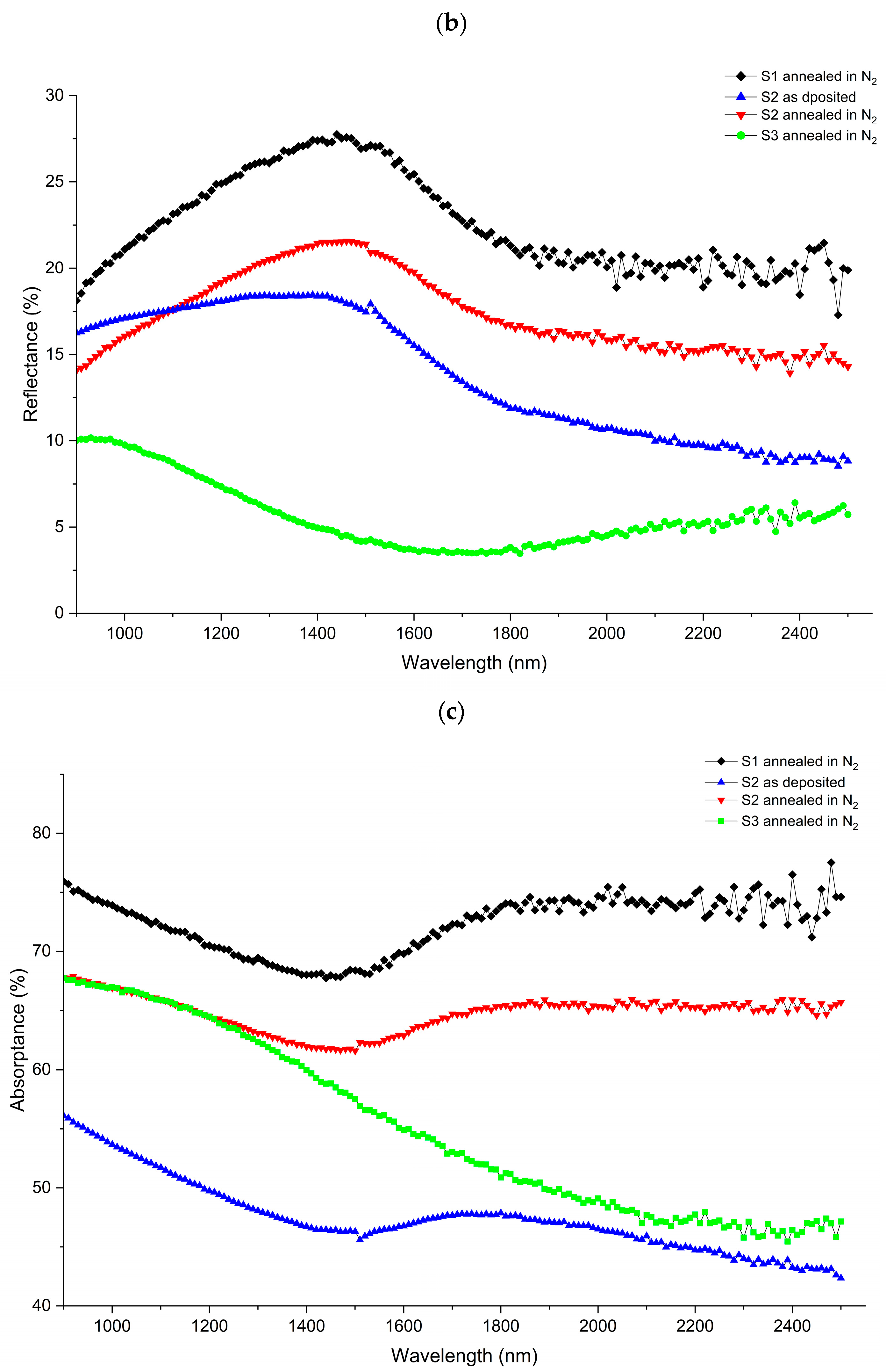
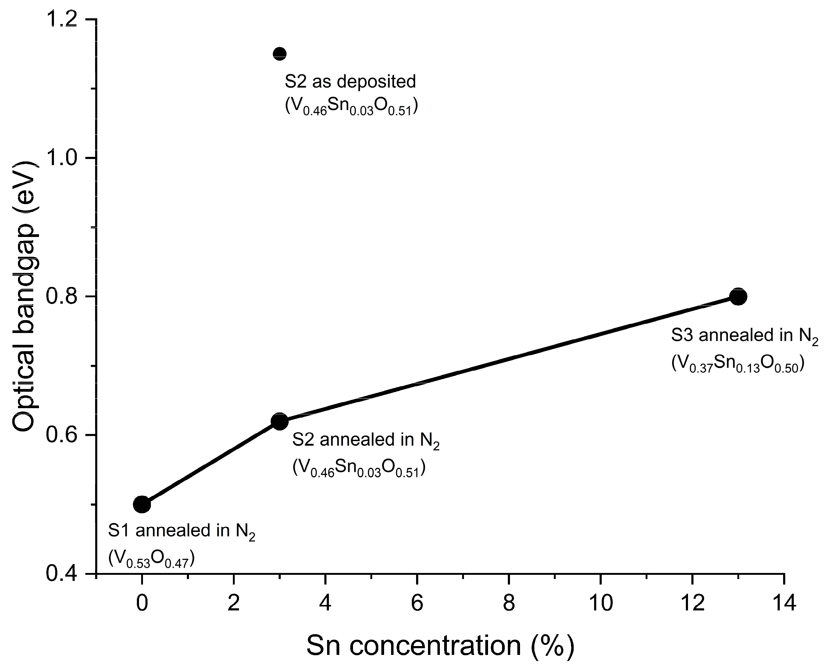
3.4. Absorption and Bandgap
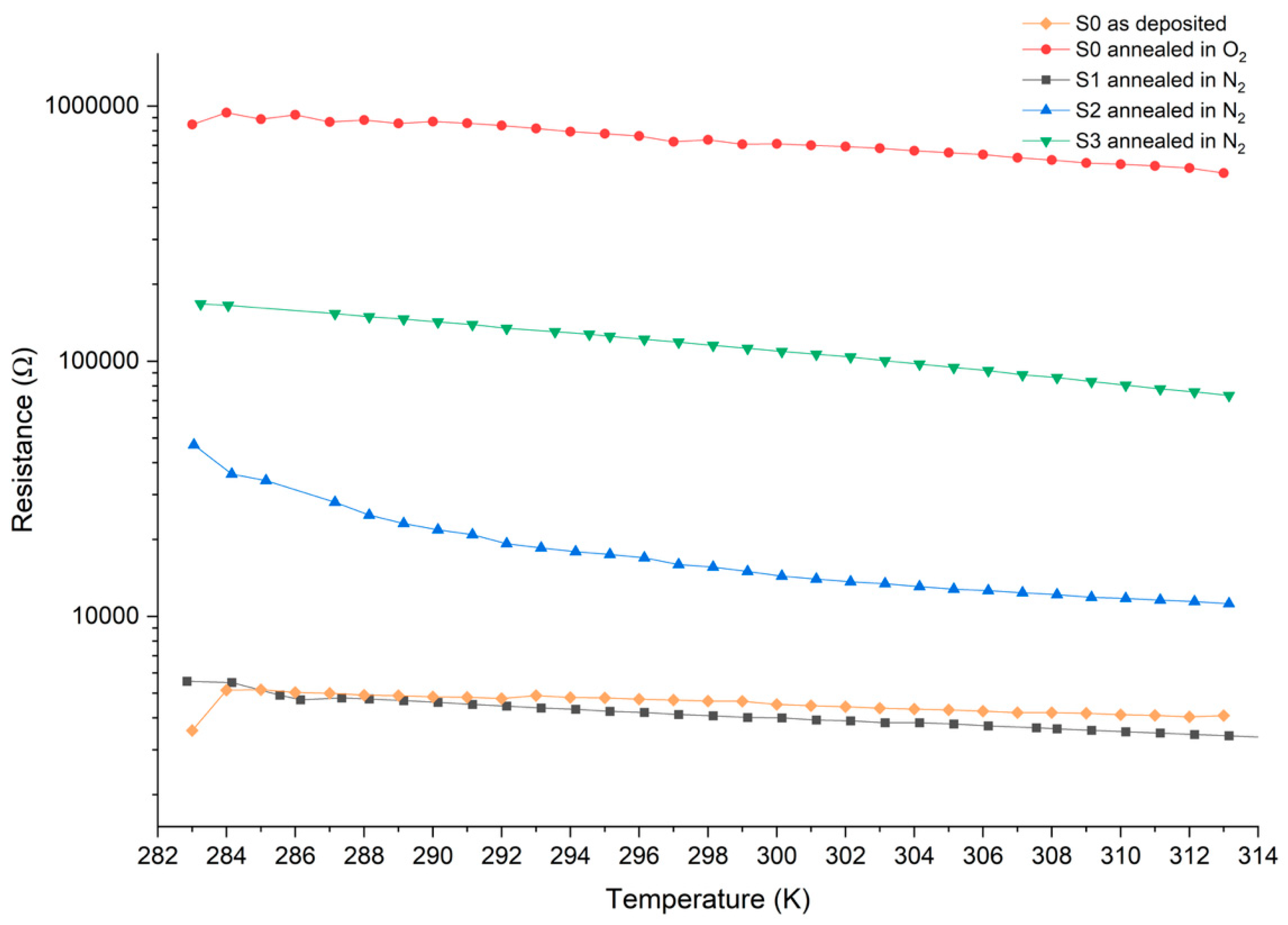
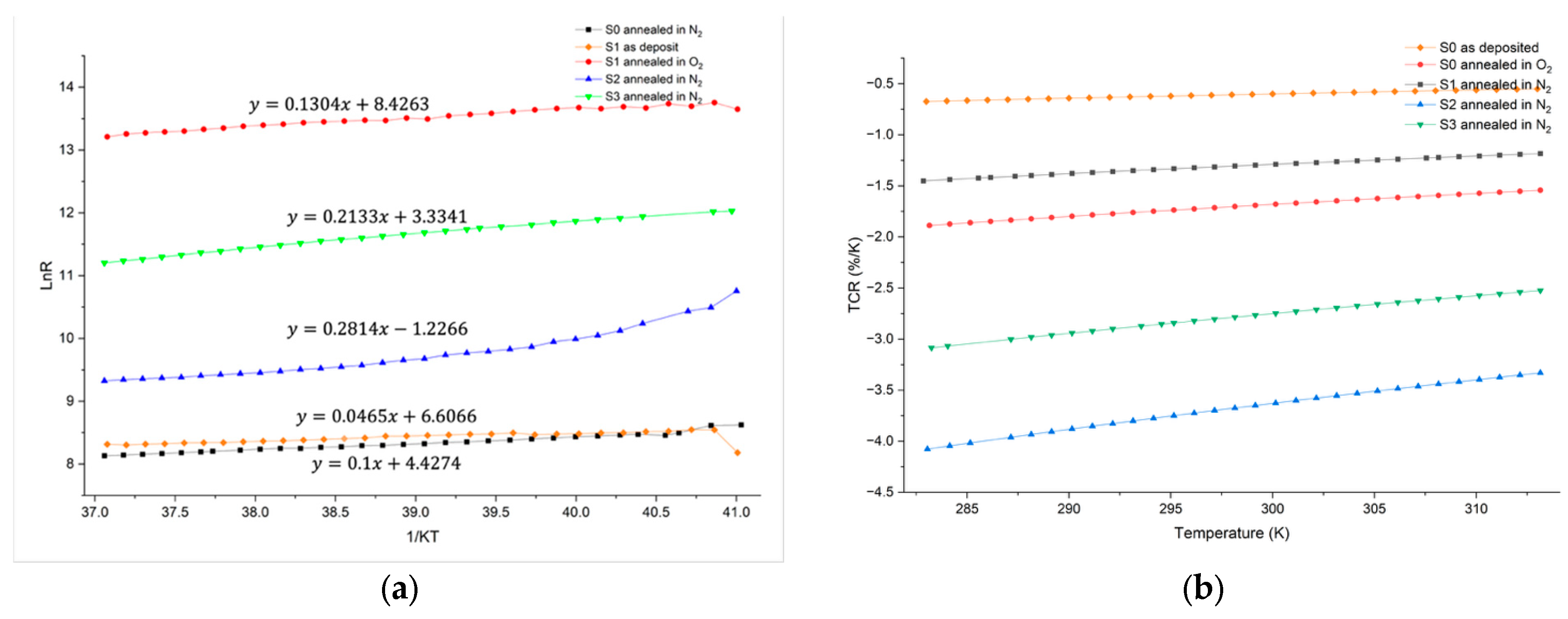
3.5. Resistivity and TCR
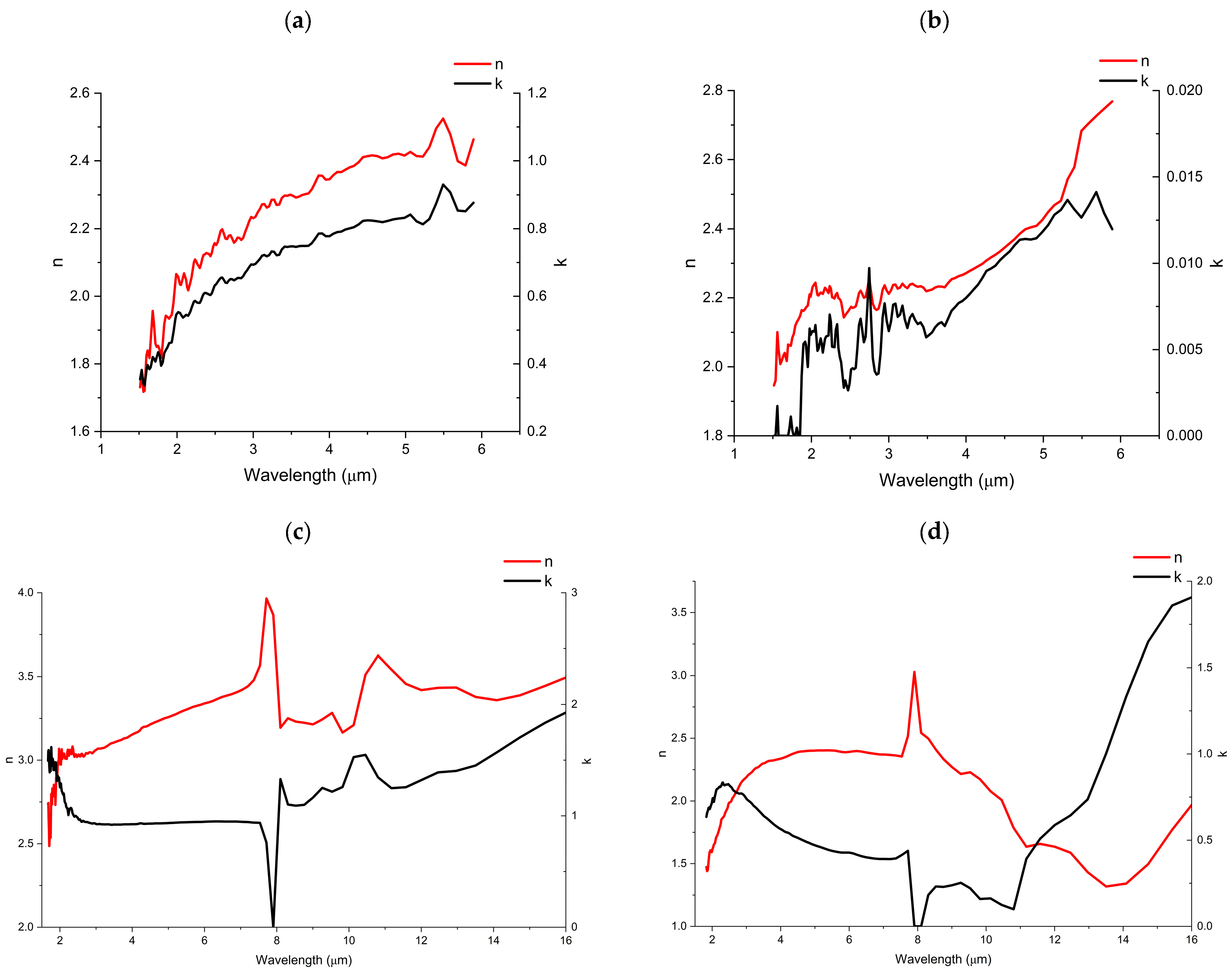
3.6. Optical Constant
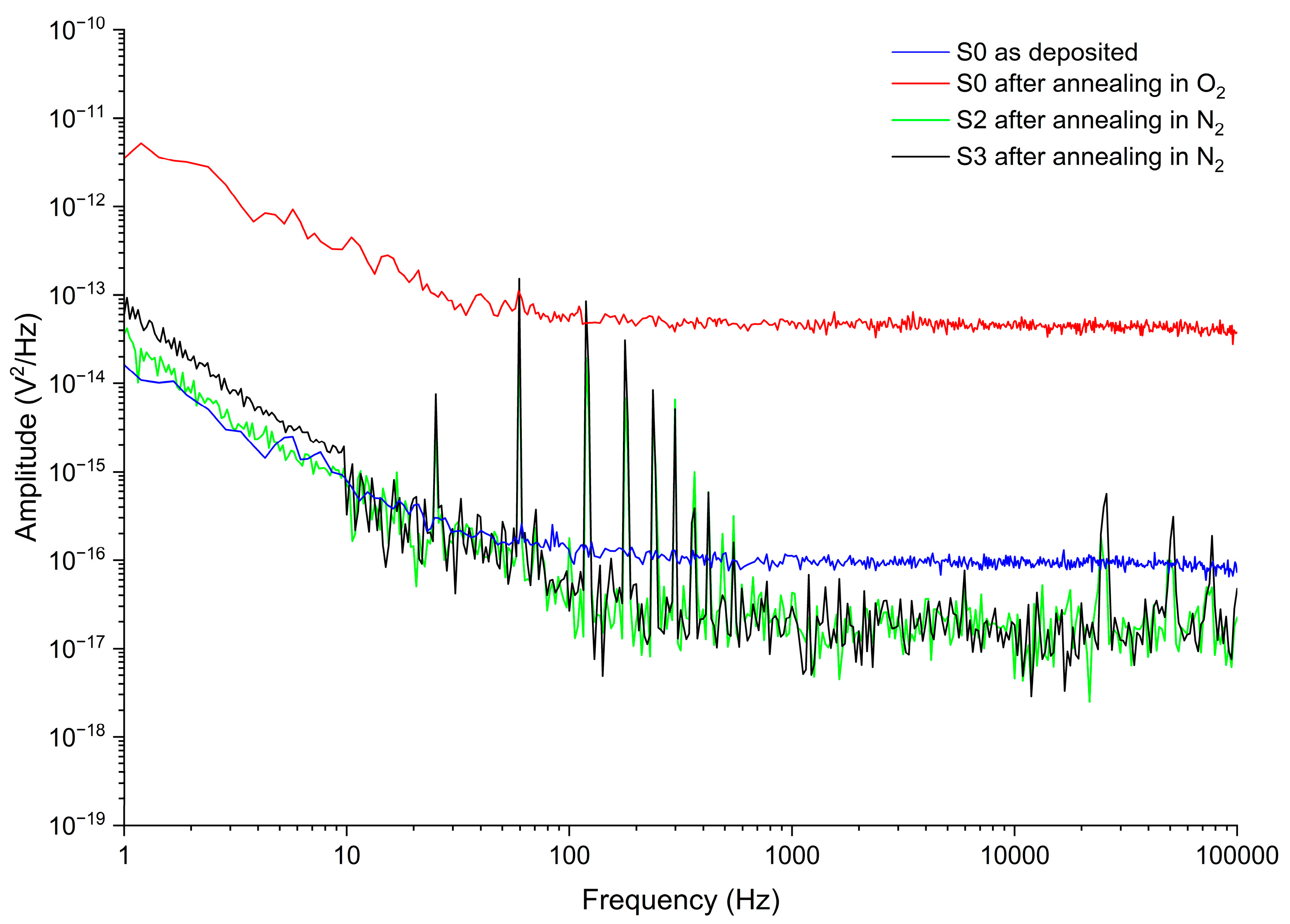
3.7. Noise
4. Conclusions
Author Contributions
Funding
Data Availability Statement
Conflicts of Interest
References
- T., S.P. The Bolometer. Nature 1881, 25, 14–16. [Google Scholar] [CrossRef][Green Version]
- Yadav, P.V.K.; Yadav, I.; Ajitha, B.; Rajasekar, A.; Gupta, S.; Ashok Kumar Reddy, Y. Advancements of uncooled infrared microbolometer materials: A review. Sens. Actuators Phys. 2022, 342, 113611. [Google Scholar] [CrossRef]
- Rogalski, A. History of infrared detectors. Opto-Electron. Rev. 2012, 20, 279–308. [Google Scholar] [CrossRef]
- Rogalski, A. Infrared Detectors, 2nd ed.; Taylor & Francis: Boca Raton, FL, USA, 2010. [Google Scholar] [CrossRef]
- Voshell, A.; Dhar, N.; Rana, M.M. Materials for microbolometers: Vanadium oxide or silicon derivatives. In Image Sensing Technologies: Materials, Devices, Systems, and Applications IV; SPIE: Bellingham, WA, USA, 2017; pp. 92–107. [Google Scholar] [CrossRef]
- Rana, M.M.; Butler, D.P. Radio Frequency sputtered Si1−xGex and Si1−xGexOy thin films for uncooled infrared detectors. Thin Solid Films 2006, 514, 355–360. [Google Scholar] [CrossRef]
- Chen, S.; Lai, J.; Dai, J.; Ma, H.; Wang, H.; Yi, X. Characterization of nanostructured VO2 thin films grown by magnetron controlled sputtering deposition and post annealing method. Opt. Express 2009, 17, 24153–24161. [Google Scholar] [CrossRef]
- Abdel-Rahman, M.; Zia, M.; Alduraibi, M. Temperature-Dependent Resistive Properties of Vanadium Pentoxide/Vanadium Multi-Layer Thin Films for Microbolometer & Antenna-Coupled Microbolometer Applications. Sensors 2019, 19, 1320. [Google Scholar] [CrossRef]
- Kwon, M.-H.; Yang, K.; Park, Y.-S.; Kim, Y.-H.; Chung, H. Investigations of reactively sputtered TiO2-δ films for microbolometer applications. In Electro-Optical and Infrared Systems: Technology and Applications V; SPIE: Bellingham, WA, USA, 2008; pp. 38–47. [Google Scholar] [CrossRef]
- Khan, F.; Julien, C.M.; Islam, S.S. Fabrication of multiwalled carbon nanotubes/MoS2 nanocomposite: Application as temperature sensor. FlatChem 2023, 40, 100521. [Google Scholar] [CrossRef]
- Schneider, K. Optical properties and electronic structure of V2O5, V2O3 and VO2. J. Mater. Sci. Mater. Electron. 2020, 31, 10478–10488. [Google Scholar] [CrossRef]
- Subrahmanyam, A.; Bharat Kumar Reddy, Y.; Nagendra, C.L. Nano-vanadium oxide thin films in mixed phase for microbolometer applications. J. Phys. Appl. Phys. 2008, 41, 195108. [Google Scholar] [CrossRef]
- Vadakepurathu, F.; Rana, M. Electrical, Optical and Thermal Properties of Ge-Si-Sn-O Thin Films. Materials 2024, 17, 3318. [Google Scholar] [CrossRef]
- Rana, M.M.; Butler, D.P. Noise reduction of a-Si1−xGexOy microbolometers by forming gas passivation. Thin Solid Films 2008, 516, 6499–6503. [Google Scholar] [CrossRef]
- Venkatasubramanian, C.; Cabarcos, O.; Allara, D.; Horn, M.; Ashok, S. Correlation of temperature response and structure of annealed VOx thin films for IR detector applications. J. Vac. Sci. Technol. A 2009, 27, 956–961. [Google Scholar] [CrossRef]
- Mellan, T.A.; Grau-Crespo, R. Density functional theory study of rutile VO2 surfaces. J. Chem. Phys. 2012, 137, 154706. [Google Scholar] [CrossRef]
- Petot-Ervas, G.; Farhi, R.; Petot, C. Standard Gibbs free energy of formation of SnO2 from high-temperature e.m.f. measurements. J. Chem. Thermodyn. 1975, 7, 1131–1136. [Google Scholar] [CrossRef]
- Wang, N.; Xue, C.; Wan, F.; Zhao, Y.; Xu, G.; Liu, Z.; Zheng, J.; Zuo, Y.; Cheng, B.; Wang, Q. Spontaneously Conversion from Film to High Crystalline Quality Stripe during Molecular Beam Epitaxy for High Sn Content GeSn. Sci. Rep. 2020, 10, 6161. [Google Scholar] [CrossRef]
- Lin, G.; An, Y.; Ding, H.; Zhao, H.; Wang, J.; Chen, S.; Li, C.; Hickey, R.; Kolodzey, J.; Zeng, Y. Scalable fabrication of self-assembled GeSn vertical nanowires for nanophotonic applications. Nanophotonics 2023, 12, 219–228. [Google Scholar] [CrossRef]
- Kumar, M.; Singh, J.P.; Chae, K.H.; Park, J.; Lee, H.H. Annealing effect on phase transition and thermochromic properties of VO2 thin films. Superlattices Microstruct. 2020, 137, 106335. [Google Scholar] [CrossRef]
- Mazur, M.; Kiełczawa, S.; Domaradzki, J. Effect of Annealing on the Microstructure, Opto-Electronic and Hydrogen Sensing Properties of V2O5 Thin Films Deposited by Magnetron Sputtering. Coatings 2022, 12, 1885. [Google Scholar] [CrossRef]
- Andersson, G.; Paju, J.; Lang, W.; Berndt, W. Studies on Vanadium Oxides. I. Phase Analysis. Acta Chem. Scand. 1953, 8, 1599–1606. [Google Scholar] [CrossRef]
- Pandey, A.; Dalal, S.; Dutta, S.; Dixit, A. Structural characterization of polycrystalline thin films by X-ray diffraction techniques. J. Mater. Sci. Mater. Electron. 2021, 32, 1341–1368. [Google Scholar] [CrossRef]
- Materials Data on SnO2 by Materials Project; LBNL Materials Project; Lawrence Berkeley National Laboratory (LBNL): Berkeley, CA, USA, 2020. [CrossRef]
- Yin, W.; Wolf, S.; Ko, C.; Ramanathan, S.; Reinke, P. Nanoscale probing of electronic band gap and topography of VO2 thin film surfaces by scanning tunneling microscopy. J. Appl. Phys. 2011, 109, 024311. [Google Scholar] [CrossRef]
- Kazmi, J.; Bukhari, S.S.U.H.; Kazmi, J.; Raza, S.R.A.; Shah, J.H.; Jalil, A.; Mohamed, M.A. Thermal annealing and DFT Insights enhance photodetection efficiency in VOx/p-Si heterojunctions. Ceram. Int. 2024, 50, 46042–46050. [Google Scholar] [CrossRef]
- Markvart, T.; Castaner, L. Semiconductor Materials and Modelling. In Practical Handbook of Photovoltaics; Academic Press: Cambridge, MA, USA, 2012; pp. 33–62. [Google Scholar] [CrossRef]
- Pajot, B. Optical Absorption of Impurities and Defects in Semiconducting Crystals: Hydrogen-Like Centres; Springer Series in Solid-State Sciences; Springer: Berlin/Heidelberg, Germany, 2010. [Google Scholar]
- Luo, Z.; Wu, Z.; Xu, X.; Wang, T.; Jiang, Y. Electrical and optical properties of nanostructured VOX thin films prepared by direct current magnetron reactive sputtering and post-annealing in oxygen. Thin Solid Films 2011, 519, 6203–6207. [Google Scholar] [CrossRef]
- Zhang, Z.; Zuo, F.; Wan, C.; Dutta, A.; Kim, J.; Rensberg, J.; Nawrodt, R.; Park, H.H.; Larrabee, T.J.; Guan, X.; et al. Evolution of Metallicity in Vanadium Dioxide by Creation of Oxygen Vacancies. Phys. Rev. Appl. 2017, 7, 034008. [Google Scholar] [CrossRef]
- Karmaoui, M.; Jorge, A.B.; McMillan, P.F.; Aliev, A.E.; Pullar, R.C.; Labrincha, J.A.; Tobaldi, D.M. One-Step Synthesis, Structure, and Band Gap Properties of SnO2 Nanoparticles Made by a Low Temperature Nonaqueous Sol–Gel Technique. ACS Omega 2018, 3, 13227–13238. [Google Scholar] [CrossRef]
- Rajendra Kumar, R.T.; Karunagaran, B.; Mangalaraj, D.; Narayandass, S.K.; Manoravi, P.; Joseph, M.; Gopal, V. Pulsed laser deposited vanadium oxide thin films for uncooled infrared detectors. Sens. Actuators Phys. 2003, 107, 62–67. [Google Scholar] [CrossRef]
- Su, Y.-Y.; Cheng, X.-W.; Li, J.-B.; Dou, Y.-K.; Rehman, F.; Su, D.-Z.; Jin, H.-B. Evolution of microstructure in vanadium oxide bolometer film during annealing process. Appl. Surf. Sci. 2015, 357, 887–891. [Google Scholar] [CrossRef]
- Gauntt, B.D.; Li, J.; Cabarcos, O.M.; Basantani, H.A.; Venkatasubramanian, C.; Bharadwaja, S.S.N.; Podraza, N.J.; Jackson, T.N.; Allara, D.L.; Antrazi, S.; et al. Microstructure of vanadium oxide used in microbolometers. In Infrared Technology and Applications XXXVII; SPIE: Bellingham, WA, USA, 2011; pp. 1218–1224. [Google Scholar] [CrossRef]
- Tien, C.-L.; Chiang, C.-Y.; Wang, C.-C.; Lin, S.-C. Optical, Electrical, Structural, and Thermo-Mechanical Properties of Undoped and Tungsten-Doped Vanadium Dioxide Thin Films. Materials 2024, 17, 2382. [Google Scholar] [CrossRef]
- Ozcelik, A.; Cabarcos, O.; Allara, D.L.; Horn, M.W. Vanadium Oxide Thin Films Alloyed with Ti, Zr, Nb, and Mo for Uncooled Infrared Imaging Applications. J. Electron. Mater. 2013, 42, 901–905. [Google Scholar] [CrossRef]
- Liu, K.; Lee, S.; Yang, S.; Delaire, O.; Wu, J. Recent progresses on physics and applications of vanadium dioxide. Mater. Today 2018, 21, 875–896. [Google Scholar] [CrossRef]
- Uberuaga, B.P.; Vernon, L.J.; Martinez, E.; Voter, A.F. The relationship between grain boundary structure, defect mobility and grain boundary sink efficiency. Sci. Rep. 2015, 5, 9095. [Google Scholar] [CrossRef]
- Weisberg, L.R. Anomalous Mobility Effects in Some Semiconductors and Insulators. J. Appl. Phys. 1962, 33, 1817–1821. [Google Scholar] [CrossRef]
- McWhan, D.B.; Marezio, M.; Remeika, J.P.; Dernier, P.D. X-ray diffraction study of metallic VO2. Phys. Rev. B 1974, 10, 490–495. [Google Scholar] [CrossRef]
- Brückner, W.; Moldenhauer, W.; Wich, H.; Wolf, E.; Oppermann, H.; Gerlach, U.; Reichelt, W. The range of homogeneity of VO2 and the influence of the composition on the physical properties. II. The change of the physical properties in the range of homogeneity. Phys. Status Solidi A 1975, 29, 63–70. [Google Scholar] [CrossRef]
- Scott, E.A.; Singh, M.K.; Barber, J.P.; Rost, C.M.; Ivanov, S.; Watt, J.; Pete, D.; Sharma, P.; Lu, T.-M.; Harris, C.T. Sensing performance of sub-100-nm vanadium oxide films for room temperature thermal detection applications. Appl. Phys. Lett. 2022, 121, 203505. [Google Scholar] [CrossRef]
- Wan, C.; Zhang, Z.; Woolf, D.; Hessel, C.M.; Rensberg, J.; Hensley, J.M.; Xiao, Y.; Shahsafi, A.; Salman, J.; Richter, S.; et al. Optical properties of thin-film vanadium dioxide from the visible to the far infrared. Ann. Phys. 2019, 531, 1900188. [Google Scholar] [CrossRef]
- Lamsal, C.; Ravindra, N.M. Vanadium Oxides: Synthesis, Properties, and Applications. In Semiconductors: Synthesis, Properties and Applications; Pech-Canul, M.I., Ravindra, N.M., Eds.; Springer International Publishing: Cham, Switzerland, 2019; pp. 127–218. [Google Scholar] [CrossRef]
- Atuchin, V.V.; Ayupov, B.M.; Kochubey, V.A.; Pokrovsky, L.D.; Ramana, C.V.; Rumiantsev, Y.M. Optical properties of textured V2O5/Si thin films deposited by reactive magnetron sputtering. Opt. Mater. 2008, 30, 1145–1148. [Google Scholar] [CrossRef]
- Esther, A.C.M.; Porwal, D.; Pradeepkumar, M.S.; Rangappa, D.; Sharma, A.K.; Dey, A. Optical constants of pulsed RF magnetron sputtered nanocolumner V2O5 coating. Phys. B Condens. Matter 2015, 478, 161–166. [Google Scholar] [CrossRef]
- Hooge, F.N. 1/f noise sources. IEEE Trans. Electron Devices 1994, 41, 1926–1935. [Google Scholar] [CrossRef]
- Abdel-Rahman, M.; Al-Khalli, N.; Zia, M.F.; Alduraibi, M.; Ilahi, B.; Awad, E.; Debbar, N. Fabrication and design of vanadium oxide microbolometer. AIP Conf. Proc. 2017, 1809, 020001. [Google Scholar] [CrossRef]
- Kumar, R.T.R.; Karunagaran, B.; Mangalaraj, D.; Narayandass, S.K.; Manoravi, P.; Joseph, M.; Gopal, V.; Madaria, R.K.; Singh, J.P. Room temperature deposited vanadium oxide thin films for uncooled infrared detectors. Mater. Res. Bull. 2003, 38, 1235–1240. [Google Scholar] [CrossRef]



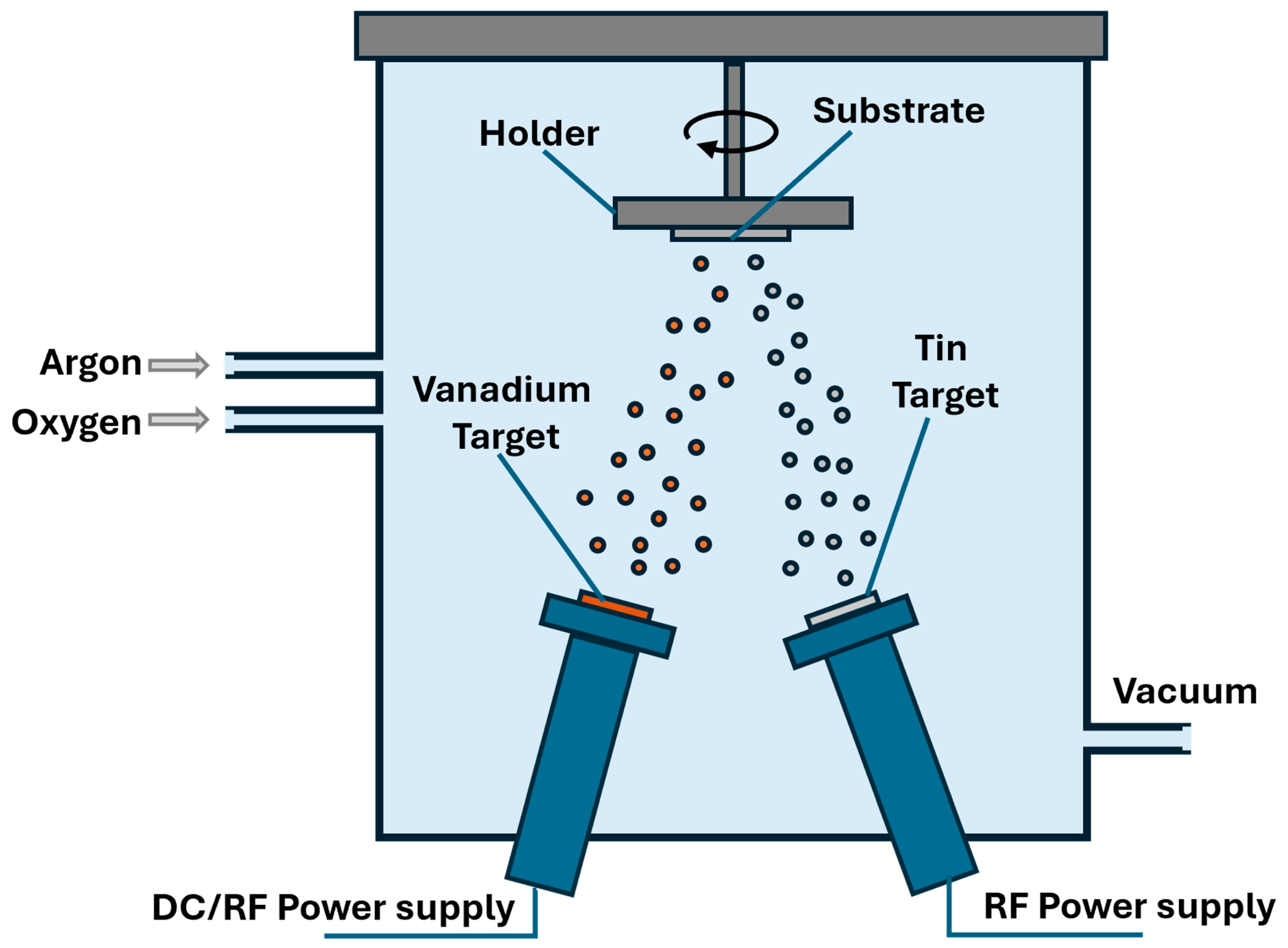
| Sample ID | V Target Power (W) | Sn Target Power (W) | O2 Partial Pressure | Deposition Temperature (°C) | Post-Annealing Environment | Atomic Compositions |
|---|---|---|---|---|---|---|
| S0 (Torr) | 50 (RF) | 6 | 3% | Room Temperature | O2 | V0.40Sn0.1O0.5 |
| S1 (AJA International) | 200 (DC) | 0 | 5% | 450 | N2 | V0.53O0.47 |
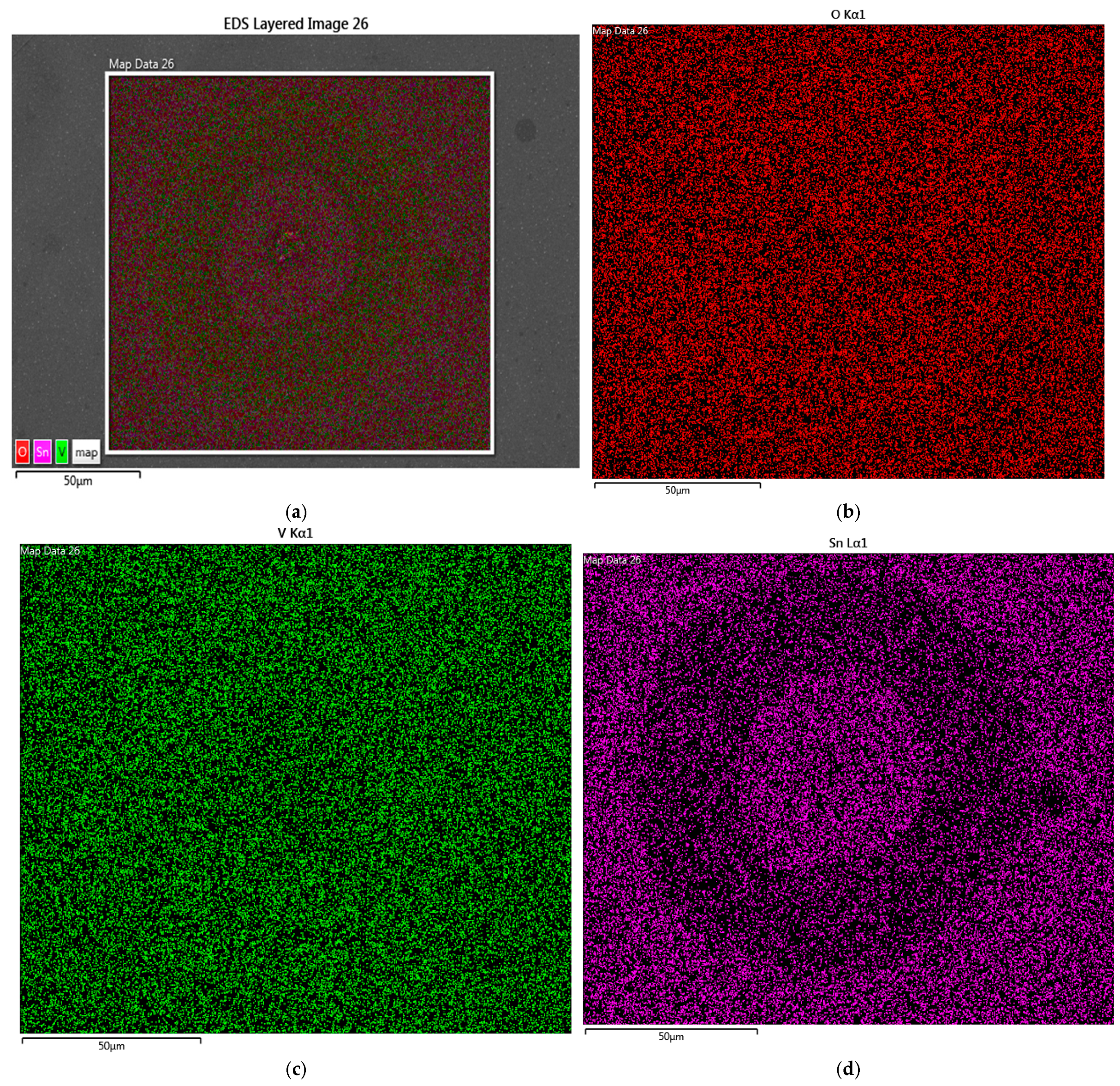
| S2 (AJA International) | 200 (DC) | 10 | 5% | 450 | N2 | V0.46Sn0.03O0.51 |
| S3 (AJA International) | 200 (DC) | 30 | 5% | 450 | N2 | V0.37Sn0.13O0.5 |
| Sample ID | Annealing Environment | Thickness (nm) | Ra (nm) | RS (nm) |
|---|---|---|---|---|
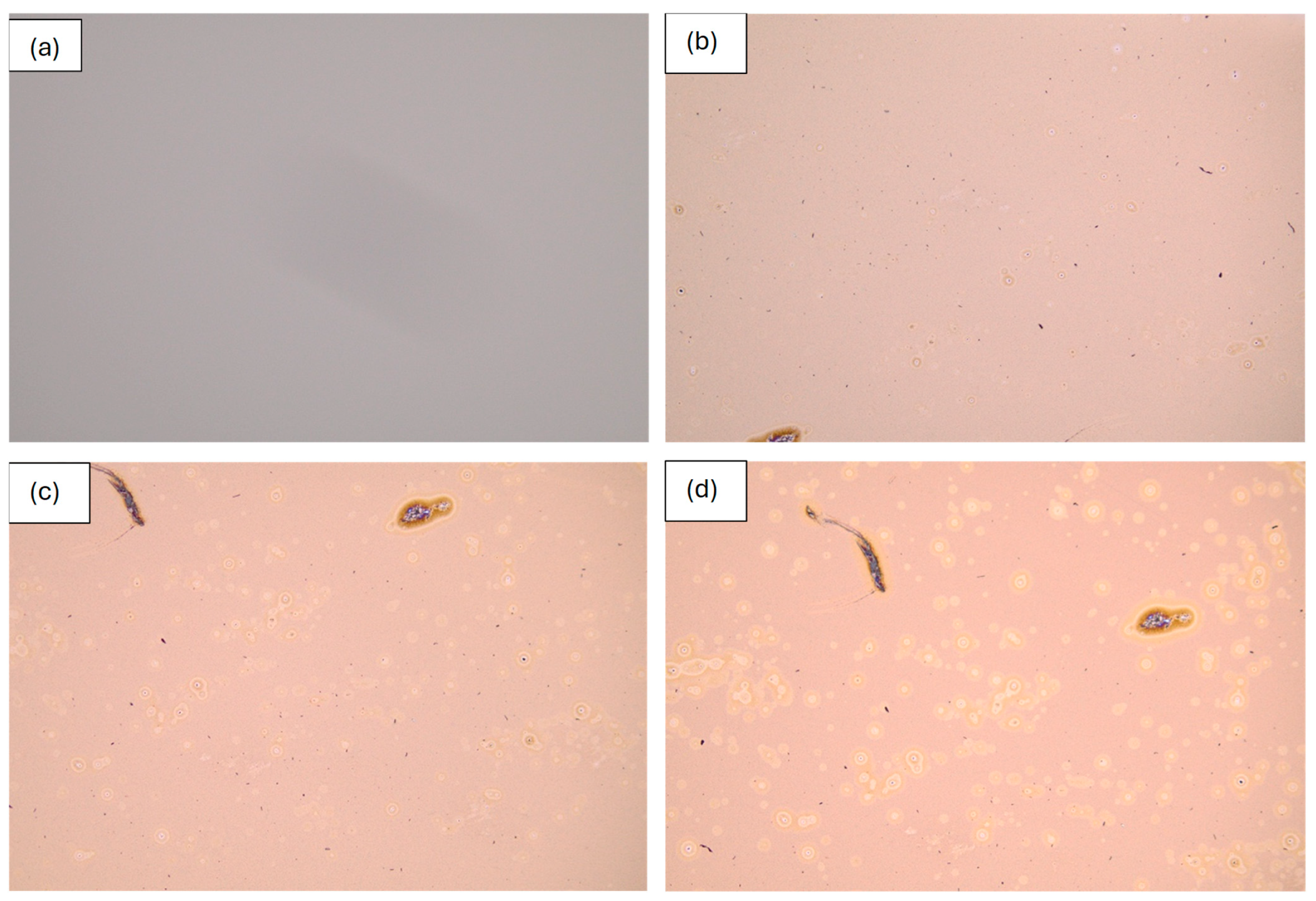
| S0 as deposited | None | 151.2 | 2.63 | 3.5 |
| S0 after annealing | O2 | 645 | 139 | 180 |
| S2 as deposited | None | 120 | 6.9 | 8.4 |
| S2 after annealing | N2 | 135 | 7.07 | 17.3 |
| Sample ID | Sn% | Phase | Annealing Environment | Resistivity (Ω⋅cm) |
|---|---|---|---|---|
| S1 | 0 | VO2 | N2 | 6.19 × 10⁻² |
| S2 | 3% | VO2 | N2 | 7.3 × 10⁻² |
| S3 | 13% | VO2 and SnO2 | N2 | 2.47 × 10⁻¹ |
| S0 | 10% | V2O5 and SnO2 | O2 | 5.24 |
| Materials | Bandgap (eV) | Resistivity (Ω⋅cm) | TCR (%/K) | Noise Voltage PSD | Reference |
|---|---|---|---|---|---|
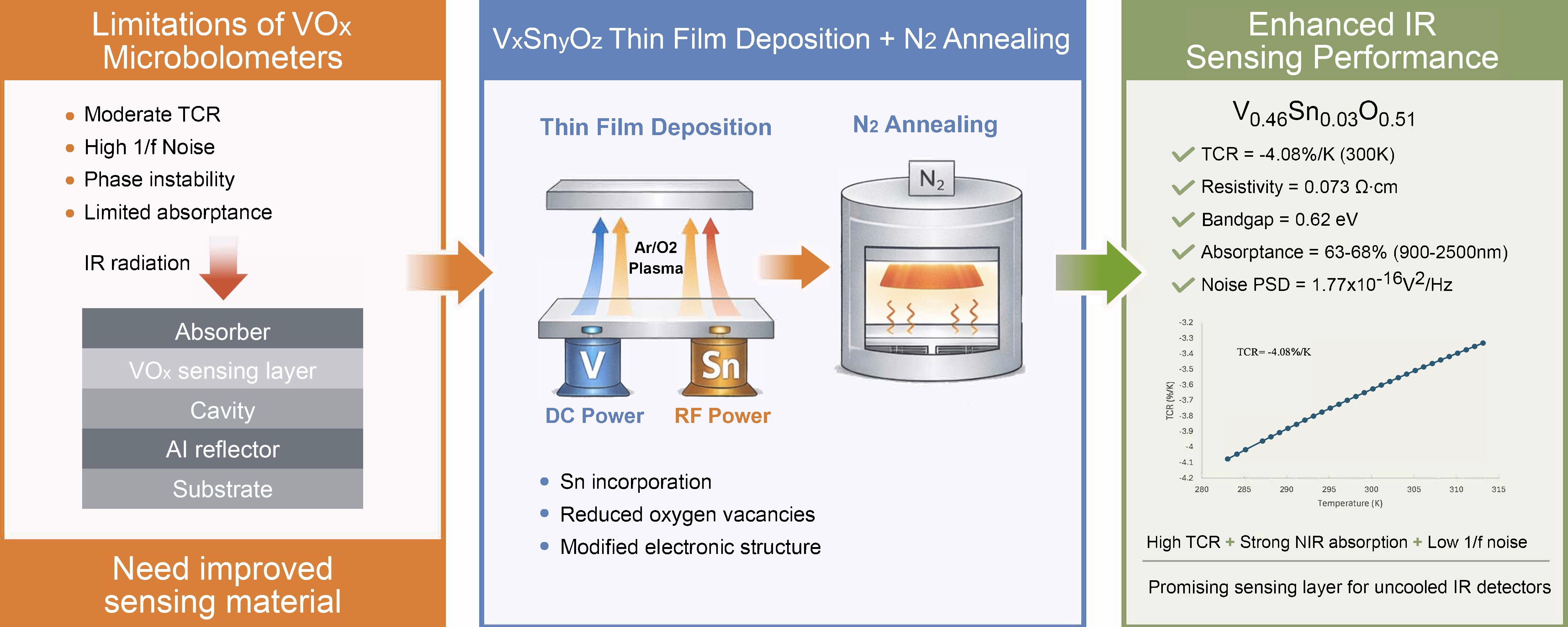
| V0.46Sn0.03O0.51 | 0.62 | 0.073 | −4.08 | 3.66 × 10⁻¹⁴ V2/Hz at 1 Hz to 1.77 × 10⁻¹⁶ V2/Hz at 100 Hz | Current work |
| V2O5/V | N/A | 0.047 | −3.18 | 1.32 × 10⁻⁹ V2/Hz at 12 Hz | Abdel-Rahman et al. [8,46] |
| VOx | N/A | 10−3 to 6.8 × 10⁴ | 0 to −4 | N/A | Gauntt et al. [34] |
| VOx | N/A | 10−2 | −2.54 | N/A | Scott et al. [42] |
| VxMoyOz | ~1 Ω·cm | −1.7 to −2.2 | Ozcelik et al. [36] | ||
| VxTiyOz | ~1 Ω·cm | −1.6 | |||
| VxZryOz | ~1 Ω·cm | −1.9 to −2.7 | |||
| a-Si | N/A | 5000 | −3.7 | N/A | Voshell et al. [5] |
| SiGeO | 0.75 to 0.89 | N/A | −3.5 to −8.7 | N/A | Rana et al. [6] |
| GeSiSnO | 1.03 | 1.464 × 10⁻³ | −3.26 | 1.76 × 10⁻¹¹ V2/Hz at 2 Hz to 2.28 × 10⁻¹² V2/Hz at 10 Hz | Vadakepurathu et al. [13] |
| TiO2 | N/A | 0.01 to 10 | −2.8 | N/A | Kwon et al. [9] |
Disclaimer/Publisher’s Note: The statements, opinions and data contained in all publications are solely those of the individual author(s) and contributor(s) and not of MDPI and/or the editor(s). MDPI and/or the editor(s) disclaim responsibility for any injury to people or property resulting from any ideas, methods, instructions or products referred to in the content. |
© 2026 by the authors. Licensee MDPI, Basel, Switzerland. This article is an open access article distributed under the terms and conditions of the Creative Commons Attribution (CC BY) license.
Share and Cite
Cong, L.; Rana, M. Effect of Annealing on Electrical and Optical Properties of Tin-Doped Vanadium Oxide Films for Microbolometer Applications. Nanomaterials 2026, 16, 504. https://doi.org/10.3390/nano16090504
Cong L, Rana M. Effect of Annealing on Electrical and Optical Properties of Tin-Doped Vanadium Oxide Films for Microbolometer Applications. Nanomaterials. 2026; 16(9):504. https://doi.org/10.3390/nano16090504
Chicago/Turabian StyleCong, Lin, and Mukti Rana. 2026. "Effect of Annealing on Electrical and Optical Properties of Tin-Doped Vanadium Oxide Films for Microbolometer Applications" Nanomaterials 16, no. 9: 504. https://doi.org/10.3390/nano16090504
APA StyleCong, L., & Rana, M. (2026). Effect of Annealing on Electrical and Optical Properties of Tin-Doped Vanadium Oxide Films for Microbolometer Applications. Nanomaterials, 16(9), 504. https://doi.org/10.3390/nano16090504