Recent Advances in Diamond-Capped GaN HEMTs for RF Application

 , , ,
, , ,  , ,
, ,
Abstract
1. Introduction
2. Diamond Film Growth and Interface Optimization
2.1. Optimization of Diamond Film Growth
2.1.1. Nucleation Technology
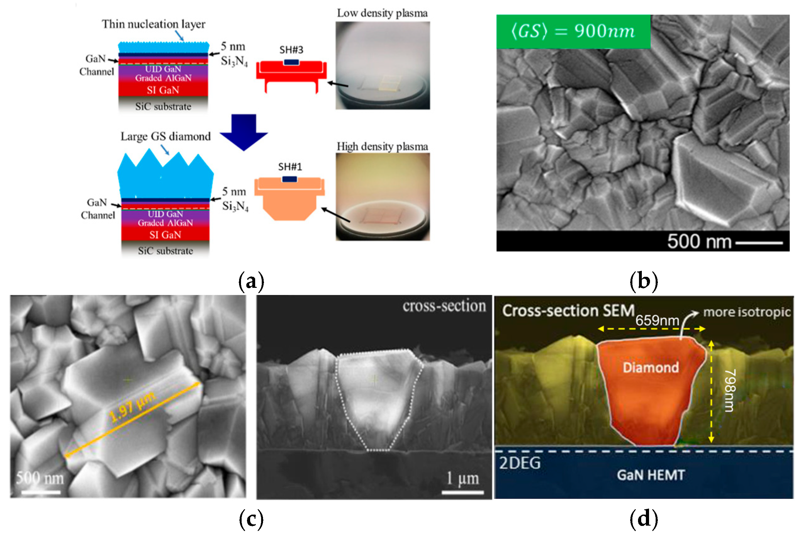
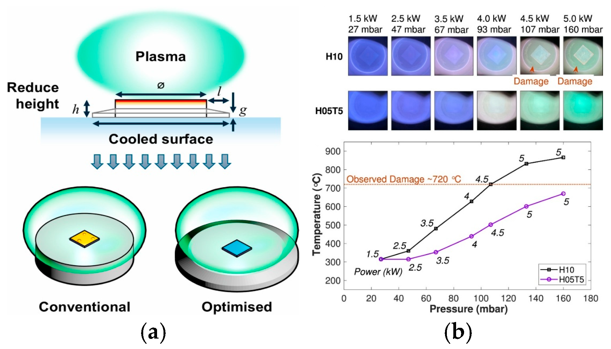
2.1.2. Growth Stage Optimization
2.2. Optimization of TBR at the Diamond/GaN Interface
2.2.1. Interlayer Optimization
2.2.2. Interface Structure Optimization
3. Simulation of Diamond-Capped GaN HEMTs
4. Key Fabrication Processes
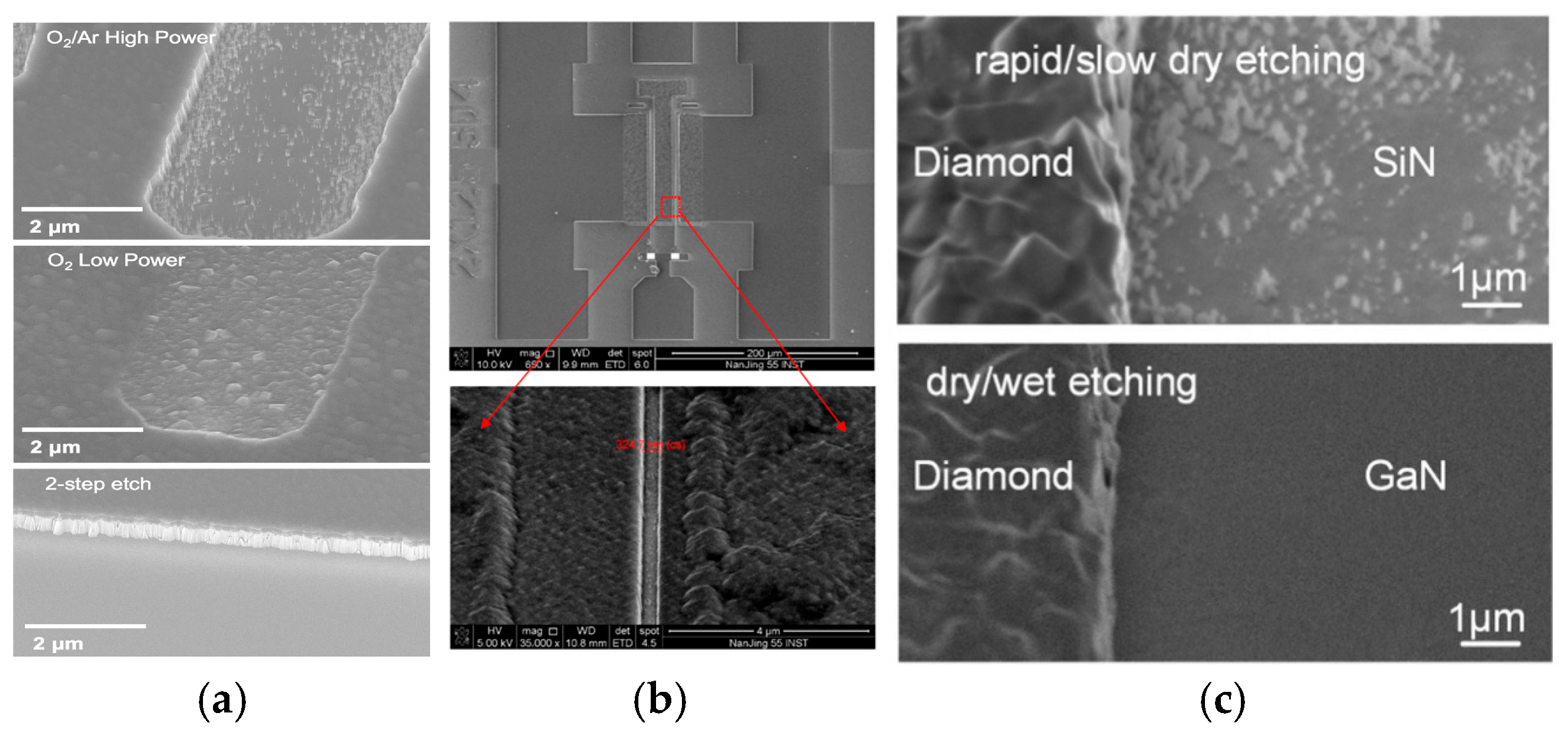
4.1. Diamond Etching
4.2. Process Integration Routes of Diamond-Capped GaN HEMTs
5. Future Perspectives
6. Conclusions
Author Contributions
Funding
Data Availability Statement
Conflicts of Interest
References
- Asif Khan, M.; Bhattarai, A.; Kuznia, J.N.; Olson, D.T. High electron mobility transistor based on a GaN-AlxGa1−xN heterojunction. Appl. Phys. Lett. 1993, 63, 1214–1215. [Google Scholar] [CrossRef]
- Vurgaftman, I.; Meyer, J.R.; Ram-Mohan, L.R. Band parameters for III–V compound semiconductors and their alloys. J. Appl. Phys. 2001, 89, 5815–5875. [Google Scholar] [CrossRef]
- Millán, J.; Godignon, P.; Perpiñà, X.; Pérez-Tomás, A.; Rebollo, J. A Survey of Wide Bandgap Power Semiconductor Devices. IEEE Trans. Power Electron. 2014, 29, 2155–2163. [Google Scholar] [CrossRef]
- Roccaforte, F.; Fiorenza, P.; Greco, G.; Lo Nigro, R.; Giannazzo, F.; Iucolano, F.; Saggio, M. Emerging trends in wide band gap semiconductors (SiC and GaN) technology for power devices. Microelectron. Eng. 2018, 187–188, 66–77. [Google Scholar] [CrossRef]
- Nakajima, S. GaN HEMTs for 5G Base Station Applications. In Proceedings of the 2018 IEEE International Electron Devices Meeting (IEDM), San Francisco, CA, USA, 1–5 December 2018; pp. 14.12.11–14.12.14. [Google Scholar]
- Mao, M.; Tang, S.; Wang, Z.; Deng, R.; Deng, C.; Chen, S.; Ren, Y. Effect of Temperature Cycling, High Temperature Storage and Steady-State Operation Life Test on Reliability of GaN HEMTs. In Proceedings of the 2021 22nd International Conference on Electronic Packaging Technology (ICEPT), Xiamen, China, 14–17 September 2021; pp. 1–4. [Google Scholar]
- Zhu, S.; Liu, Y.; Xiao, Z.; Huang, L.; Wu, Q.; Mao, S.; Wang, H.; Xu, Y. A Ku-Band 40W GaN Power Amplifier MMIC for Satellite Communication. In Proceedings of the 2022 IEEE MTT-S International Microwave Workshop Series on Advanced Materials and Processes for RF and THz Applications (IMWS-AMP), Guangzhou, China, 27–29 November 2022; pp. 1–3. [Google Scholar]
- Asif Khan, M.; Kuznia, J.N.; Olson, D.T.; Schaff, W.J.; Burm, J.W.; Shur, M.S. Microwave performance of a 0.25 μm gate AlGaN/GaN heterostructure field effect transistor. Appl. Phys. Lett. 1994, 65, 1121–1123. [Google Scholar] [CrossRef]
- Wu, Y.F.; Saxler, A.; Moore, M.; Smith, R.P.; Sheppard, S.; Chavarkar, P.M.; Wisleder, T.; Mishra, U.K.; Parikh, P. 30-W/mm GaN HEMTs by field plate optimization. IEEE Electron Device Lett. 2004, 25, 117–119. [Google Scholar] [CrossRef]
- Tadjer, M.J.; Anderson, T.J.; Ancona, M.G.; Raad, P.E.; Komarov, P.; Bai, T.; Gallagher, J.C.; Koehler, A.D.; Goorsky, M.S.; Francis, D.A.; et al. GaN-On-Diamond HEMT Technology With TAVG = 176 °C at PDC, max = 56 W/mm Measured by Transient Thermoreflectance Imaging. IEEE Electron Device Lett. 2019, 40, 881–884. [Google Scholar] [CrossRef]
- Zhou, H.; Zhang, C.; Zhang, K.; Huang, Z.; Liu, F.; Zhou, M.; Gong, H.; Tang, S.; Liu, W.; Wang, B.; et al. High power density gallium nitride radio frequency transistors via enhanced nucleation in heteroepitaxy. Nat. Commun. 2025, 17, 556. [Google Scholar] [CrossRef]
- Zhang, Y.; Feng, S.; Zhu, H.; Zhang, J.; Deng, B. Two-dimensional transient simulations of the self-heating effects in GaN-based HEMTs. Microelectron. Reliab. 2013, 53, 694–700. [Google Scholar] [CrossRef]
- Kebir, M.E.; Bri, S. Self-Heating in the HEMT AlGaN/GaN transistor. In Proceedings of the 2020 IEEE 2nd International Conference on Electronics, Control, Optimization and Computer Science (ICECOCS), Kenitra, Morocco, 2–3 December 2020; pp. 1–6. [Google Scholar]
- Aminbeidokhti, A.; Dimitrijev, S.; Hanumanthappa, A.K.; Moghadam, H.A.; Haasmann, D.; Han, J.; Shen, Y.; Xu, X. Gate-Voltage Independence of Electron Mobility in Power AlGaN/GaN HEMTs. IEEE Trans. Electron Devices 2016, 63, 1013–1019. [Google Scholar] [CrossRef]
- Chae, M.; Cha, H.Y.; Kim, H. Abnormal Temperature and Bias Dependence of Threshold Voltage Instability in p-GaN/AlGaN/GaN HEMTs. IEEE J. Electron Devices Soc. 2024, 12, 581–586. [Google Scholar] [CrossRef]
- Zeng, C.; Wang, Y.S.; Liao, X.Y.; Li, R.G.; Chen, Y.Q.; Lai, P.; Huang, Y.; En, Y.F. Reliability Investigations of AlGaN/GaN HEMTs Based on On-State Electroluminescence Characterization. IEEE Trans. Device Mater. Reliab. 2015, 15, 69–74. [Google Scholar] [CrossRef]
- Graebner, J.E.; Reiss, M.E.; Seibles, L.; Hartnett, T.M.; Miller, R.P.; Robinson, C.J. Phonon scattering in chemical-vapor-deposited diamond. Phys. Rev. B 1994, 50, 3702–3713. [Google Scholar] [CrossRef] [PubMed]
- May, P.W. Diamond thin films: A 21st-century material. Philos. Trans. R. Soc. A Math. Phys. Eng. Sci. 2000, 358, 473–495. [Google Scholar] [CrossRef]
- Fan, K.; Guo, J.; Huang, Z.; Xu, Y.; Huang, Z.; Xu, W.; Wang, Q.; Lin, Q.; Li, X.; Liu, H.; et al. GaN-on-diamond technology for next-generation power devices. Moore More 2025, 1, 370–394. [Google Scholar] [CrossRef]
- Zheng, X.-F.; Wang, A.-C.; Hou, X.-H.; Wang, Y.-Z.; Wen, H.-Y.; Wang, C.; Lu, Y.; Mao, W.; Ma, X.-H.; Hao, Y. Influence of the Diamond Layer on the Electrical Characteristics of AlGaN/GaN High-Electron-Mobility Transistors. Chin. Phys. Lett. 2017, 34, 027301. [Google Scholar] [CrossRef]
- Lu, M.C. Development of Diamond Device-Level Heat Spreader for the Advancement of GaN HEMT Power and RF Electronics. IEEE Trans. Device Mater. Reliab. 2023, 23, 468–485. [Google Scholar] [CrossRef]
- Seelmann-Eggebert, M.; Meisen, P.; Schaudel, F.; Koidl, P.; Vescan, A.; Leier, H. Heat-spreading diamond films for GaN-based high-power transistor devices. Diam. Relat. Mater. 2001, 10, 744–749. [Google Scholar] [CrossRef]
- Alomari, M.; Dipalo, M.; Rossi, S.; Diforte-Poisson, M.A.; Delage, S.; Carlin, J.F.; Grandjean, N.; Gaquiere, C.; Toth, L.; Pecz, B.; et al. Diamond overgrown InAlN/GaN HEMT. Diam. Relat. Mater. 2011, 20, 604–608. [Google Scholar] [CrossRef]
- Mu, F.; He, R.; Suga, T. Room temperature GaN-diamond bonding for high-power GaN-on-diamond devices. Scr. Mater. 2018, 150, 148–151. [Google Scholar] [CrossRef]
- Liang, J.; Kobayashi, A.; Shimizu, Y.; Ohno, Y.; Kim, S.W.; Koyama, K.; Kasu, M.; Nagai, Y.; Shigekawa, N. Fabrication of GaN/Diamond Heterointerface and Interfacial Chemical Bonding State for Highly Efficient Device Design. Adv. Mater. 2021, 33, e2104564. [Google Scholar] [CrossRef]
- Zhou, Y.; Ramaneti, R.; Anaya, J.; Korneychuk, S.; Derluyn, J.; Sun, H.; Pomeroy, J.; Verbeeck, J.; Haenen, K.; Kuball, M. Thermal characterization of polycrystalline diamond thin film heat spreaders grown on GaN HEMTs. Appl. Phys. Lett. 2017, 111, 041901. [Google Scholar] [CrossRef]
- Jia, X.; Wei, J.-J.; Kong, Y.; Li, C.-M.; Liu, J.; Chen, L.; Sun, F.; Wang, X. The influence of dielectric layer on the thermal boundary resistance of GaN-on-diamond substrate. Surf. Interface Anal. 2019, 51, 783–790. [Google Scholar] [CrossRef]
- Middleton, C.; Chandrasekar, H.; Singh, M.; Pomeroy, J.W.; Uren, M.J.; Francis, D.; Kuball, M. Impact of thinning the GaN buffer and interface layer on thermal and electrical performance in GaN-on-diamond electronic devices. Appl. Phys. Express 2019, 12, 024003. [Google Scholar] [CrossRef]
- Angadi, M.A.; Watanabe, T.; Bodapati, A.; Xiao, X.; Auciello, O.; Carlisle, J.A.; Eastman, J.A.; Keblinski, P.; Schelling, P.K.; Phillpot, S.R. Thermal transport and grain boundary conductance in ultrananocrystalline diamond thin films. J. Appl. Phys. 2006, 99, 114301. [Google Scholar] [CrossRef]
- Anaya, J.; Rossi, S.; Alomari, M.; Kohn, E.; Tóth, L.; Pécz, B.; Kuball, M. Thermal conductivity of ultrathin nano-crystalline diamond films determined by Raman thermography assisted by silicon nanowires. Appl. Phys. Lett. 2015, 106, 223101. [Google Scholar] [CrossRef]
- Anaya, J.; Rossi, S.; Alomari, M.; Kohn, E.; Tóth, L.; Pécz, B.; Hobart, K.D.; Anderson, T.J.; Feygelson, T.I.; Pate, B.B.; et al. Control of the in-plane thermal conductivity of ultra-thin nanocrystalline diamond films through the grain and grain boundary properties. Acta Mater. 2016, 103, 141–152. [Google Scholar] [CrossRef]
- Malakoutian, M.; Ren, C.; Woo, K.; Li, H.; Chowdhury, S. Development of Polycrystalline Diamond Compatible with the Latest N-Polar GaN mm-Wave Technology. Cryst. Growth Des. 2021, 21, 2624–2632. [Google Scholar] [CrossRef]
- Meyer, D.J.; Feygelson, T.I.; Anderson, T.J.; Roussos, J.A.; Tadjer, M.J.; Downey, B.P.; Katzer, D.S.; Pate, B.B.; Ancona, M.G.; Koehler, A.D.; et al. Large-Signal RF Performance of Nanocrystalline Diamond Coated AlGaN/GaN High Electron Mobility Transistors. IEEE Electron Device Lett. 2014, 35, 1013–1015. [Google Scholar] [CrossRef]
- Ahmed, R.; Siddique, A.; Anderson, J.; Engdahl, C.; Holtz, M.; Piner, E. Selective Area Deposition of Hot Filament CVD Diamond on 100 mm MOCVD Grown AlGaN/GaN Wafers. Cryst. Growth Des. 2019, 19, 672–677. [Google Scholar] [CrossRef]
- Malakoutian, M.; Zheng, X.; Woo, K.; Soman, R.; Kasperovich, A.; Pomeroy, J.; Kuball, M.; Chowdhury, S. Low Thermal Budget Growth of Near-Isotropic Diamond Grains for Heat Spreading in Semiconductor Devices. Adv. Funct. Mater. 2022, 32, 2208997. [Google Scholar] [CrossRef]
- Sun, H.; Pomeroy, J.W.; Simon, R.B.; Francis, D.; Faili, F.; Twitchen, D.J.; Kuball, M. Temperature-Dependent Thermal Resistance of GaN-on-Diamond HEMT Wafers. IEEE Electron Device Lett. 2016, 37, 621–624. [Google Scholar] [CrossRef]
- Choi, S.; Heller, E.; Dorsey, D.; Vetury, R.; Graham, S. The impact of mechanical stress on the degradation of AlGaN/GaN high electron mobility transistors. J. Appl. Phys. 2013, 114, 164501. [Google Scholar] [CrossRef]
- Moelle, C.; Klose, S.; Szücs, F.; Fecht, H.J.; Johnston, C.; Chalker, P.R.; Werner, M. Measurement and calculation of the thermal expansion coefficient of diamond. Diam. Relat. Mater. 1997, 6, 839–842. [Google Scholar] [CrossRef]
- Reeber, R.R.; Wang, K. Lattice parameters and thermal expansion of GaN. J. Mater. Res. 2000, 15, 40–44. [Google Scholar] [CrossRef]
- Sun, H.; Simon, R.B.; Pomeroy, J.W.; Francis, D.; Faili, F.; Twitchen, D.J.; Kuball, M. Reducing GaN-on-diamond interfacial thermal resistance for high power transistor applications. Appl. Phys. Lett. 2015, 106, 111906. [Google Scholar] [CrossRef]
- Ren, Y.; Li, X.; Lv, W.; Dong, H.; Cheng, Q.; Yue, F.; Wöhrl, N.; Mendes, J.C.; Yang, X.; Li, Z. Recent progress in homoepitaxial single-crystal diamond growth via MPCVD. J. Mater. Sci. Mater. Electron. 2024, 35, 525. [Google Scholar] [CrossRef]
- Spitsyn, B.V.; Bouilov, L.L.; Derjaguin, B.V. Vapor growth of diamond on diamond and other surfaces. J. Cryst. Growth 1981, 52, 219–226. [Google Scholar] [CrossRef]
- Dennig, P.A.; Stevenson, D.A. Influence of Substrate Topography on the Nucleation of Diamond Thin Films. In Materials Science Monographs; Tzeng, Y., Yoshikawa, M., Murakawa, M., Feldman, A., Eds.; Elsevier: Amsterdam, The Netherlands, 1991; Volume 73, pp. 383–388. [Google Scholar]
- Wang, T.; Handschuh-Wang, S.; Qin, P.P.; Yang, Y.; Zhou, X.C.; Tang, Y.B. Enhancing the colloidal stability of detonation synthesized diamond particles in aqueous solutions by adsorbing organic mono-, bi- and tridentate molecules. J. Colloid Interface Sci. 2017, 499, 102–109. [Google Scholar] [CrossRef]
- Tiwari, R.N.; Tiwari, J.N.; Chang, L. The synthesis of diamond films on adamantane-coated Si substrate at low temperature. Chem. Eng. J. 2010, 158, 641–645. [Google Scholar] [CrossRef]
- Oba, M.; Sugino, T. Oriented growth of diamond on (0001) surface of hexagonal GaN. Diam. Relat. Mater. 2001, 10, 1343–1346. [Google Scholar] [CrossRef]
- Handschuh-Wang, S.; Wang, T.; Tang, Y. Ultrathin Diamond Nanofilms-Development, Challenges, and Applications. Small 2021, 17, e2007529. [Google Scholar] [CrossRef]
- Siddique, A.; Ahmed, R.; Anderson, J.; Nazari, M.; Yates, L.; Graham, S.; Holtz, M.; Piner, E.L. Structure and Interface Analysis of Diamond on an AlGaN/GaN HEMT Utilizing an in Situ SiNx Interlayer Grown by MOCVD. ACS Appl. Electron. Mater. 2019, 1, 1387–1399. [Google Scholar] [CrossRef]
- Wang, Y.; Ge, L.; Liu, Z.; Hu, X.; Xu, M.; Peng, Y.; Wang, X.; Han, S.; Zhang, X.; Wang, Z.; et al. Toward Integration of Dense, Contiguous, and Low-Stress Capping Diamond on GaN/AlGaN Layer Using Two-Step Growth Process. Surf. Interface Anal. 2025, 57, 396–406. [Google Scholar] [CrossRef]
- Laurent, M.A.; Malakoutian, M.; Chowdhury, S. A study on the nucleation and MPCVD growth of thin, dense, and contiguous nanocrystalline diamond films on bare and Si3N4-coated N-polar GaN. Semicond. Sci. Technol. 2020, 35, 015003. [Google Scholar] [CrossRef]
- Smith, E.J.W.; Piracha, A.H.; Field, D.; Pomeroy, J.W.; Mackenzie, G.R.; Abdallah, Z.; Massabuau, F.C.P.; Hinz, A.M.; Wallis, D.J.; Oliver, R.A.; et al. Mixed-size diamond seeding for low-thermal-barrier growth of CVD diamond onto GaN and AlN. Carbon 2020, 167, 620–626. [Google Scholar] [CrossRef]
- Malakoutian, M.; Field, D.E.; Hines, N.J.; Pasayat, S.; Graham, S.; Kuball, M.; Chowdhury, S. Record-Low Thermal Boundary Resistance between Diamond and GaN-on-SiC for Enabling Radiofrequency Device Cooling. ACS Appl. Mater. Interfaces 2021, 13, 60553–60560. [Google Scholar] [CrossRef]
- Dong, H.; Wen, B.; Melnik, R. Relative importance of grain boundaries and size effects in thermal conductivity of nanocrystalline materials. Sci. Rep. 2014, 4, 7037. [Google Scholar] [CrossRef] [PubMed]
- Stiegler, J.; Lang, T.; Nygård-Ferguson, M.; von Kaenel, Y.; Blank, E. Low temperature limits of diamond film growth by microwave plasma-assisted CVD. Diam. Relat. Mater. 1996, 5, 226–230. [Google Scholar] [CrossRef]
- Muranaka, Y.; Yamashita, H.; Miyadera, H. Characterization of diamond films synthesized in the microwave plasmas of CO/H2 and CO/O2/H2 systems at low temperatures (403–1023 K). J. Appl. Phys. 1991, 69, 8145–8153. [Google Scholar] [CrossRef]
- Liou, Y.; Inspektor, A.; Weimer, R.; Knight, D.; Messier, R. The effect of oxygen in diamond deposition by microwave plasma enhanced chemical vapor deposition. J. Mater. Res. 1990, 5, 2305–2312. [Google Scholar] [CrossRef]
- Yang, B.; Shen, Q.; Gan, Z.; Liu, S. Analysis of improving the edge quality and growth rate of single-crystal diamond growth using a substrate holder. CrystEngComm 2019, 21, 6574–6584. [Google Scholar] [CrossRef]
- Cuenca, J.A.; Al-Moathin, A.; Kappers, M.J.; Mandal, S.; Kuball, M.; Oliver, R.A.; Li, C.; Williams, O.A. Microwave plasma modelling for thick diamond deposition on III-nitrides. Carbon 2025, 241, 120349. [Google Scholar] [CrossRef]
- Yates, L.; Anderson, J.; Gu, X.; Lee, C.; Bai, T.; Mecklenburg, M.; Aoki, T.; Goorsky, M.S.; Kuball, M.; Piner, E.L.; et al. Low Thermal Boundary Resistance Interfaces for GaN-on-Diamond Devices. ACS Appl. Mater. Interfaces 2018, 10, 24302–24309. [Google Scholar] [CrossRef]
- Wu, M.; Cheng, K.; Yang, L.; Hou, B.; Zhang, X.-C.; Wang, P.; Zhang, M.; Zhu, Q.; Zheng, X.-F.; Hu, Y.-S.; et al. Structural and thermal analysis of polycrystalline diamond thin film grown on GaN-on-SiC with an interlayer of 20 nm PECVD-SiN. Appl. Phys. Lett. 2022, 120, 121603. [Google Scholar] [CrossRef]
- Yang, Z.; Feng, X.; Wang, Y.; Chan, S.; Guo, Z.; Liu, Y.; An, K.; Chen, L.; Liu, J.; Wei, J.; et al. Achieving the low stress and defects of diamond film by introduction of SiNx dielectric layer. Diam. Relat. Mater. 2025, 155, 112260. [Google Scholar] [CrossRef]
- Hao, Z.; Huang, K.; Deng, K.; Sun, F.; Liu, J.; Chen, L.; Mandal, S.; Williams, O.A.; Li, C.; Wang, X.; et al. Synthesis of nano-diamond film on GaN surface with low thermal boundary resistance and high thermal conductivity. Carbon 2024, 229, 119491. [Google Scholar] [CrossRef]
- Yuan, C.; Meng, B.; Mao, Y.; Wu, M.; Jia, F.; Yang, L.; Ma, X.; Hao, Y. Transducer-Less Thermoreflectance Technique for Measuring Thermal Properties of the Buried Buffer Layer and Interface in GaN-based HEMTs. ACS Appl. Electron. Mater. 2022, 4, 5984–5995. [Google Scholar] [CrossRef]
- Sun, H.; Wu, M.; Wang, P.; Yuan, C.; Ma, G.; Yang, L.; Ma, X.; Hao, Y. Comparison of SiNx Dielectric Layer Grown by Plasma-Enhanced Chemical Vapor Deposition, Low-Pressure Chemical Vapor Deposition, and Metal-Organic Chemical Vapor Deposition in Diamond- and GaN-Based Integrated Devices. Phys. Status Solidi (B) 2024, 261, 2400052. [Google Scholar] [CrossRef]
- Woo, K.; Malakoutian, M.; Jo, Y.; Zheng, X.; Pfeifer, T.; Mandia, R.; Hwang, T.; Aller, H.; Field, D.; Kasperovich, A.; et al. Interlayer Engineering to Achieve < 1 m2K/GW Thermal Boundary Resistances to Diamond for Effective Device Cooling. In Proceedings of the 2023 International Electron Devices Meeting (IEDM), San Francisco, CA, USA, 9–13 December 2023; pp. 1–4. [Google Scholar]
- Guo, K.; Wu, S.; Huang, L.; Hu, L.; Li, X. Novel diamond and Ta C composite coatings for efficient heat dissipation in GaN semiconductor devices. Surf. Coat. Technol. 2025, 497, 131784. [Google Scholar] [CrossRef]
- Ma, G.; Wang, Y.; Xia, R.; Meng, B.; Yuan, S.; Zhou, B.; Yuan, C. Modulating microstructure and thermal properties of diamond/SiNx/GaN multilayer structure by diamond growth temperature. Diam. Relat. Mater. 2024, 141, 110717. [Google Scholar] [CrossRef]
- Zeng, X.; Han, B.; Wang, X.; Shi, J.; Xu, Y.; Zhang, J.; Wang, J.; Zhang, J.; Xu, K. Comparison of morphology, structure and optical properties of GaN powders prepared by Ga2O3 nitridation and gallium nitridation. J. Cryst. Growth 2013, 367, 48–52. [Google Scholar] [CrossRef]
- Hopkins, P.E.; Duda, J.C.; Petz, C.W.; Floro, J.A. Controlling thermal conductance through quantum dot roughening at interfaces. Phys. Rev. B 2011, 84, 035438. [Google Scholar] [CrossRef]
- Lee, E.; Zhang, T.; Yoo, T.; Guo, Z.; Luo, T. Nanostructures Significantly Enhance Thermal Transport across Solid Interfaces. ACS Appl. Mater. Interfaces 2016, 8, 35505–35512. [Google Scholar] [CrossRef]
- Soleimanzadeh, R.; Naamoun, M.; Floriduz, A.; Khadar, R.A.; van Erp, R.; Matioli, E. Seed Dibbling Method for the Growth of High-Quality Diamond on GaN. ACS Appl. Mater. Interfaces 2021, 13, 43516–43523. [Google Scholar] [CrossRef] [PubMed]
- Cheng, Z.; Bai, T.; Shi, J.; Feng, T.; Wang, Y.; Mecklenburg, M.; Li, C.; Hobart, K.D.; Feygelson, T.I.; Tadjer, M.J.; et al. Tunable Thermal Energy Transport across Diamond Membranes and Diamond–Si Interfaces by Nanoscale Graphoepitaxy. ACS Appl. Mater. Interfaces 2019, 11, 18517–18527. [Google Scholar] [CrossRef]
- Jia, X.; Huang, L.; Sun, M.; Zhao, X.; Wei, J.; Li, C. The Effect of Interlayer Microstructure on the Thermal Boundary Resistance of GaN-on-Diamond Substrate. Coatings 2022, 12, 672. [Google Scholar] [CrossRef]
- Ji, X.; Vanjari, S.C.; Francis, D.; Cuenca, J.A.; Nandi, A.; Cherns, D.; Williams, O.A.; Ejeckam, F.; Pomeroy, J.W.; Kuball, M. Thermal Boundary Resistance Reduction by Interfacial Nanopatterning for GaN-on-Diamond Electronics Applications. ACS Appl. Electron. Mater. 2025, 7, 2939–2946. [Google Scholar] [CrossRef] [PubMed]
- Wang, A.; Tadjer, M.J.; Calle, F. Simulation of thermal management in AlGaN/GaN HEMTs with integrated diamond heat spreaders. Semicond. Sci. Technol. 2013, 28, 055010. [Google Scholar] [CrossRef]
- Tsurumi, N.; Ueno, H.; Murata, T.; Ishida, H.; Uemoto, Y.; Ueda, T.; Inoue, K.; Tanaka, T. AlN Passivation Over AlGaN/GaN HFETs for Surface Heat Spreading. IEEE Trans. Electron Devices 2010, 57, 980–985. [Google Scholar] [CrossRef]
- Kumar, V.; Adesida, I. AlGaN/GaN HEMTs on sapphire. In Proceedings of the Fourth IEEE International Caracas Conference on Devices, Circuits and Systems (Cat. No.02TH8611), Oranjestad, The Netherlands, 19 April 2002; p. D048. [Google Scholar]
- Hsu, L.-H.; Lai, Y.-Y.; Tu, P.-T.; Langpoklakpam, C.; Chang, Y.-T.; Huang, Y.-W.; Lee, W.-C.; Tzou, A.-J.; Cheng, Y.-J.; Lin, C.-H.; et al. Development of GaN HEMTs Fabricated on Silicon, Silicon-on-Insulator, and Engineered Substrates and the Heterogeneous Integration. Micromachines 2021, 12, 1159. [Google Scholar] [CrossRef]
- Su, C.-W.; Wang, T.-W.; Wu, M.-C.; Ko, C.-J.; Huang, J.-B. Fabrication and characterization of GaN HEMTs grown on SiC substrates with different orientations. Solid-State Electron. 2021, 179, 107980. [Google Scholar] [CrossRef]
- Chen, X.; Zhai, W.; Zhang, J.; Bu, R.; Wang, H.; Hou, X. FEM thermal analysis of high power GaN-on-diamond HEMTs. J. Semicond. 2018, 39, 104005. [Google Scholar] [CrossRef]
- Zhang, H.; Guo, Z.; Lu, Y. Enhancement of Hot Spot Cooling by Capped Diamond Layer Deposition for Multifinger AlGaN/GaN HEMTs. IEEE Trans. Electron Devices 2020, 67, 47–52. [Google Scholar] [CrossRef]
- Zhang, H.; Guo, Z. Thickness Dependence and Anisotropy of Capped Diamond Thermal Conductivity on Cooling of Pulse-Operated GaN HEMTs. IEEE Trans. Compon. Packag. Manuf. Technol. 2021, 11, 233–240. [Google Scholar] [CrossRef]
- Mohamad Yussof, A.M.; Abdullah, M.F.; Muhammad Ridzwan, M.N.A.; Abd Aziz, N.; Lee, H.W. Revisiting the effectiveness of diamond heat spreaders on multi-finger gate GaN HEMT using chip-to-package-level thermal simulation. Microelectron. Reliab. 2024, 161, 115496. [Google Scholar] [CrossRef]
- Gohel, K.; Zhou, L.; Mukhopadhyay, S.; Pasayat, S.S.; Gupta, C. Understanding of multiway heat extraction using peripheral diamond in an AlGaN/GaN high electron mobility transistor by electrothermal simulations. Semicond. Sci. Technol. 2024, 39, 075016. [Google Scholar] [CrossRef]
- Cuenca, J.A.; Smith, M.D.; Field, D.E.; Massabuau, F.C.-P.; Mandal, S.; Pomeroy, J.; Wallis, D.J.; Oliver, R.A.; Thayne, I.; Kuball, M.; et al. Thermal stress modelling of diamond on GaN/III-Nitride membranes. Carbon 2021, 174, 647–661. [Google Scholar] [CrossRef]
- Zhang, Y.; Teo, K.H.; Palacios, T. Beyond Thermal Management: Incorporating p-Diamond Back-Barriers and Cap Layers Into AlGaN/GaN HEMTs. IEEE Trans. Electron Devices 2016, 63, 2340–2345. [Google Scholar] [CrossRef]
- Wang, P.; Deng, C.; Tang, C.; Tang, X.; Tao, W.; Wang, Z.; Tao, N.; Wang, Q.; Wang, Q.; Yu, H. Numerical Investigation on Electrothermal Performance of AlGaN/GaN HEMTs with Nanocrystalline Diamond/SiNx Trench Dual-Passivation Layers. Nanomaterials 2025, 15, 574. [Google Scholar] [CrossRef]
- Zhou, X.; Malakoutian, M.; Soman, R.; Bian, Z.; Martinez, R.P.; Chowdhury, S. Impact of Diamond Passivation on fT and fmax of mm-wave N-Polar GaN HEMTs. IEEE Trans. Electron Devices 2022, 69, 6650–6655. [Google Scholar] [CrossRef]
- Arivazhagan, L.; Jarndal, A.; Nirmal, D. GaN HEMT on Si substrate with diamond heat spreader for high power applications. J. Comput. Electron. 2021, 20, 873–882. [Google Scholar] [CrossRef]
- Al-Mamun, N.S.; Islam, A.; Glavin, N.; Haque, A.; Wolfe, D.E.; Ren, F.; Pearton, S. Synergistic effects of heating and biasing of AlGaN/GaN high electron mobility transistors: An in-situ transmission electron microscopy study. Microelectron. Reliab. 2024, 160, 115470. [Google Scholar] [CrossRef]
- Fleury, C.; Capriotti, M.; Rigato, M.; Hilt, O.; Würfl, J.; Derluyn, J.; Steinhauer, S.; Köck, A.; Strasser, G.; Pogany, D. High temperature performances of normally-off p-GaN gate AlGaN/GaN HEMTs on SiC and Si substrates for power applications. Microelectron. Reliab. 2015, 55, 1687–1691. [Google Scholar] [CrossRef]
- Cheney, D.J.; Douglas, E.A.; Liu, L.; Lo, C.-F.; Gila, B.P.; Ren, F.; Pearton, S.J. Degradation Mechanisms for GaN and GaAs High Speed Transistors. Materials 2012, 5, 2498–2520. [Google Scholar] [CrossRef]
- Hwang, D.S.; Saito, T.; Fujimori, N. New etching process for device fabrication using diamond. Diam. Relat. Mater. 2004, 13, 2207–2210. [Google Scholar] [CrossRef]
- Anderson, T.J.; Hobart, K.D.; Tadjer, M.J.; Koehler, A.D.; Imhoff, E.A.; Hite, J.K.; Feygelson, T.I.; Pate, B.B.; Eddy, C.R.; Kub, F.J. Nanocrystalline Diamond Integration with III-Nitride HEMTs. ECS J. Solid State Sci. Technol. 2016, 6, Q3036–Q3039. [Google Scholar] [CrossRef]
- Challier, M.; Sonusen, S.; Barfuss, A.; Rohner, D.; Riedel, D.; Koelbl, J.; Ganzhorn, M.; Appel, P.; Maletinsky, P.; Neu, E. Advanced Fabrication of Single-Crystal Diamond Membranes for Quantum Technologies. Micromachines 2018, 9, 148. [Google Scholar] [CrossRef]
- Guo, H.; Li, Y.; Yu, X.; Zhou, J.; Kong, Y. Thermal Performance Improvement of AlGaN/GaN HEMTs Using Nanocrystalline Diamond Capping Layers. Micromachines 2022, 13, 1486. [Google Scholar] [CrossRef]
- Wu, M.; Wang, P.; Li, S.; Cheng, K.; Yang, L.; Zhang, M.; Hou, B.; Ma, X.-H.; Hao, Y. Integration of polycrystalline diamond heat spreader with AlGaN/GaN HEMTs using a dry/wet combined etching process. Diam. Relat. Mater. 2023, 132, 109676. [Google Scholar] [CrossRef]
- Tadjer, M.J.; Anderson, T.J.; Hobart, K.D.; Feygelson, T.I.; Caldwell, J.D.; Eddy, C.R.; Kub, F.J.; Butler, J.E.; Pate, B.; Melngailis, J. Reduced Self-Heating in AlGaN/GaN HEMTs Using Nanocrystalline Diamond Heat-Spreading Films. IEEE Electron Device Lett. 2012, 33, 23–25. [Google Scholar] [CrossRef]
- Soman, R.; Malakoutian, M.; Shankar, B.; Field, D.; Akso, E.; Hatui, N.; Hines, N.J.; Graham, S.; Mishra, U.K.; Kuball, M.; et al. Novel all-around diamond integration with GaN HEMTs demonstrating highly efficient device cooling. In Proceedings of the 2022 International Electron Devices Meeting (IEDM), San Francisco, CA, USA, 3–7 December 2022; pp. 30.38.31–30.38.34. [Google Scholar]
- Fu, Y.; Song, S.; Ren, Z.; Zhu, L.; Zhang, J.; Su, K.; Chen, J.; Zhang, T.; Zhu, W.; Li, J.; et al. Preparation and Characterization of GaN-on-Si HEMTs with Nanocrystalline Diamond Passivation. Crystals 2025, 15, 242. [Google Scholar] [CrossRef]
- Yaita, J.; Yamada, A.; Kotani, J. Growth of microcrystalline diamond films after fabrication of GaN high-electron-mobility transistors for effective heat dissipation. Jpn. J. Appl. Phys. 2021, 60, 076502. [Google Scholar] [CrossRef]
- Soman, R.; Malakoutian, M.; Kim, J.-K.; Akso, E.; Hatui, N.; Wurm, C.; Mishra, U.; Chowdhury, S. Integration of 150 nm gate length N-polar GaN MIS-HEMT devices with all-around diamond for device-level cooling. Appl. Phys. Express 2025, 18, 046503. [Google Scholar] [CrossRef]
- Soman, R.; Malakoutian, M.; Woo, K.; Kim, J.-K.; Rodriguez, T.A.; Martinez, R.P.; DeJarld, M.; Tahhan, M.; Valliancourt, J.; Chumbes, E.M.; et al. Integration of top-side low-temperature diamond on AlGaN/GaN RF HEMT for device-level cooling. Appl. Phys. Lett. 2025, 126, 213503. [Google Scholar] [CrossRef]
- Tadjer, M.J.; Anderson, T.J.; Feygelson, T.I.; Hobart, K.D.; Hite, J.K.; Koehler, A.D.; Wheeler, V.D.; Pate, B.B.; Eddy, C.R., Jr.; Kub, F.J. Nanocrystalline diamond capped AlGaN/GaN high electron mobility transistors via a sacrificial gate process. Phys. Status Solidi (A) 2016, 213, 893–897. [Google Scholar] [CrossRef]
- Kamada, Y.; Ozaki, S.; Yaita, J.; Yamada, A.; Ohki, T.; Minoura, Y.; Kumazaki, Y.; Okamoto, N.; Makiyama, K.; Nakamura, N.; et al. Thermally stable and low trap density SiNx/AlON bi-layer structure for AlGaN/GaN MIS-HEMTs. Jpn. J. Appl. Phys. 2020, 59, 046505. [Google Scholar] [CrossRef]
- Masante, C.; de Vecchy, J.; Mazen, F.; Milesi, F.; Di Cioccio, L.; Pernot, J.; Lloret, F.; Araujo, D.; Pinero, J.C.; Rochat, N.; et al. Hydrogen implantation-induced blistering in diamond: Toward diamond layer transfer by the Smart Cut™ technique. Diam. Relat. Mater. 2022, 126, 109085. [Google Scholar] [CrossRef]
- Piñero, J.C.; Fernández, D.; Lloret, F.; Le Van-Jodin, L.; Chretien, J.; Masanté, C.; Araujo, D. Inducing controlled blistering by Smart-CutTM process in semiconducting diamond: A STEM study. Appl. Surf. Sci. 2025, 681, 161570. [Google Scholar] [CrossRef]



Disclaimer/Publisher’s Note: The statements, opinions and data contained in all publications are solely those of the individual author(s) and contributor(s) and not of MDPI and/or the editor(s). MDPI and/or the editor(s) disclaim responsibility for any injury to people or property resulting from any ideas, methods, instructions or products referred to in the content. |
© 2026 by the authors. Licensee MDPI, Basel, Switzerland. This article is an open access article distributed under the terms and conditions of the Creative Commons Attribution (CC BY) license.
Share and Cite
Xiang, Y.; Wu, M.; Sun, H.; Li, S.; Chen, H.; Wei, J.; Yan, B.; Yang, L.; Zhang, M.; Lu, H.; et al. Recent Advances in Diamond-Capped GaN HEMTs for RF Application. Nanomaterials 2026, 16, 224. https://doi.org/10.3390/nano16040224
Xiang Y, Wu M, Sun H, Li S, Chen H, Wei J, Yan B, Yang L, Zhang M, Lu H, et al. Recent Advances in Diamond-Capped GaN HEMTs for RF Application. Nanomaterials. 2026; 16(4):224. https://doi.org/10.3390/nano16040224
Chicago/Turabian StyleXiang, Yuanmeng, Mei Wu, Haolun Sun, Shiming Li, Hongda Chen, Jiamin Wei, Binyan Yan, Ling Yang, Meng Zhang, Hao Lu, and et al. 2026. "Recent Advances in Diamond-Capped GaN HEMTs for RF Application" Nanomaterials 16, no. 4: 224. https://doi.org/10.3390/nano16040224
APA StyleXiang, Y., Wu, M., Sun, H., Li, S., Chen, H., Wei, J., Yan, B., Yang, L., Zhang, M., Lu, H., Hou, B., Ma, X., & Hao, Y. (2026). Recent Advances in Diamond-Capped GaN HEMTs for RF Application. Nanomaterials, 16(4), 224. https://doi.org/10.3390/nano16040224