3.1. Structural and Morphological Characterization
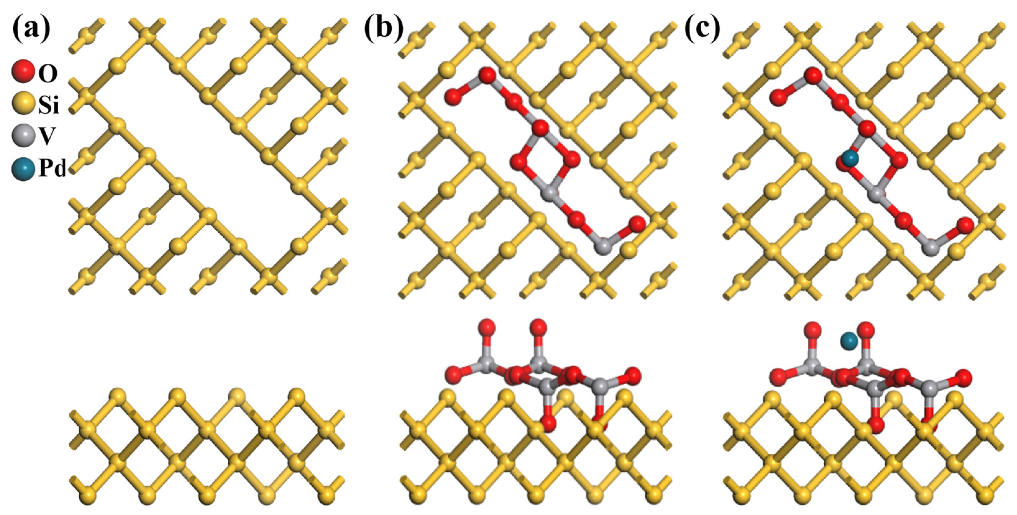
The atomic models in
Figure 4a–c depict the structural evolution from pristine PSi to PSi/V
2O
5 and Pd-PSi/V
2O
5. To construct the PSi framework (
Figure 4a), we initiated the simulation with a bulk crystalline silicon structure and introduced controlled pore architecture, with pore dimensions calibrated against experimental data. The simulated pore diameter represents a single pore for computational tractability, whereas experimental SEM (
Figure 5a) shows an average pore size of 75 ± 15 nm across a macroporous matrix, as confirmed by statistical analysis of 50 pores via ImageJ 1.53. In the PSi/V
2O
5 structure (
Figure 4b), the V
2O
5 framework retains its original arrangement, whereas in the Pd-decorated structure (
Figure 4c), a Pd atom is embedded within theV
2O
5 layer, causing localized distortions. From the top view, the Pd atom disrupts the coordination of adjacent oxygen atoms. The side view further emphasizes this interaction, revealing the Pd atom forming bonds with oxygen atoms within the V
2O
5 network. This structural modification suggests that Pd decoration alters the electronic properties and enhances the catalytic performance of the material.
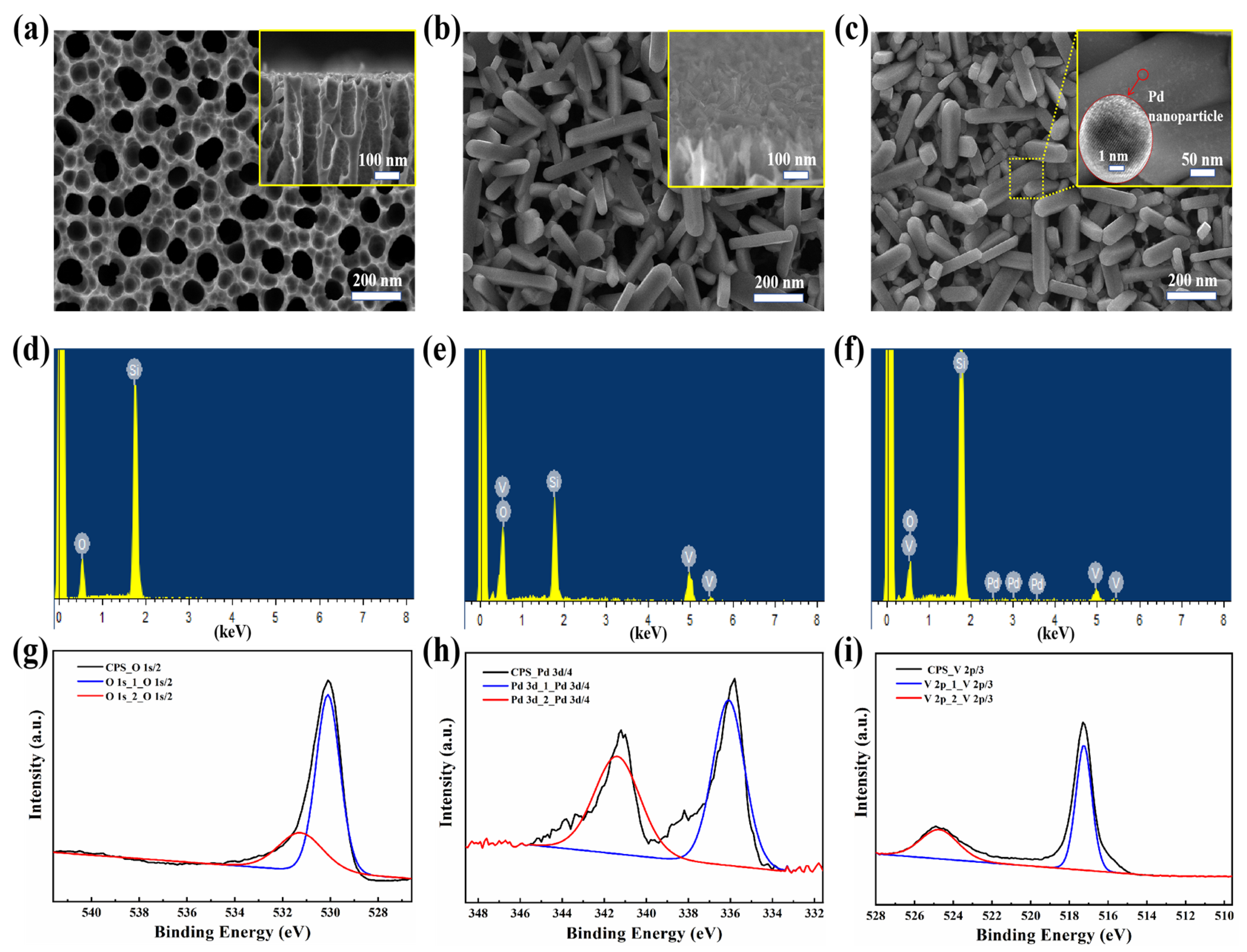
As shown in
Figure 5a, the SEM image of the bare PSi substrate demonstrated smooth pore walls with uniform spatial distribution, exhibiting an average pore diameter of 75 ± 15 nm. The higher-magnification inset image further confirmed the vertically aligned pore channels, consistent with the anisotropic etching mechanism described in
Section 2.1. SEM observations in
Figure 5b revealed that the V
2O
5 nanorobs formed a homogeneous and continuous coating on the PSi substrate surface at specific angles, with the majority of V
2O
5 nanorobs preferentially growing on the PSi surface rather than within the holes. The inset of
Figure 5b provides a cross-sectional view, further illustrating the uniform distribution of V
2O
5 nanorobs, which exhibit a width of 50–100 nm and a length of 200–400 nm. This configuration significantly increased the contact area between NO
2 molecules and both the V
2O
5 nanorobs and PSi. As shown in
Figure 5c, subsequent decoration with Pd nanoparticles via magnetron sputtering yielded uniform dispersion across the V
2O
5 nanorobs surface without observable aggregation, with Pd nanoparticles having an average diameter of approximately 5 nm (inset of
Figure 5c). This resulted in a more compact and uniform surface morphology, enhancing the material’s gas sensing performance.
Figure 5d–f presents the EDS spectra of PSi, PSi/V
2O
5, and Pd-PSi/V
2O
5. The Si element originates from PSi, the O and V elements are derived from the V
2O
5 nanorobs, and the Pd element comes from the Pd nanoparticles.
To further confirm the chemical composition and oxidation states of the Pd-V
2O
5/PSi composite, X-ray photoelectron spectroscopy (XPS) analysis was performed, and the results are presented in
Figure 5g–i. The XPS spectra reveal distinct peaks corresponding to O 1s, Pd 3d, and V 2p core levels. The O 1s spectrum shows two primary peaks at 530.1 eV (lattice oxygen, O
2−) and 531.3 eV (surface-adsorbed oxygen species, O
−), confirming the presence of reactive oxygen species critical for gas sensing. The Pd 3d spectrum exhibits peaks at 336.1 eV (Pd 3d
5/2) and 341.4 eV (Pd 3d
3/2), corresponding to metallic Pd
0. The V 2p spectrum shows peaks at 517.2 eV (V 2p
3/2) and 524.5 eV (V 2p
1/2), corresponding to the V
5+ oxidation state in V
2O
5, confirming the phase purity of the material. The combination of SEM, EDS, and XPS analyses provides comprehensive evidence for the structural, morphological, and chemical properties of the Pd-V
2O
5/PSi composite, supporting its enhanced gas sensing performance.
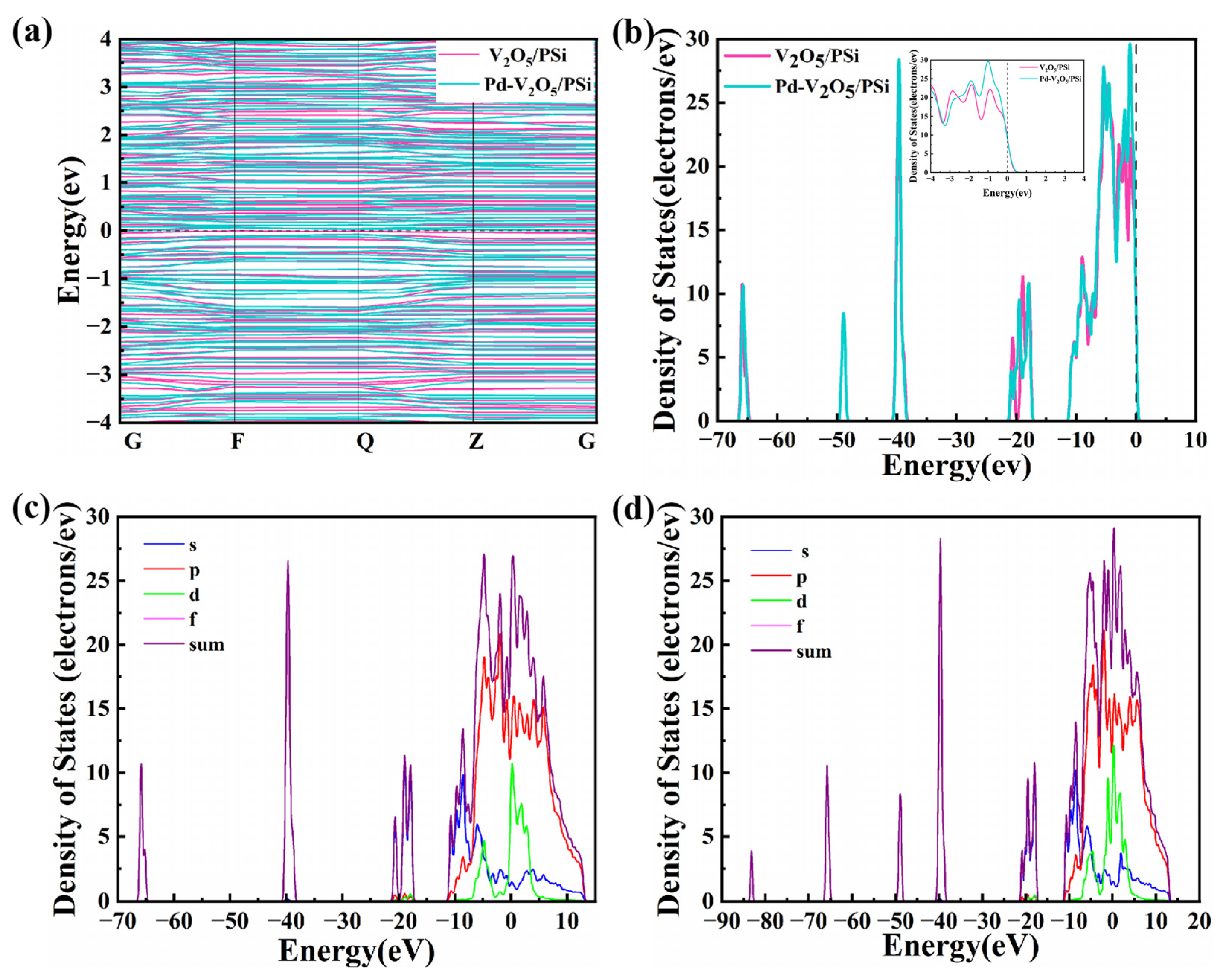
3.2. Electronic Properties and Band Structure Analysis
Figure 6a,b present the energy band structure and density of states (DOS) of V
2O
5/PSi before and after Pd decoration, respectively. In
Figure 6a, the band structure of V
2O
5/PSi exhibits a distinct bandgap, confirming its typical semiconducting behavior. The clear separation between the conduction band (CB) and valence band (VB) highlights limiting electronic transitions and resulting in relatively low conductivity. In contrast, Pd-V
2O
5/PSi demonstrates a reduced bandgap and the introduction of localized electronic states near the CB and within the bandgap. The DOS plot in
Figure 6b shows a notable increase in states near the Fermi level, attributed to the decoration of Pd, thereby enhancing electron transport properties, making the Pd-V
2O
5/PSi system more suitable for applications such as catalysis and gas sensing. The projected density of states (PDOS) analysis in
Figure 6c,d reveal distinct orbital contributions between the V
2O
5/PSi system (
Figure 6c) and Pd-V
2O
5/PSi system (
Figure 6d). In the V
2O
5/PSi system, the p-orbital exhibits hybridization near the Fermi level (0 eV), with contribution extending from −20 to +15 eV. The d-orbital of V
2O
5 contributes primarily between −20 and −10 eV, modulating interfacial charge transfer. Upon Pd decorating (
Figure 6d), the p-orbital shows intensified hybridization near the Fermi level, indicating strengthened O–Si–V
2O
5 interactions. Most notably, the d-orbital density surges at 0 eV, attributed to Pd d-states, which directly facilitates electron transfer at the Pd-V
2O
5 interface. These coordinated enhancements in s/p/d-orbital densities, particularly the Pd-induced d-state prominence near the conduction band, collectively optimize charge transport kinetics and catalytic activity.
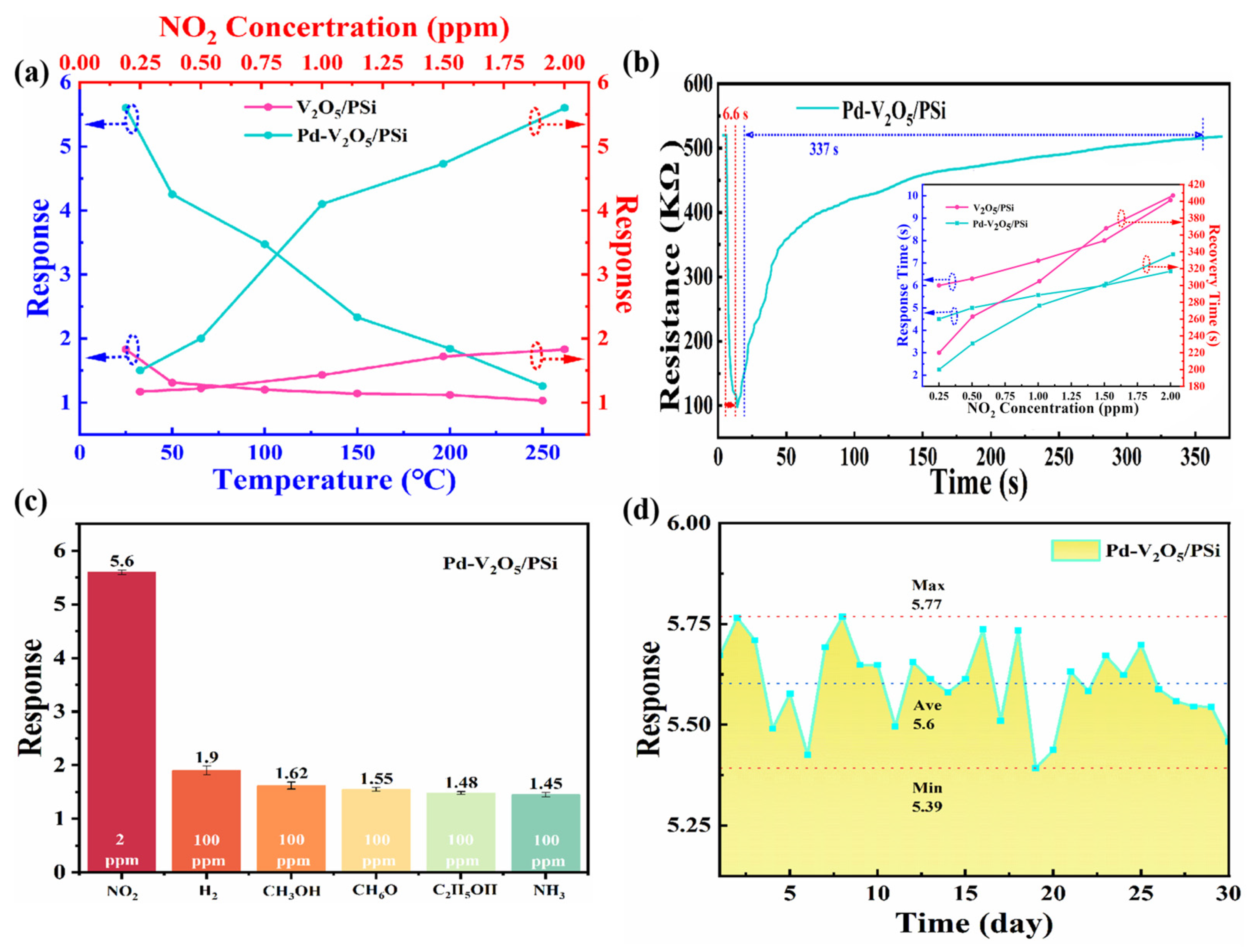
3.3. Gas-Sensing Performance
Figure 7 presents a comprehensive evaluation of the sensing performance of V
2O
5/PSi and Pd-V
2O
5/PSi composites. As shown in
Figure 7a, the temperature-dependent response characteristics of both composites were systematically investigated. The temperature sweep was performed at a fixed NO
2 concentration of 2 ppm to ensure unambiguous interpretation of thermal effects. The sensor responses of both V
2O
5/PSi and Pd-V
2O
5/PSi exhibited a decreasing trend with increasing temperature from 25 °C to 250 °C, suggesting that room temperature (25 °C) represents the optimal operating condition for these sensors. This behavior can be attributed to several factors: (1) at higher temperatures, the thermal energy of NO
2 molecules increases, leading to faster desorption from the sensor surface and reducing the extent of surface reactions; (2) the intrinsic carrier concentration in V
2O
5 increases with temperature, elevating the baseline conductivity and diminishing the relative resistance change; (3) the adsorption of oxygen species becomes less favorable at elevated temperatures, reducing the availability of pre-adsorbed oxygen ions critical for surface reactions; and (4) the catalytic efficiency of Pd nanoparticles may decrease at higher temperatures due to partial sintering or agglomeration. At this optimized temperature (25 °C), the concentration-dependent response was further examined across a range of NO
2 concentrations (0.25–2 ppm). Both composites demonstrated increasing response signals with elevated NO
2 concentrations. Specifically, the V
2O
5/PSi composite exhibited responses of 1.17, 1.22, 1.43, 1.72, and 1.83 for NO
2 concentrations of 0.25, 0.5, 1, 1.5, and 2 ppm, respectively. In contrast, the Pd-V
2O
5/PSi composite showed significantly enhanced responses of 1.5, 2, 4.1, 4.73, and 5.6 for the same NO
2 concentrations. Notably, at 2 ppm NO
2, the response of Pd-V
2O
5/PSi reached 5.6, which is 3.1 times higher than that of the undecorated V
2O
5/PSi (1.83). This substantial improvement in sensitivity, particularly at lower concentrations, highlights the effectiveness of Pd decoration in enhancing the sensing performance of the composite material.
The dynamic response characteristics, particularly response and recovery times, were thoroughly investigated as shown in
Figure 7b. From the dynamic response curve of Pd-V
2O
5/PSi to 2 ppm NO
2 at 25 °C, it can be observed that the resistance decreases upon exposure to NO
2, and after the response and recovery process, the resistance returns to its initial value. This behavior confirms the reversible nature of the sensing mechanism and the stability of the Pd-V
2O
5/PSi composite. The original response and recovery times for V
2O
5/PSi and Pd-V
2O
5/PSi to NO
2 concentrations (0.25–2 ppm) at 25 °C are included as an inset. The Pd-V
2O
5/PSi composite demonstrated superior performance, exhibiting both faster response rates and shorter recovery times compared to the V
2O
5/PSi. Specifically, the response/recovery times of Pd-V
2O
5/PSi for NO
2 concentrations of 0.25, 0.5, 1, 1.5, and 2 ppm were 4.5/200 s, 5.0/231 s, 5.5/276 s, 6.0/302 s, and 6.6/337 s, respectively. In contrast, the V
2O
5/PSi composite exhibited longer response/recovery times of 6.0/220 s, 6.3/263 s, 7.1/305 s, 8.0/368 s, and 9.8/407 s for the same NO
2 concentrations. This significant improvement in response and recovery kinetics highlights the enhanced performance of the Pd-decorated composite. The enhancement can be attributed to the catalytic effect of Pd nanoparticles, which facilitate the adsorption and surface reaction kinetics of NO
2 molecules on the V
2O
5 surface, leading to faster and more efficient gas sensing. Additionally, the porous structure of PSi provides abundant adsorption sites and optimized gas diffusion pathways, while the Pd-V
2O
5 heterojunction promotes efficient charge transfer and stabilizes the hole accumulation layer, further enhancing the sensing performance. In
Table 1, we can see that in low concentration detection, Pd-V
2O
5/PSi exhibited better gas sensing performance than most of the previously reported composites.
Selectivity, a crucial parameter for practical sensor applications, was systematically evaluated as presented in
Figure 7c. The gas sensing performance was tested against various interfering gases (H
2, CH
3OH, C
3H
6O, C
2H
5OH, NH
3) at a concentration of 100 ppm, significantly higher than the target NO
2 concentration (2 ppm). The results revealed that the Pd-V
2O
5/PSi composite maintained excellent selectivity towards NO
2, with response values of 1.9, 1.62, 1.55, 1.48, and 1.45 for H
2, CH
3OH, C
3H
6O, C
2H
5OH, and NH
3, respectively. In contrast, the response to 2 ppm NO
2 was significantly higher at 5.6, demonstrating minimal cross-sensitivity to other gases. This remarkable selectivity, combined with the enhanced sensitivity and improved response kinetics, underscores the effectiveness of Pd nanoparticle decoration in optimizing the NO
2 sensing properties of V
2O
5/PSi composites.
The long-term stability of the Pd-V
2O
5/PSi composite, as shown in
Figure 7d, was evaluated by exposing it to 2 ppm NO
2 over a 30-day period. The sensor exhibited highly consistent performance throughout the testing duration, with a maximum response of 5.77, a minimum response of 5.39, and an average response of 5.6. The response fluctuation remained within a narrow range of ±3.75%, demonstrating excellent stability and reliability. The stability is further enhanced by the robust structure of the PSi substrate and the strong interfacial interactions between Pd, V
2O
5, and PSi, which prevent degradation of the sensing material over time.
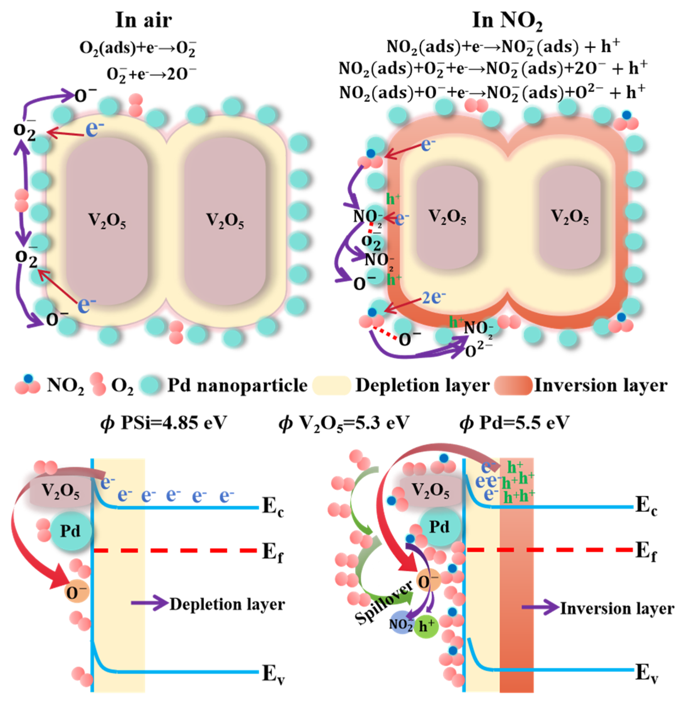
3.4. Mechanism of Gas-Sensing
V
2O
5, as a typical n-type MOS, initially follows the well-established depletion model for its NO
2 sensing mechanism. However, the introduction of Pd decoration and the formation of the V
2O
5/PSi heterojunction induce a transition to p-type behavior under NO
2 exposure, as confirmed by resistance dynamics. When exposed to ambient air, oxygen molecules chemisorb onto the surface of V
2O
5 nanorobs and are subsequently transformed into reactive oxygen species (O
2−, O
−, and O
2−) by capturing electrons from the conduction band of V
2O
5. This process forms an electron depletion layer near the surface of the V
2O
5 nanorobs, as described by the following reactions [
32]:
The NO
2-sensing mechanism of the Pd-V
2O
5/PSi composite is governed by hole-dominated conduction, as evidenced by the observed resistance decrease under NO
2 exposure. When exposed to NO
2, the molecules preferentially adsorb onto the V
2O
5/PSi surface due to their significantly higher electron affinity compared to oxygen molecules [
30]. This preferential adsorption occurs under dynamic adsorption–desorption equilibrium conditions [
31,
32,
33], where NO
2 molecules effectively compete with oxygen for surface active sites. The adsorption process extracts electrons from the valence band of V
2O
5, resulting in two significant phenomena: the expansion of the hole accumulation layer and the formation of an inversion layer where holes become the dominant charge carriers. Additionally, NO
2 molecules interact with pre-chemisorbed oxygen ions, facilitating further electron trapping, as described by the following reactions:
The presence of a hole accumulation layer in the Pd-V2O5/PSi heterostructure enhances its capability to adsorb oxidizing gases, particularly NO2. This enhancement is attributed to the increased number of adsorption sites created by the heterojunctions, which significantly contributes to the improved sensor performance. From the perspective of MOS gas sensor operation principles, specific surface area plays a crucial role in determining gas sensing performance. The V2O5/PSi heterostructure exhibits a high specific surface area, providing abundant active sites for gas molecule adsorption. This structural characteristic enables increased NO2 molecule adsorption on the material surface, enhanced electron transfer, and further widening of the depletion region. These combined effects result in a higher sensitivity and response to NO2 detection.
Based on the sensing mechanism of Pd-V
2O
5/PSi, the improved sensing characteristics can be attributed to three primary mechanisms, as illustrated in
Figure 8, which depicts the gas-sensing mechanism of Pd-V
2O
5/PSi in air and NO
2 environments. Firstly, the PSi substrate plays a crucial role in the NO
2 sensing process. The high specific surface area and excellent adsorption properties of PSi provide abundant diffusion pathways and adsorption sites for NO
2 gas molecules. This porous architecture facilitates both the penetration of NO
2 molecules into the composite material and their subsequent interaction with V
2O
5. Moreover, the porous structure enables rapid diffusion and desorption of gas molecules, thereby enhancing the response speed and recovery capability. Secondly, the formation of a Schottky junction at the Pd-V
2O
5 interface significantly contributes to the enhanced sensing performance. The work function difference between Pd (~5.5 eV) and n-V
2O
5 (~5.3 eV) induces electron transfer from V
2O
5 to Pd until Fermi level alignment is achieved. This process creates a hole accumulation layer at the Pd-V
2O
5 interface, which stabilizes the inversion layer and enhances hole conduction under NO
2 exposure. The metal spillover effect generates additional active adsorption sites on Pd nanoparticles, facilitating enhanced gas molecule adsorption [
20]. The increased concentration of adsorbed species enables NO
2 molecules to not only directly capture electrons from the V
2O
5 conduction band but also react with the pre-adsorbed oxygen ions, leading to enhanced sensing response, as evidenced by the results shown in
Figure 7a. Thirdly, the catalytic properties of Pd nanoparticles play a significant role in improving sensor performance. Pd nanoparticles reduce the activation energy for chemical adsorption of gas molecules and accelerate the rate of chemical reactions. This catalytic effect lowers the optimal operating temperature of the Pd-V
2O
5/PSi while simultaneously reducing response and recovery times. The enhanced coverage of oxygen ions on the sensor surface contributes to the improved NO
2 sensing capability. Furthermore, Pd nanoparticles facilitate the adsorption/desorption of NO
2, molecule–ion conversion of oxygen, and the interaction between NO
2 and chemisorbed oxygen ions, resulting in significantly improved response and recovery characteristics. The synergistic combination of these mechanisms enables the Pd-V
2O
5/PSi to achieve superior response characteristics and shorter response/recovery times at room temperature compared to the undecorated V
2O
5/PSi.
3.5. Role of Pd Decoration in Enhancing Sensing Performance
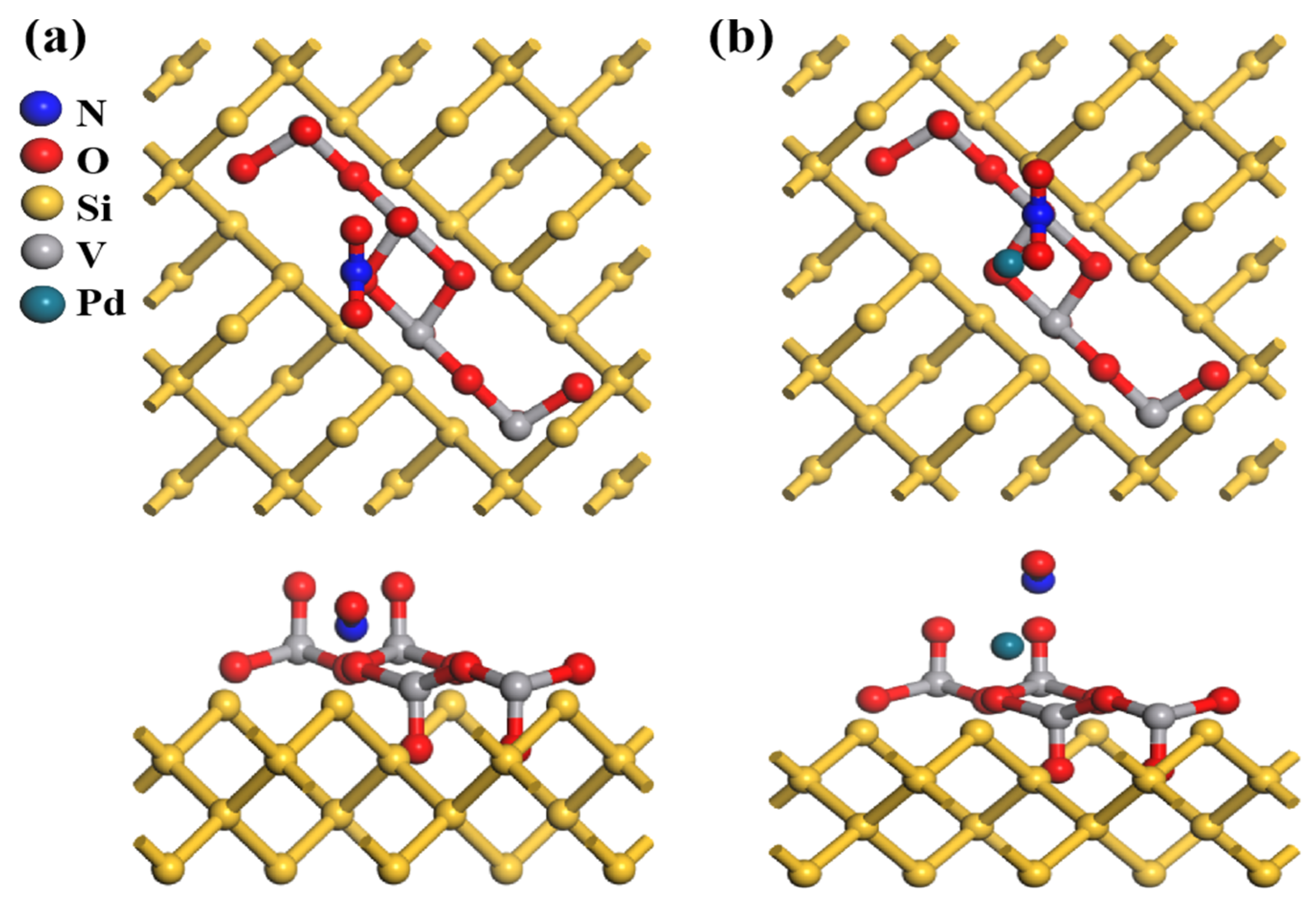
In the atomic models shown in
Figure 9a,b, the undecorated V
2O
5/PSi system in
Figure 9a shows NO
2 adsorption primarily on the oxygen atoms of the V
2O
5 framework, forming stable but weak bonds with minimal structural changes. In contrast, the Pd-V
2O
5/PSi system in
Figure 9b exhibits stronger NO
2–surface interactions, with Pd atoms serving as additional adsorption sites that facilitate electron transfer and enhance adsorption capacity. This modification strengthens NO
2 adsorption by altering the local bonding environment and increasing surface reactivity, suggesting improved electronic and catalytic performance.
The experimental results (
Figure 7) demonstrate that the decoration of Pd nanoparticles significantly enhances the gas sensing performance of the V
2O
5/PSi composite. As shown in the dynamic response curve of Pd-V
2O
5/PSi to 2 ppm NO
2 at 25 °C (
Figure 7b), the resistance decreases upon exposure to NO
2, and after the response and recovery process, the resistance returns to its initial value. This behavior confirms the reversible nature of the sensing mechanism and the stability of the Pd-V
2O
5/PSi composite.
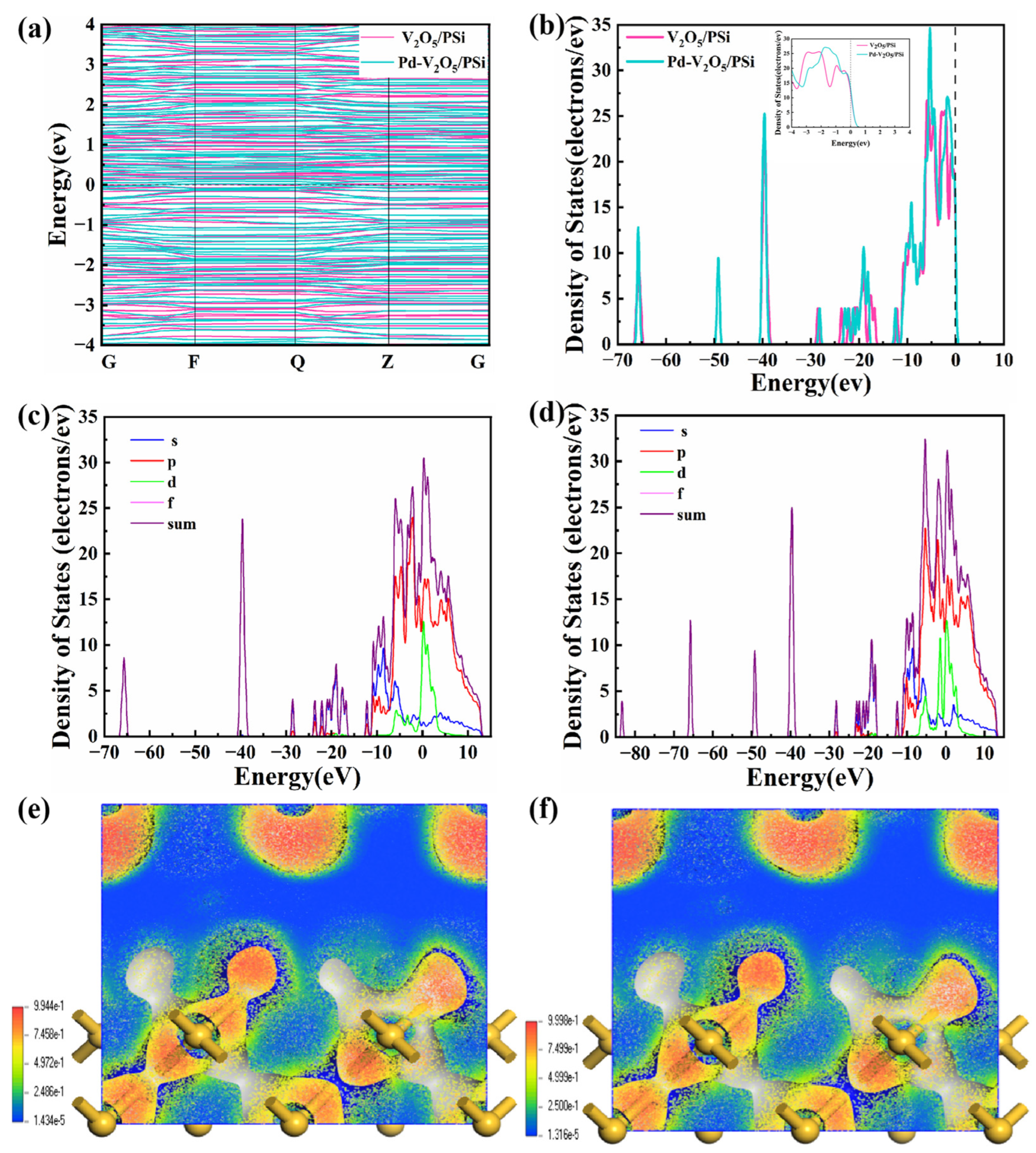
Figure 10a–f presents a comprehensive analysis of the structural, electronic, and adsorption properties of V
2O
5/PSi and Pd-V
2O
5/PSi composites in an NO
2 environment, further elucidating these effects.
In
Figure 10a, the NO
2 adsorption of the V
2O
5/PSi system induces minimal changes, reflecting weak adsorption and limited electronic coupling. In contrast, the Pd-V
2O
5/PSi system exhibits a reduced bandgap and localized electronic states near the Fermi level, enhancing conductivity. Pd decoration introduces additional energy levels near the CB and increases DOS peaks (
Figure 10b), indicating stronger electronic coupling and enhanced electron density. These changes improve NO
2 adsorption and reactivity, highlighting Pd’s role as an electronic coupling bridge.
The PDOS analysis of NO
2-adsorbed systems reveals critical electronic modifications induced by Pd decoration. In the PSi-V
2O
5/NO
2 system (
Figure 10c), the s-orbital dominates at mid-to-low energies (−30 to +15 eV), reflecting Si–O–V
2O
5 interfacial interactions. The p-orbital hybridizes strongly near the Fermi level (0 eV) and spans −10 to +5 eV, facilitating charge transfer. The d-orbital contributes broadly (−20 to +10 eV), primarily from V
2O
5’s transition metal centers. Upon Pd decoration (
Figure 10d), the p-orbital exhibits intensified hybridization near the Fermi level, amplifying oxygen-mediated charge delocalization. Most critically, the d-orbital develops a prominent peak at 0 eV, attributed to Pd 4d states, which directly bridges the CB and NO
2 antibonding orbitals. The enhanced Pd 4d contribution correlates with the experimentally observed 3.1-fold improvement in sensor response (
Section 3.3), demonstrating that Pd decoration facilitates interfacial charge dynamics rather than altering the bulk band structure. These findings are consistent with the improved sensitivity and selectivity observed in
Section 3.3, where Pd-V
2O
5/PSi exhibited faster response and recovery times compared to the undecorated V
2O
5/PSi composite.
The ELF shown in
Figure 10e,f provides further insights. In
Figure 10e, the V
2O
5/PSi system shows localized electron density primarily in specific regions of the material surface, where yellow and red regions represent higher electron density, while blue areas indicate lower electron density. The color distribution highlights the regions where the composite surface interacts most strongly with NO
2 molecules. The range of electron density values, from 1.434 × 10
−5 to 9.944 × 10
−1, further emphasizes localized electronic behavior near the surface, suggesting that the V
2O
5/PSi composite exhibits strong surface interactions with the gas molecules. In contrast, the Pd-V
2O
5/PSi system in
Figure 10f exhibits a more extensive electron density in the yellow and red regions, indicating an increase in overall electron localization. The range of electron density values from 1.316 × 10
−5 to 9.998 × 10
−1 highlights a more concentrated electron distribution, especially at the Pd sites and the adjacent material surface. This enhanced electron localization suggests that Pd decoration not only increases the material’s interaction with gas molecules but also improves its electron transfer capability, as evidenced by the improved sensing performance in
Section 3.3. As a result, the Pd-V
2O
5/PSi composite demonstrates stronger interactions between Pd and NO
2, significantly improving the material’s electronic properties, sensitivity, and selectivity to NO
2.
Collectively, these results reveal that Pd decoration markedly enhances the electronic structure, adsorption capacity, and reactivity of the V
2O
5/PSi composite. The introduction of localized states, reduced bandgap, increased DOS peaks, and enhanced electron localization facilitate efficient electron transfer and stabilize NO
2 interactions. These findings are consistent with the experimental results in
Section 3.3, where Pd-V
2O
5/PSi exhibited superior sensing performance, including faster response/recovery times and higher sensitivity to NO
2, underscoring its potential for advanced gas sensing and catalytic applications by leveraging its improved conductivity and reactivity.


