Abstract
The electronic states in flat bands possess zero group velocity and null charge mobility. Recently, flat electronic bands with fully localized states have been predicted in nanowires, when their hopping integrals between first, second, and third neighbors satisfy determined relationships. Experimentally, these relationships can only be closely achieved under external pressures. In this article, we study the alternating current (AC) in such nanowires having nearly flat electronic bands by means of a new independent channel method developed for the Kubo–Greenwood formula including hopping integrals up to third neighbors. The results reveal a large AC conductivity sensitive to the boundary conditions of measurement, where the charge carriers resonate with the external electric field by oscillating around their localized positions.
1. Introduction
In a flat electronic band, constituted by a huge number of compactly localized states resulting from the destructive interference, the charge carriers have an infinite effective mass and nil group velocity, which lead to a quenched kinetic energy and a zero conduc-ivity of direct current (DC). This highly degenerate energy level becomes a perfect platform to enhance strongly correlated electronic phenomena, such as the magic-angle-induced superconductivity observed in twisted bilayer graphene [1]. In the last decade, flat photonic bands have also been extensively studied, where unconventional light localization [2] and slow light propagation [3] are observed in engineered photonic lattices [4]. However, the alternating current (AC) in flat and nearly flat bands under low-frequency oscillating electric field is an important but less studied topic, in spite of the recent review of the universality of AC conduction in disordered solids [5] and a detailed study of electric conductivity at the zero-frequency limit in flat bands of the Su–Schrieffer–Heger model and Lieb lattice using two variations of the Kubo–Greenwood formula [6].
On the experimental side, the observation of flat bands requires fine-tuning around the critical conditions predicted by the theory, which have been nearly achieved leading to almost flat or extremely narrow bands [7]. In addition, nanowires with two-dimensional quantum confinement are currently performing a crucial building-block role in nanoelectronics [8]. In this article, we report a real-space tight-binding study of the AC conductivity carried out in cubically structured nanowires with nearly flat bands. A new independent channel method was developed for the Kubo–Greenwood formula including the first, second, and third neighbor hopping interactions, whose details can be found in Appendix A. This method combined with the previously developed real-space renormalization technique [9] allows an accurate calculation of the AC conductivity in mentioned nanowires of macroscopic length containing multiple structural interfaces commonly present in the AC measurement setup. When the flat-band or destructive-interference condition is closely satisfied, we observe the formation of several extremely narrow bands derived from the truly flat one, as well as an exceptionally high resonant AC conductivity at very low frequencies. These AC resonant peaks of a nanowire under external pressure can be used for the pressure measurement utilizing a simple electric circuit, instead of the widely used ruby fluorescence spectrum for pressure determination [10], since the external pressure modifies the electronic band width through hopping integrals and then the frequency of these resonant peaks.
2. Real Space Modeling
For the study of electronic transport in flat bands of a cubically structured nanowire, as well as the influence of AC measurement setup, we have chosen the real-space approach by means of a tight-binding model including hopping integrals between first (), second (), and third () neighboring atoms, whose Hamiltonian (A6) through a unitary transformation can be rewritten as a sum (A17) of those obtained from each independent channel, as discussed in Appendix A and schematically represented in Figure 1.
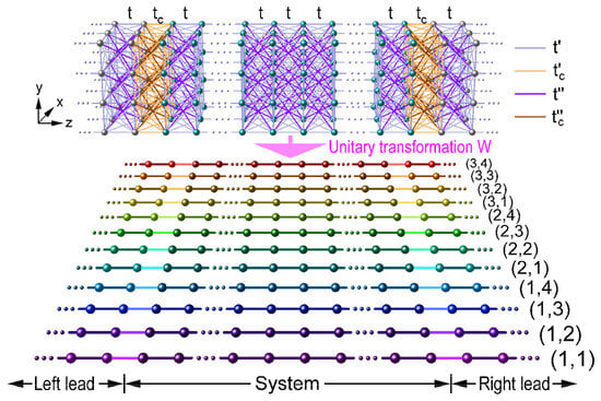
Figure 1.
By means of a unitary transformation, a cubically structured nanowire with cross section of 3 × 4 atoms and hopping interactions up to third neighbors through , and is represented by 12 independent channels indexed by , where the system and its leads are connected by the hopping integrals and originated from their structural interfaces.
The Hamiltonian of channel along the Z-directional can be expressed as
where k counts each atom of the channel, is the on-site energy and is the nearest-neighbor hopping integral with , , and defined in (A12).
The channel becomes to a fully disconnected chain with a highly degenerate flat band at energy equal to , if its hopping integrals became to zero, i.e.,
In other words, conditions for the flat-band appearance are
for a nanowire containing atoms.
For example, let us consider a narrow nanowire of atoms, which has a flat band at , if in Equation (3), i.e., and . On the other hand, if and or in Equation (3), where is the golden ratio, the flat band would be located at . In the first case of , the degeneracy of flat band is , while it is when , where is the number of atoms along the Z direction of nanowire.
In Figure 2, the band width of each independent channel described by Hamiltonian (1) is plotted as a function of the ratio of hopping integrals for a nanowire of atoms, which is connected at its ends to two semi-infinite periodic leads with the same cross section and Hamiltonian parameters of the system. Observe that channel (3,4), shown in Figure 2m, possesses two flat bands located at and . In contrast, channels (1,4) and (2,4) hold a single flat band at , while channels (3,1), (3,2), and (3,3) own the another at .
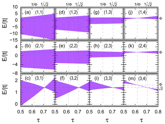
Figure 2.
(a–m) Band width of independent channels , numbered in each figure, versus the hopping integral ratio for a nanowire with cross section of atoms, being .
On the other hand, the electronic density of states (DOS) can be calculated by means of the Green’s function determined by Hamiltonian (A6) as [11]
Using Equation (A30) in Appendix A, the DOS could be rewritten as
where
is the one-dimensional DOS of channel , which is efficiently calculated in this work by means of a real-space renormalization method given in Appendix A of ref. [9].
Figure 3a shows the DOS in logarithmic scale as a function of the energy (E) for the same nanowire of Figure 2 with a hopping integral ratio (blue line) and (red line), where an imaginary part of energy is used. Figure 3b presents a magnification of Figure 3a around , where the DOS of channels (3,1) (magenta line), (3,2) (orange line), (3,3) (green line), and (3,4) (cyan line) using are also plotted.
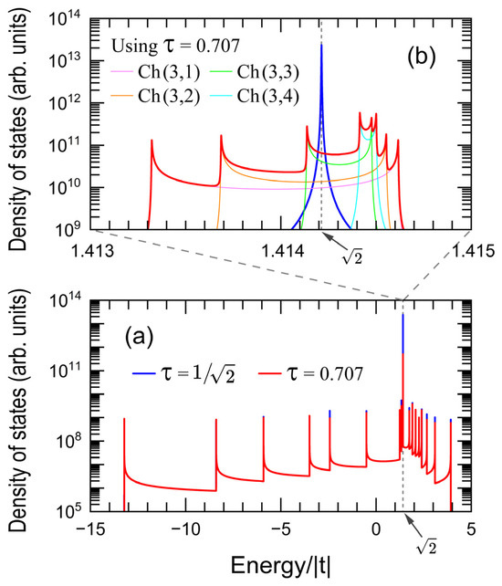
Figure 3.
(a) Electronic density of states (DOS) versus energy with for the same nanowire of Figure 2 with (blue line) and (red line). (b) Magnification of DOS around including those of channels (3,1) (magenta line), (3,2) (orange line), (3,3) (green line) and (3,4) (cyan line) for .
Notice in Figure 3a the nearly flat band (red line) with possessing a DOS two orders of magnitude lower than that of the true one (blue line) at obtained from . Additionally, this almost flat band has a sophisticate band structure originated from the asymmetrical band broadening in channels (3,1), (3,2), (3,3) and (3,4) when , as shown in Figure 3b, which may also be noted by comparing Figure 2c,f,i,m.
3. AC Conductivity
Within the linear response theory, the electrical conductivity (σ) can be calculated by means of the Kubo–Greenwood formula presented in Equation (A3), which could be analytically evaluated at zero temperature, for a periodic chain of N atoms connected to two semi-infinite periodic leads with the same parameters of the chain, leading to [9]
and its corresponding DC conductivity is [12]
where is the Heaviside step function, ε is the on-site energy, t is the nearest neighbor hopping integral, and a is the interatomic distance in the periodic chain.
In Figure 4a, the AC electrical conductivity at obtained from Equations (A36) and (7) is plotted as a function of the chemical potential (μ) and the external electrical-field frequency (ω) for the same nanowire of Figure 3 with a hopping integral ratio . Notice the ballistic DC transport in each independent channel and the presence of nearly flat bands around , as well as a general decreasing behavior of σ with the frequency in the interval . Figure 4b further illustrates an amplification of the spectrum around using a logarithmic scale of frequency, where a ballistic DC conductivity is also observed in the four nearly flat bands, in contrast with the zero conductivity of truly flat bands when . However, such ballistic conductivity quickly vanishes when in parallel to its general disappearance in the rest bands starting from
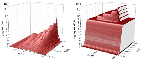
Figure 4.
(a) Zero-temperature electrical conductivity versus the chemical potential () and the frequency () for the same nanowire of Figure 3 with a hopping integral ratio and (b) its magnification around plotted in the logarithmic scale of frequency.
The general decline of electrical conductivity around can be noted from Equation (7), i.e., for an independent channel of atoms, when the chemical potential and , we have , which leads to an almost constant behavior of the conductivity, contrasted to the rapid decay with frequency, as much as , when . For the case of nearly flat bands, their hopping integral is about , and then, the AC conductivity of these narrow bands starts their rapid decay around .
Now, let us consider a more realistic measurement configuration of AC conductivity, where exist structural interfaces between the sample and metallic cables represented by periodic leads. These interfaces could be modeled by introducing new hopping integrals , and , respectively denoted by camel, beige, and brown lines in Figure 1, that connect the first, second, and third neighboring atoms at the interface between the nanowire and its two semi-infinite periodic leads. In Figure 5a,b, the AC conductivity spectra around obtained from the Kubo–Greenwood formula (A3) using a small enough imaginary part of [13] are presented for the nanowire of Figure 2 with the connecting hopping integral (b) and (c) , while Figure 5c shows an amplification of DOS versus the electronic energy (E) with an imaginary part of in a small interval of for the case of . It would be worth mentioning that all the numerical calculations presented in this article have been carried out in quadruple precision.

Figure 5.
(a,b) Zero-temperature electrical conductivity as a function of the chemical potential (μ) and frequency (ω) for the nanowire illustrated in Figure 1 with (a) and (b) . (c) Magnification of the density of states (DOS) as a function of energy (E) with around for the case .
Observe the appearance of sharp resonant peaks at low frequency in Figure 5a, when a slightly perturbated connecting hopping integral of is introduced, where the presence of destroys the translational symmetry producing discrete energy spectra, as illustrated in Figure 5c and then, the presence of resonant AC conduction peaks [14]. Moreover, close to the largest resonant peak, indicated by blue arrows, there are several smaller ones at higher frequencies originated from electronic transitions, for example, between the ground state and the third (green arrows) or fifth (orange arrows) excited ones, in contrast with the forbidden transitions between the ground state and the second or forth excited ones, due to that the odd or even symmetry of wavefunctions plays a decisive role in the Fermi golden rule applied to the electric dipolar induced electronic transitions [15]. This resonant AC transport is even enhanced when leading to maximal values of AC conductivity about times of the DC ballistic one (), as shown in Figure 5b. Observe also in Figure 5b the U-form location of AC resonant peaks in the μ-ω plane, which originated from the distribution of electronic states determined by the dispersion relation of finite periodic chains [16].
4. Conclusions
A new independent channel method for the Kubo–Greenwood formula, including hopping interactions between first, second, and third neighbors in cubically structured nanowires, is presented, which combined with the real-space renormalization method [9], permits a direct AC conductivity calculation of macroscopic length nanowires with multiple structural interfaces without additional approximations. Flat and nearly flat bands in such nanowires were analytically and numerically investigated, including their appearance conditions and the bandwidth of almost flat ones, where the destructive quantum interference conditions are strictly and approximately satisfied.
A narrow nanowire of atoms with a ratio of the second-neighbor hopping integral () to the first-neighbor one (t), , has been chosen as an example for the electronic transport study, where extremely high AC conductivity ( times of the DC ballistic conductivity) is observed at a very low frequency, less than one Hz if and . This resonant AC frequency sensitively depends on the value of τ and the system length, where the former determines the width of nearly flat bands, and the latter decides the distribution of electronic states in the energy scale.
In general, the flat band required a specific relationship between the first, second, and third hopping-integral strengths, which can be closely achieved by applying external pressures to the nanowire along X and Y directions, while the electronic band filling could be controlled via the application of a gate voltage. Despite the zero electronic mobility of flat bands, their charge carriers actually always oscillate around their localized positions, as suggested by the uncertainty principle of quantum mechanics. When these oscillations resonate with the frequency of the external electric field, a large AC response would be observed, as occurred in Figure 5b. As mentioned in the introduction section, these high resonant peaks can be used in the pressure measurement, since the experimental verification of nearly flat bands in nanowires is suggested to be carried out by applying hydrostatic external pressure to the cross-section of nanowires to achieve the flat-band appearance condition and the frequency of these resonant peaks is sensitive to the bandwidth through the ratio of hopping integrals.
Finally, it would be worth mentioning that the electron–electron and electron–phonon interactions are not explicitly included in the Hamiltonian of this study and their contributions within the mean-field approximation could be considered via hopping integrals depended on the electronic density and temperature. This extension of the study is currently being carried out. On the other hand, the combination of independent channel and real-space renormalization methods [17] presented in this article could be a useful tool in the design and study of aperiodic electronic and photonic devices containing multiple structural interfaces, like semiconductor diodes, bipolar junction and graphene transistors [18], as well as Fabry–Perot resonant cavities [19].
Author Contributions
Conceptualization, V.S. and C.W.; methodology, V.S. and C.W.; software, V.S. and C.W.; validation, V.S. and C.W.; formal analysis, V.S. and C.W.; investigation, V.S. and C.W.; resources, V.S. and C.W.; writing-original draft preparation, V.S. and C.W.; writing-review and editing, V.S. and C.W.; funding acquisition, V.S. and C.W. All authors have read and agreed to the published version of the manuscript.
Funding
This research has been partially supported by the Consejo Nacional de Humanidades, Ciencias y Tecnologías via grant CF-2023-I-830 and by the National Autonomous University of Mexico (UNAM) through projects PAPIIT-IN112522 and PAPIIT-IN110823. The computations were performed at Miztli of UNAM supported by LANCAD-UNAM-DGTIC-039 and LANCAD-UNAM-DGTIC-182.
Data Availability Statement
Data are contained within the article.
Acknowledgments
The technical assistance of Alejandro Pompa, Oscar Luna, Cain González, Silvia E. Frausto, and Yolanda Flores is fully appreciated.
Conflicts of Interest
The authors declare no conflicts of interest.
Appendix A. Independent Channel Method for the Kubo–Greenwood Formula
The electrical conductivity () of alternating current (AC) within the linear response approximation can be calculated by means of the Kubo–Greenwood formula given by [11],
where the factor 2 counts the possible electron spin orientations, Ω is the volume of system, is the projection of momentum operator along the Z direction or the external electric-field direction, and is the Fermi–Dirac distribution with chemical potential μ and temperature T. The retarded and advanced single-electron Green’s functions are, respectively defined as [11],
where η is the imaginary part of energy and is the eigenfunction of Hamiltonian satisfying the stationary Schrödinger equation . As , the Kubo–Greenwood formula (A1) can be rewritten in terms of the discontinuity as
whose trace could be expressed as [9]:
where , and using (A2) we have
with υ and or −.
For a cubically structured nanowire along the Z direction, containing atoms and transversal structural interfaces, the s-band tight-binding Hamiltonian of spinless electrons with null on-site energies and hopping integrals between first (), second and third neighbors is [20]
where
and
Respectively, describe the electron hopping between first, second, and third neighboring atoms. In Hamiltonians (A7), (A8), and (A9), l, j and k are integer numbers correspondingly counting atoms along the X, Y, and Z directions with wavefunctions in the Dirac notation as [21], being , and the one-dimensional (1D) Wannier functions. Hence, Hamiltonian (A6) can be rewritten as [22,23]
where symbol denotes the Kronecker product, , for , and being , and τ is a dimensionless parameter with , , and .
Now, we use the eigenstates of the nanowire’s cross-section on the XY plane to reduce Hamiltonian (A10) into a 1D effective one along the Z direction given by
where , , and [16],
In fact, Hamiltonian (A11) can be rewritten as
where is the on-site energy and is the nearest-neighbor hopping integral of a Z-directional chain, denoted as channel. In other words, the nanowire is transformed into a set of independent channels by means of a unitary transformation made of the eigenvectors of , i.e.,
where and are, respectively the diagonal version of matrices and . In Equation (A14), we have used the following identity
Hence, Hamiltonian (A10) is transformed as
with , , and Thus, given that , and , (A16) can be rewritten as
which is consistent with Equation (A11).
In general, the projection of momentum operator along the Z direction may be calculated via [9]
where with , being the Z-direction Cartesian coordinate of atom k. Applying the same unitary transformation to and using (A17), we obtain
since . Employing (A13) and (A15), Equation (A19) can be written as
where
and
In consequence, Equation (A20) converts to
where a uniform separation between atoms along Z direction, , is assumed. Hence,
with
On the other hand, the Green’s function is determined by the Dyson equation given by [11], , which by applying the unitary transformation and using (A17), we obtain
and then,
where .
Given that the density of states (DOS) is related to the Green’s function as [11]
using (A27), and , (A28) could be rewritten as
and then
where .
On the other hand, sum in (A5) can also be rewritten as
where the identities and are used. Hence, using (A24), (A27), and , Equation (A31) converts to
where . Given that, for example, , and , (A32) can be simplified to
which could be rewritten as
Therefore, (A4) might be expressed as a sum of traces of each channel , i.e.,
So, the Kubo–Greenwood formula (A3) in terms of independent channels can be written as
where
and , being and correspondingly the volumes of system in the parallel and perpendicular subspaces with respect to the external electric field.
References
- Cao, Y.; Fatemi, V.; Fang, S.; Watanabe, K.; Taniguchi, T.; Kaxiras, E.; Jarillo-Herrero, P. Unconventional superconductivity in magic-angle graphene superlattices. Nature 2018, 556, 43–50. [Google Scholar] [CrossRef] [PubMed]
- Tang, L.; Song, D.; Xia, S.; Xia, S.; Ma, J.; Yan, W.; Hu, Y.; Xu, J.; Leykam, D.; Chen, Z. Photonic flat-band lattices and unconventional light localization. Nanophotonics 2020, 9, 1161–1176. [Google Scholar] [CrossRef]
- Kumar, A.; Tan, Y.J.; Navaratna, N.; Gupta, M.; Pitchappa, P.; Singh, R. Slow light topological photonics with counter-propagating waves and its active control on a chip. Nat. Commun. 2024, 15, 926. [Google Scholar] [CrossRef]
- Yang, J.; Li, Y.; Yang, Y.; Xie, X.; Zhang, Z.; Yuan, J.; Cai, H.; Wang, D.-W.; Gao, F. Realization of all-band-flat photonic lattices. Nat. Commun. 2024, 15, 1484. [Google Scholar] [CrossRef] [PubMed]
- Dyre, J.C.; Schrøder, T.B. Universality of ac conduction in disordered solids. Rev. Mod. Phys. 2000, 72, 873–892. [Google Scholar] [CrossRef]
- Huhtinen, K.-E.; Törmä, P. Conductivity in flat bands from the Kubo-Greenwood formula. Phys. Rev. B 2023, 108, 155108. [Google Scholar] [CrossRef]
- Danieli, C.; Andreanov, A.; Leykam, D.; Flach, S. Flat band fine-tuning and its photonic applications. Nanophotonics 2024, 13, 3925–3944. [Google Scholar] [CrossRef]
- Jia, C.; Lin, Z.; Huang, Y.; Duan, X. Nanowire electronics: From nanoscale to macroscale. Chem. Rev. 2019, 119, 9074–9135. [Google Scholar] [CrossRef] [PubMed]
- Sánchez, V.; Wang, C. Application of renormalization and convolution methods to the Kubo-Greenwood formula in multidimensional Fibonacci systems. Phys. Rev. B 2004, 70, 144207. [Google Scholar] [CrossRef]
- Forman, R.A.; Piermarini, G.J.; Barnett, J.D.; Block, S. Pressure measurement made by the utilization of ruby sharp-line luminescense. Science 1972, 176, 284–285. [Google Scholar] [CrossRef] [PubMed]
- Economou, E.N. Green’s Functions in Quantum Physics, 3rd ed.; Springer: Berlin, Germany, 2006; pp. 14–16, 183–184. [Google Scholar]
- Oviedo-Roa, R.; Pérez, L.A.; Wang, C. AC conductivity of the transparent states in Fibonacci chains. Phys. Rev. B 2000, 62, 13805–13808. [Google Scholar] [CrossRef]
- Sánchez, V.; Wang, C. Resonant AC conducting spectra in quasiperiodic systems. Int. J. Comput. Mater. Sci. Eng. 2012, 1, 1250003. [Google Scholar] [CrossRef]
- Sánchez, V.; Wang, C. Improving the ballistic AC conductivity through quantum resonance in branched nanowires. Philos. Mag. 2015, 95, 326–333. [Google Scholar] [CrossRef]
- Griffiths, D.J.; Schroeter, D.F. Introduction to Quantum Mechanics, 3rd ed.; Cambridge University Press: Cambridge, UK, 2018; pp. 246–247. [Google Scholar]
- Sutton, A.P. Electronic Structure of Materials; Oxford University Press: New York, NY, USA, 1994; p. 41. [Google Scholar]
- Sánchez, V.; Wang, C. Real space theory for electron and phonon transport in aperiodic lattices via renormalization. Symmetry 2020, 12, 430. [Google Scholar] [CrossRef]
- Sánchez, F.; Sánchez, V.; Wang, C. Independent dual-channel approach to mesoscopic graphene transistors. Nanomaterials 2022, 12, 3223. [Google Scholar] [CrossRef] [PubMed]
- Palavicini, A.; Wang, C. Ab initio design and experimental confirmation of Fabry-Perot cavities based on freestanding porous silicon multilayers. J. Mater. Sci. Mater. Electron. 2020, 31, 60–64. [Google Scholar] [CrossRef]
- Sánchez, V.; Wang, C. A real-space study of flat bands in nanowires. Nanomaterials 2023, 13, 2864. [Google Scholar] [CrossRef] [PubMed]
- Bruus, H.; Flensberg, K. Many-Body Quantum Theory in Condensed Matter Physics, an Introduction; Oxford University Press: Oxford, UK, 2016; pp. 3–9. [Google Scholar]
- Sire, C. Electronic spectrum of a 2D quasi-crystal related to the octagonal quasi-periodic tiling. Europhys. Lett. 1989, 10, 483–488. [Google Scholar] [CrossRef]
- Sánchez, F.; Sánchez, V.; Wang, C. Ballistic transport in aperiodic Labyrinth tiling proven through a new convolution theorem. Eur. Phys. J. B 2018, 91, 132. [Google Scholar] [CrossRef]
Disclaimer/Publisher’s Note: The statements, opinions and data contained in all publications are solely those of the individual author(s) and contributor(s) and not of MDPI and/or the editor(s). MDPI and/or the editor(s) disclaim responsibility for any injury to people or property resulting from any ideas, methods, instructions or products referred to in the content. |
© 2024 by the authors. Licensee MDPI, Basel, Switzerland. This article is an open access article distributed under the terms and conditions of the Creative Commons Attribution (CC BY) license (https://creativecommons.org/licenses/by/4.0/).