
Progress and Challenges of Three-Dimensional/Two-Dimensional Bilayered Perovskite Solar Cells: A Critical Review


Abstract
1. Introduction
2. Organic Precursors
3. Alkylammonium Precursors
4. Arylammonium Precursors
5. Other Organic Precursors
6. Effects on Efficiency
6.1. Reduced Charge Recombination
6.2. Energy Level Alignment
6.3. Reduced Ion Movement
7. Effect on Stability
7.1. Humidity Stability
7.2. Thermal Stability
8. Challenges
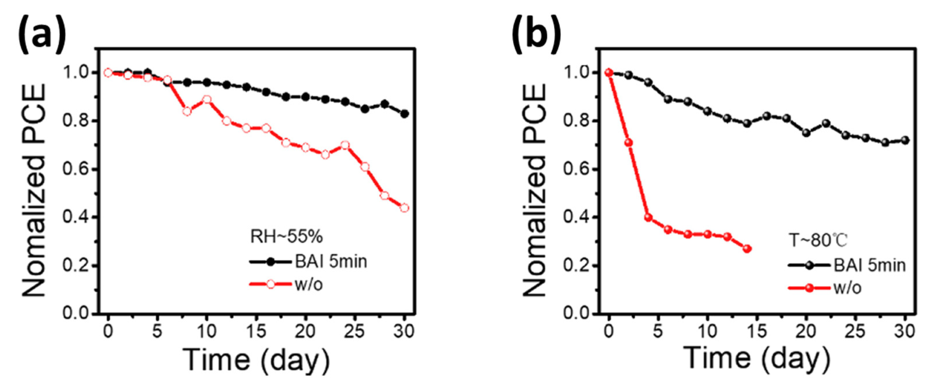
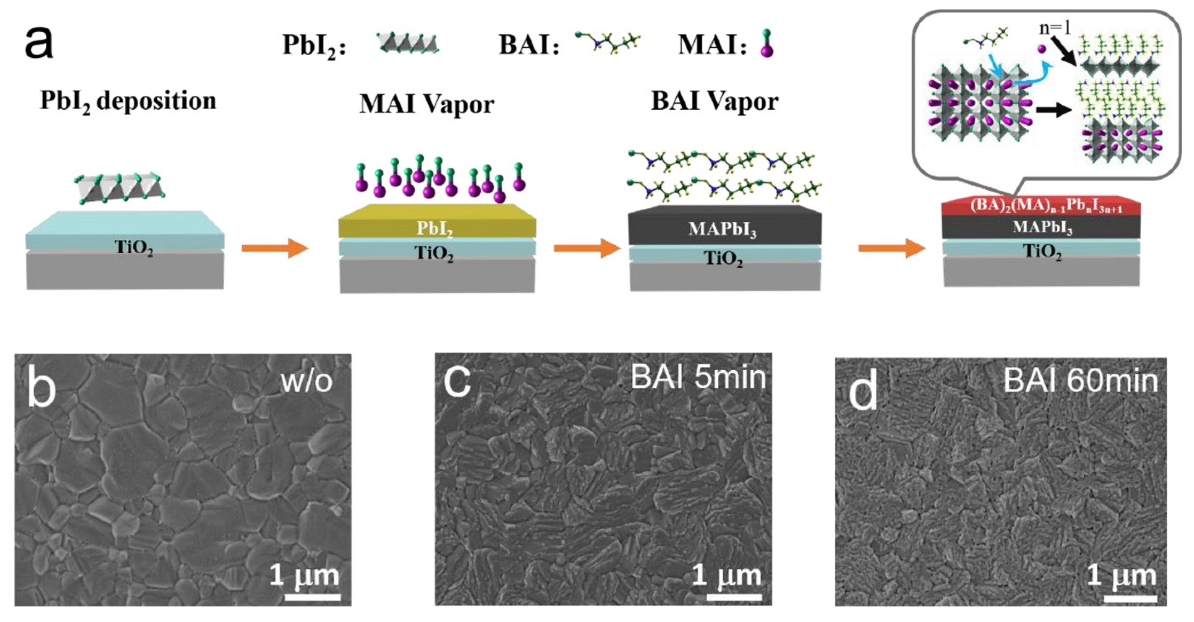
- In most studies, isopropyl alcohol (IPA) is used as a solvent to make an organic ammonium halide solution, although it is not ideal for the 3D perovskite film. Instead of using IPA, the solvent-free method is developed, where the organic salts are deposited in the vapor phase to form a thin 2D capping layer on the surface of the 3D perovskite film. Through this process, Lin et al. [31] found better PSC stability against a relative humidity of 55% (see Figure 12a) and temperature of 80 °C (see Figure 12b).
- 2.
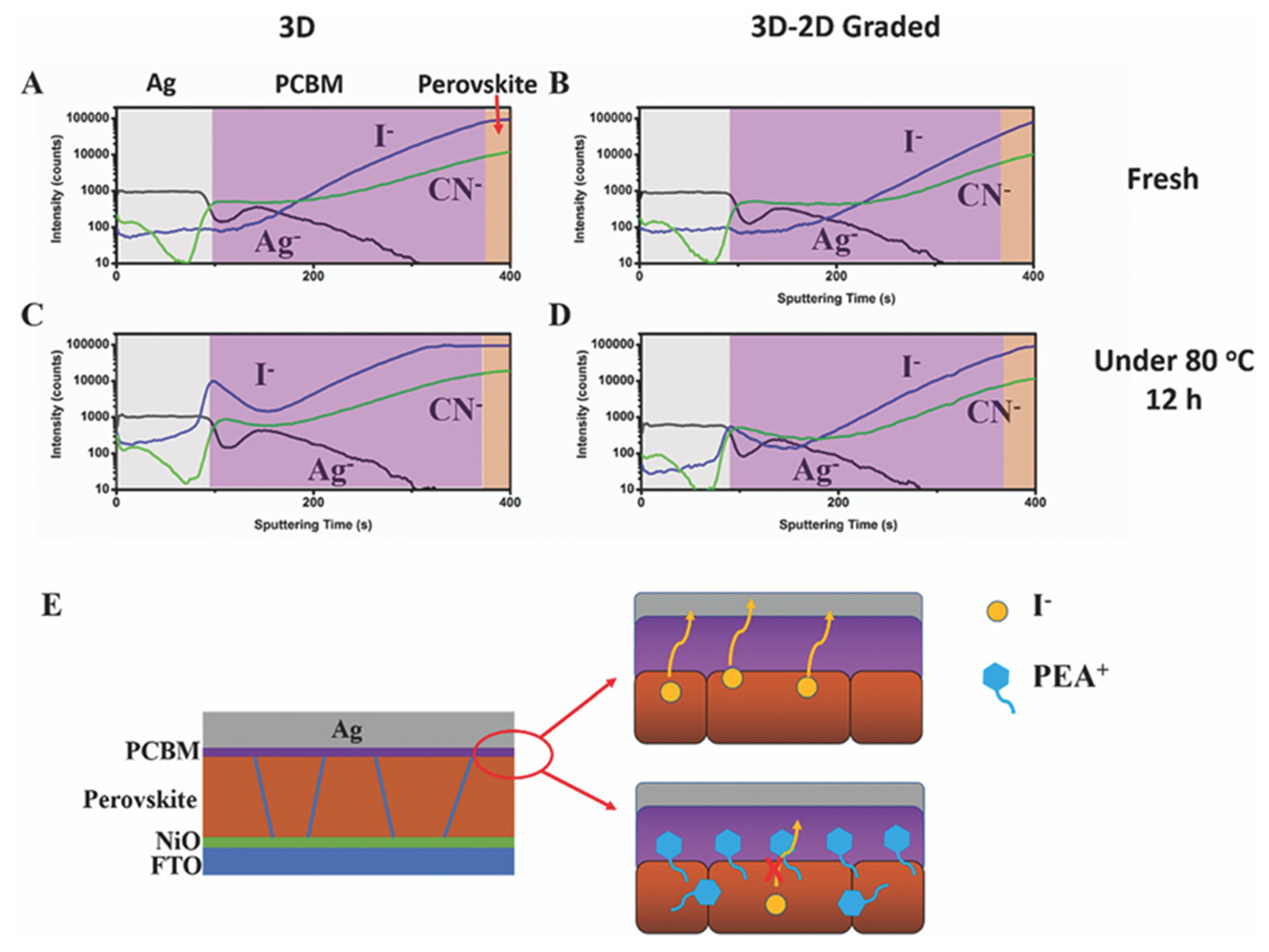
- Most studies find that halide ions diffuse immediately into the bulk because they are smaller and loosely bonded to the alkyl/arylammonium. Long or bulky organic cations also diffuse into the bulk under long-term thermal stress [75]. In long alkylammonium cations, the diffusion depends on the hydrocarbon chain length. Alan et al. [76] found that the 2D perovskite on top of the 3D perovskite thin film eventually transformed into a 3D perovskite under long-term thermal stress or illumination. They found that this transformation is slower for dodecylammonium compared to butylammonium. This indicates that the stability of the 3D/2D structure increases with the hydrocarbon chain length. Additionally, they found that the transformation process is even slower for 1,12-dodecanediammonium, suggesting that using diammonium alkaline ligands may be a possible pathway for forming a stable 3D/2D perovskite structure. In the case of arylammonium cations, it is challenging to prevent their diffusion into the bulk because they are smaller in size compared to alkylammonium cations. Park et al. [77] observed that fluorinated arylammonium offers better interfacial passivation and minimizes ligand intercalation reactivity with perovskites.
9. Conclusions
Funding
Conflicts of Interest
References
- Afroz, M.; Ratnesh, R.K.; Srivastava, S.; Singh, J. Perovskite Solar Cells: Progress, Challenges, and Future Avenues to Clean Energy. Sol. Energy 2025, 287, 113205. [Google Scholar] [CrossRef]
- Miglani, A.; Ogale, S.B.; Game, O.S. Architectural Innovations in Perovskite Solar Cells. Small 2025, 21, 2411355. [Google Scholar] [CrossRef] [PubMed]
- Gao, S.; Bae, J.-J.; Lee, D.S.; Yang, T.-Y.; Shin, S.S. Toward Sustainable Perovskite Solar Cells: From Lead-Free Materials to Environmental Concerns and Mitigation Strategies. EcoMat 2025, 7, e70001. [Google Scholar] [CrossRef]
- Seyisi, T.; Fouda-Mbanga, B.G.; Mnyango, J.I.; Nthwane, Y.B.; Nyoni, B.; Mhlanga, S.; Hlangothi, S.P.; Tywabi-Ngeva, Z. Major Challenges for Commercialization of Perovskite Solar Cells: A Critical Review. Energy Rep. 2025, 13, 1400–1415. [Google Scholar] [CrossRef]
- Kutsarov, D.I.; Rezaee, E.; Lambert, J.; Stroud, W.T.; Panagiotopoulos, A.; Silva, S.R.P. Progress in Flexible Perovskite Solar Cells: Paving the Way for Scalable Manufacturing. Adv. Mater. Technol. 2025, 2401834. [Google Scholar] [CrossRef]
- Biewald, A.; Giesbrecht, N.; Bein, T.; Docampo, P.; Hartschuh, A.; Ciesielski, R. Temperature-Dependent Ambipolar Charge Carrier Mobility in Large-Crystal Hybrid Halide Perovskite Thin Films. ACS Appl. Mater. Interfaces 2019, 11, 20838–20844. [Google Scholar] [CrossRef]
- Akel, S.; Kulkarni, A.; Rau, U.; Kirchartz, T. Relevance of Long Diffusion Lengths for Efficient Halide Perovskite Solar Cells. PRX Energy 2023, 2, 013004. [Google Scholar] [CrossRef]
- Chauhan, K.K.; Prodhan, S.; Ghosh, D.; Waghale, P.; Bhattacharyya, S.; Dutta, P.K.; Datta, P.K. Long Carrier Diffusion Length and Slow Hot Carrier Cooling in Thin Film Mixed Halide Perovskite. IEEE J. Photovolt. 2020, 10, 803–810. [Google Scholar] [CrossRef]
- Tan, S.; Yavuz, I.; Weber, M.H.; Huang, T.; Chen, C.-H.; Wang, R.; Wang, H.-C.; Ko, J.H.; Nuryyeva, S.; Xue, J.; et al. Shallow Iodine Defects Accelerate the Degradation of α-Phase Formamidinium Perovskite. Joule 2020, 4, 2426–2442. [Google Scholar] [CrossRef]
- Zhu, X.; Xiong, W.; Hu, C.; Mo, K.; Yang, M.; Li, Y.; Li, R.; Shen, C.; Liu, Y.; Liu, X.; et al. Constructing Ultra-Shallow Near-Edge States for Efficient and Stable Perovskite Solar Cells. Adv. Mater. 2024, 36, 2309487. [Google Scholar] [CrossRef]
- Kim, G.-W.; Petrozza, A. Defect Tolerance and Intolerance in Metal-Halide Perovskites. Adv. Energy Mater. 2020, 10, 2001959. [Google Scholar] [CrossRef]
- Cho, S.H.; Byeon, J.; Jeong, K.; Hwang, J.; Lee, H.; Jang, J.; Lee, J.; Kim, T.; Kim, K.; Choi, M.; et al. Investigation of Defect-Tolerant Perovskite Solar Cells with Long-Term Stability via Controlling the Self-Doping Effect. Adv. Energy Mater. 2021, 11, 2100555. [Google Scholar] [CrossRef]
- Zhang, X.; Turiansky, M.E.; Van de Walle, C.G. Correctly Assessing Defect Tolerance in Halide Perovskites. J. Phys. Chem. C 2020, 124, 6022–6027. [Google Scholar] [CrossRef]
- Frost, J.M.; Walsh, A. What Is Moving in Hybrid Halide Perovskite Solar Cells? Acc. Chem. Res. 2016, 49, 528–535. [Google Scholar] [CrossRef]
- Bag, M.; Renna, L.A.; Adhikari, R.Y.; Karak, S.; Liu, F.; Lahti, P.M.; Russell, T.P.; Tuominen, M.T.; Venkataraman, D. Kinetics of Ion Transport in Perovskite Active Layers and Its Implications for Active Layer Stability. J. Am. Chem. Soc. 2015, 137, 13130–13137. [Google Scholar] [CrossRef]
- Liu, P.; Wang, W.; Liu, S.; Yang, H.; Shao, Z. Fundamental Understanding of Photocurrent Hysteresis in Perovskite Solar Cells. Adv. Energy Mater. 2019, 9, 1803017. [Google Scholar] [CrossRef]
- Elumalai, N.K.; Uddin, A. Hysteresis in Organic-Inorganic Hybrid Perovskite Solar Cells. Sol. Energy Mater. Sol. Cells 2016, 157, 476–509. [Google Scholar] [CrossRef]
- Habisreutinger, S.N.; Noel, N.K.; Snaith, H.J. Hysteresis Index: A Figure without Merit for Quantifying Hysteresis in Perovskite Solar Cells. ACS Energy Lett. 2018, 3, 2472–2476. [Google Scholar] [CrossRef]
- Liu, X.; Luo, D.; Lu, Z.-H.; Yun, J.S.; Saliba, M.; Seok, S.I.; Zhang, W. Stabilization of Photoactive Phases for Perovskite Photovoltaics. Nat. Rev. Chem. 2023, 7, 462–479. [Google Scholar] [CrossRef]
- Qiu, Z.; Li, N.; Huang, Z.; Chen, Q.; Zhou, H. Recent Advances in Improving Phase Stability of Perovskite Solar Cells. Small Methods 2020, 4, 1900877. [Google Scholar] [CrossRef]
- Gong, J.B.; Darling, S.; You, F. Perovskite Photovoltaics: Life-Cycle Assessment of Energy and Environmental Impacts. Energy Environ. Sci. 2015, 8, 1953–1968. [Google Scholar] [CrossRef]
- Ahn, N.; Choi, M. Towards Long-Term Stable Perovskite Solar Cells: Degradation Mechanisms and Stabilization Techniques. Adv. Sci. 2024, 11, 2306110. [Google Scholar] [CrossRef] [PubMed]
- Bagade, S.S.; Patel, P.K. A Comprehensive Review on Potential of Diffusion Length Enhancement to Upraise Perovskite Solar Cell Performance. Phys. Scr. 2024, 99, 052003. [Google Scholar] [CrossRef]
- Howlader, A.H.; Uddin, A. Progress and Challenges of Chloride–Iodide Perovskite Solar Cells: A Critical Review. Nanomanufacturing 2023, 3, 177–216. [Google Scholar] [CrossRef]
- Howlader, A.H.; Dipta, S.S.; Tarique, W.B.; Qi, Y.; Pratik, A.; Yin, Y.; Hossain, M.A.; Uddin, A. Self-Formation of SnCl2 Passivation Layer on SnO2 Electron-Transport Layer in Chloride–Iodide-Based Perovskite Solar Cell. Adv. Energy Sustain. Res. 2024, 5, 2400030. [Google Scholar] [CrossRef]
- Chen, P.; Bai, Y.; Wang, S.; Lyu, M.; Yun, J.-H.; Wang, L. In Situ Growth of 2D Perovskite Capping Layer for Stable and Efficient Perovskite Solar Cells. Adv. Funct. Mater. 2018, 28, 1706923. [Google Scholar] [CrossRef]
- Huang, X.; Bi, W.; Jia, P.; Tang, Y.; Lou, Z.; Hu, Y.; Cui, Q.; Hou, Y.; Teng, F. Enhanced Efficiency and Light Stability of Planar Perovskite Solar Cells by Diethylammonium Bromide Induced Large-Grain 2D/3D Hybrid Film. Org. Electron. 2019, 67, 101–108. [Google Scholar] [CrossRef]
- Alharbi, E.A.; Alyamani, A.Y.; Kubicki, D.J.; Uhl, A.R.; Walder, B.J.; Alanazi, A.Q.; Luo, J.; Burgos-Caminal, A.; Albadri, A.; Albrithen, H.; et al. Atomic-Level Passivation Mechanism of Ammonium Salts Enabling Highly Efficient Perovskite Solar Cells. Nat. Commun. 2019, 10, 3008. [Google Scholar] [CrossRef]
- Fei, C.; Zhou, M.; Ogle, J.; Smilgies, D.-M.; Whittaker-Brooks, L.; Wang, H. Self-Assembled Propylammonium Cations at Grain Boundaries and the Film Surface to Improve the Efficiency and Stability of Perovskite Solar Cells. J. Mater. Chem. A 2019, 7, 23739–23746. [Google Scholar] [CrossRef]
- Yoo, J.J.; Wieghold, S.; Sponseller, M.C.; Chua, M.R.; Bertram, S.N.; Hartono, N.T.P.; Tresback, J.S.; Hansen, E.C.; Correa-Baena, J.-P.; Bulović, V.; et al. An Interface Stabilized Perovskite Solar Cell with High Stabilized Efficiency and Low Voltage Loss. Energy Environ. Sci. 2019, 12, 2192–2199. [Google Scholar] [CrossRef]
- Lin, D.; Zhang, T.; Wang, J.; Long, M.; Xie, F.; Chen, J.; Wu, B.; Shi, T.; Yan, K.; Xie, W.; et al. Stable and Scalable 3D-2D Planar Heterojunction Perovskite Solar Cells via Vapor Deposition. Nano Energy 2019, 59, 619–625. [Google Scholar] [CrossRef]
- Liu, Z.; Meng, K.; Wang, X.; Qiao, Z.; Xu, Q.; Li, S.; Cheng, L.; Li, Z.; Chen, G. In Situ Observation of Vapor-Assisted 2D–3D Heterostructure Formation for Stable and Efficient Perovskite Solar Cells. Nano Lett. 2020, 20, 1296–1304. [Google Scholar] [CrossRef] [PubMed]
- Mahmud, M.A.; Duong, T.; Yin, Y.; Pham, H.T.; Walter, D.; Peng, J.; Wu, Y.; Li, L.; Shen, H.; Wu, N.; et al. Double-Sided Surface Passivation of 3D Perovskite Film for High-Efficiency Mixed-Dimensional Perovskite Solar Cells. Adv. Funct. Mater. 2020, 30, 1907962. [Google Scholar] [CrossRef]
- Koh, T.M.; Shanmugam, V.; Guo, X.; Lim, S.S.; Filonik, O.; Herzig, E.M.; Müller-Buschbaum, P.; Swamy, V.; Chien, S.T.; Mhaisalkar, S.G.; et al. Enhancing Moisture Tolerance in Efficient Hybrid 3D/2D Perovskite Photovoltaics. J. Mater. Chem. A 2018, 6, 2122–2128. [Google Scholar] [CrossRef]
- Lv, Y.; Song, X.; Yin, Y.; Feng, Y.; Ma, H.; Hao, C.; Jin, S.; Shi, Y. Hexylammonium Iodide Derived Two-Dimensional Perovskite as Interfacial Passivation Layer in Efficient Two-Dimensional/Three-Dimensional Perovskite Solar Cells. ACS Appl. Mater. Interfaces 2020, 12, 698–705. [Google Scholar] [CrossRef]
- Cho, Y.; Soufiani, A.M.; Yun, J.S.; Kim, J.; Lee, D.S.; Seidel, J.; Deng, X.; Green, M.A.; Huang, S.; Ho-Baillie, A.W.Y. Mixed 3D–2D Passivation Treatment for Mixed-Cation Lead Mixed-Halide Perovskite Solar Cells for Higher Efficiency and Better Stability. Adv. Energy Mater. 2018, 8, 1703392. [Google Scholar] [CrossRef]
- Liu, X.; Webb, T.; Dai, L.; Ji, K.; Smith, J.A.; Kilbride, R.C.; Yavari, M.; Bi, J.; Ren, A.; Huang, Y.; et al. Influence of Halide Choice on Formation of Low-Dimensional Perovskite Interlayer in Efficient Perovskite Solar Cells. Energy Environ. Mater. 2022, 5, 670–682. [Google Scholar] [CrossRef]
- Zhuang, J.; Mao, P.; Luan, Y.; Yi, X.; Tu, Z.; Zhang, Y.; Yi, Y.; Wei, Y.; Chen, N.; Lin, T.; et al. Interfacial Passivation for Perovskite Solar Cells: The Effects of the Functional Group in Phenethylammonium Iodide. ACS Energy Lett. 2019, 4, 2913–2921. [Google Scholar] [CrossRef]
- Othman, M.; Zhang, T.; McMeekin, D.P.; Fürer, S.O.; Mao, W.; Li, W.; Scully, A.D.; Chesman, A.S.R.; Nakashima, P.N.H.; Bach, U.; et al. Structural and Photophysical Properties of Guanidinium–Iodide-Treated Perovskite Solar Cells. Solar RRL 2023, 7, 2200852. [Google Scholar] [CrossRef]
- Jeong, S.; Seo, S.; Yang, H.; Park, H.; Shin, S.; Ahn, H.; Lee, D.; Park, J.H.; Park, N.-G.; Shin, H. Cyclohexylammonium-Based 2D/3D Perovskite Heterojunction with Funnel-Like Energy Band Alignment for Efficient Solar Cells (23.91%). Adv. Energy Mater. 2021, 11, 2102236. [Google Scholar] [CrossRef]
- Li, B.; Xiang, Y.; Jayawardena, K.D.G.I.; Luo, D.; Wang, Z.; Yang, X.; Watts, J.F.; Hinder, S.; Sajjad, M.T.; Webb, T.; et al. Reduced Bilateral Recombination by Functional Molecular Interface Engineering for Efficient Inverted Perovskite Solar Cells. Nano Energy 2020, 78, 105249. [Google Scholar] [CrossRef]
- Kim, H.; Pei, M.; Lee, Y.; Sutanto, A.A.; Paek, S.; Queloz, V.I.E.; Huckaba, A.J.; Cho, K.T.; Yun, H.J.; Yang, H.; et al. Self-Crystallized Multifunctional 2D Perovskite for Efficient and Stable Perovskite Solar Cells. Adv. Funct. Mater. 2020, 30, 1910620. [Google Scholar] [CrossRef]
- Zhou, Y.; Wang, F.; Cao, Y.; Wang, J.-P.; Fang, H.-H.; Loi, M.A.; Zhao, N.; Wong, C.-P. Benzylamine-Treated Wide-Bandgap Perovskite with High Thermal-Photostability and Photovoltaic Performance. Adv. Energy Mater. 2017, 7, 1701048. [Google Scholar] [CrossRef]
- Hossain Howlader, A.; Binte Tarique, W.; Safat Dipta, S.; Pratik, A.; Yin, Y.; Uddin, A. Defects Passivation in Chloride-Iodide Perovskite Solar Cell with Chlorobenzylammonium Halides. Solar Energy 2024, 282, 112968. [Google Scholar] [CrossRef]
- Lee, H.B.; Kumar, N.; Devaraj, V.; Tyagi, B.; He, S.; Sahani, R.; Ko, K.-J.; Oh, J.-W.; Kang, J.-W. Trifluoromethyl-Group Bearing, Hydrophobic Bulky Cations as Defect Passivators for Highly Efficient, Stable Perovskite Solar Cells. Solar RRL 2021, 5, 2100712. [Google Scholar] [CrossRef]
- Zhu, H.; Ren, Y.; Pan, L.; Ouellette, O.; Eickemeyer, F.T.; Wu, Y.; Li, X.; Wang, S.; Liu, H.; Dong, X.; et al. Synergistic Effect of Fluorinated Passivator and Hole Transport Dopant Enables Stable Perovskite Solar Cells with an Efficiency Near 24%. J. Am. Chem. Soc. 2021, 143, 3231–3237. [Google Scholar] [CrossRef]
- La-Placa, M.-G.; Gil-Escrig, L.; Guo, D.; Palazon, F.; Savenije, T.J.; Sessolo, M.; Bolink, H.J. Vacuum-Deposited 2D/3D Perovskite Heterojunctions. ACS Energy Lett. 2019, 4, 2893–2901. [Google Scholar] [CrossRef]
- Niu, T.; Lu, J.; Jia, X.; Xu, Z.; Tang, M.-C.; Barrit, D.; Yuan, N.; Ding, J.; Zhang, X.; Fan, Y.; et al. Interfacial Engineering at the 2D/3D Heterojunction for High-Performance Perovskite Solar Cells. Nano Lett. 2019, 19, 7181–7190. [Google Scholar] [CrossRef]
- Bai, Y.; Xiao, S.; Hu, C.; Zhang, T.; Meng, X.; Lin, H.; Yang, Y.; Yang, S. Dimensional Engineering of a Graded 3D–2D Halide Perovskite Interface Enables Ultrahigh Voc Enhanced Stability in the p-i-n Photovoltaics. Adv. Energy Mater. 2017, 7, 1701038. [Google Scholar] [CrossRef]
- Degani, M.; An, Q.; Albaladejo-Siguan, M.; Hofstetter, Y.J.; Cho, C.; Paulus, F.; Grancini, G.; Vaynzof, Y. 23.7% Efficient Inverted Perovskite Solar Cells by Dual Interfacial Modification. Sci. Adv. 2021, 7, eabj7930. [Google Scholar] [CrossRef]
- Larini, V.; Degani, M.; Pica, G.; Ding, C.; Andaji-Garmaroudi, Z.; Faini, F.; Stranks, S.D.; Ma, C.-Q.; Grancini, G. From Bulk to Surface Passivation: Double Role of Chlorine-Doping for Boosting Efficiency of FAPbI3-Rich Perovskite Solar Cells. Solar RRL 2022, 6, 2200038. [Google Scholar] [CrossRef]
- Yang, Z.; Chen, J.; Li, M.; Qi, M.; Zhang, G.; Chen, R.; Hu, J.; Liu, X.; Qin, C.; Xiao, L.; et al. 4-Methoxy Phenethylammonium Halide Salts for Surface Passivation of Perovskite Films towards Efficient and Stable Solar Cells. Chem. Eng. J. 2024, 494, 152955. [Google Scholar] [CrossRef]
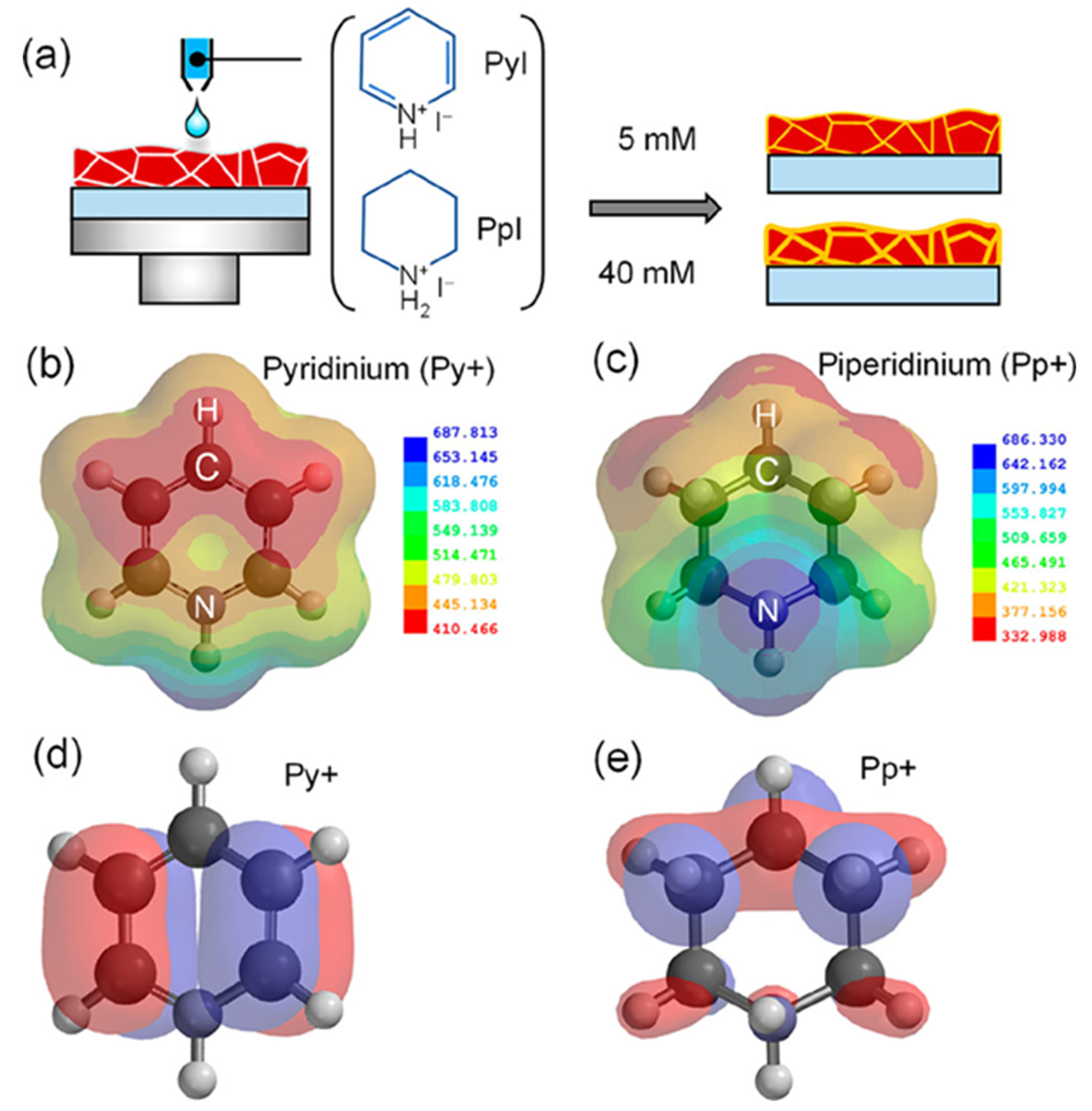
- Du, Y.; Wu, J.; Zhang, X.; Zhu, Q.; Zhang, M.; Liu, X.; Zou, Y.; Wang, S.; Sun, W. Surface Passivation Using Pyridinium Iodide for Highly Efficient Planar Perovskite Solar Cells. J. Energy Chem. 2021, 52, 84–91. [Google Scholar] [CrossRef]
- Kim, J.-H.; Kim, S.-G.; Park, N.-G. Effect of Chemical Bonding Nature of Post-Treatment Materials on Photovoltaic Performance of Perovskite Solar Cells. ACS Energy Lett. 2021, 6, 3435–3442. [Google Scholar] [CrossRef]
- Zhou, T.; Lai, H.; Liu, T.; Lu, D.; Wan, X.; Zhang, X.; Liu, Y.; Chen, Y. Highly Efficient and Stable Solar Cells Based on Crystalline Oriented 2D/3D Hybrid Perovskite. Adv. Mater. 2019, 31, 1901242. [Google Scholar] [CrossRef]
- Wen, L.; Deng, Y.; Zeng, G.; Liu, G.; Li, X. Surface-Bulk-Passivated Perovskite Films via 2-Thiophenemethylammonium Bromide and PbBr2 for Air-Processed Perovskite Solar Cells with High-Stability. Chem. Eng. J. 2023, 468, 143446. [Google Scholar] [CrossRef]
- Sutanto, A.A.; Drigo, N.; Queloz, V.I.E.; Garcia-Benito, I.; Kirmani, A.R.; Richter, L.J.; Schouwink, P.A.; Cho, K.T.; Paek, S.; Nazeeruddin, M.K.; et al. Dynamical Evolution of the 2D/3D Interface: A Hidden Driver Behind Perovskite Solar Cell Instability. J. Mater. Chem. A 2020, 8, 2343–2348. [Google Scholar] [CrossRef]
- Mahmud, M.A.; Pham, H.T.; Duong, T.; Yin, Y.; Peng, J.; Wu, Y.; Liang, W.; Li, L.; Kumar, A.; Shen, H.; et al. Combined Bulk and Surface Passivation in Dimensionally Engineered 2D-3D Perovskite Films via Chlorine Diffusion. Adv. Funct. Mater. 2021, 31, 2104251. [Google Scholar] [CrossRef]
- Fu, D.-W.; Zhang, W.; Cai, H.-L.; Ge, J.-Z.; Zhang, Y.; Xiong, R.-G. Diisopropylammonium Chloride: A Ferroelectric Organic Salt with a High Phase Transition Temperature and Practical Utilization Level of Spontaneous Polarization. Adv. Mater. 2011, 23, 5658–5662. [Google Scholar] [CrossRef]
- Wang, F.; Duan, D.; Singh, M.; Sutter-Fella, C.M.; Lin, H.; Li, L.; Naumov, P.; Hu, H. Ionic Liquid Engineering in Perovskite Photovoltaics. Energy Environ. Mater. 2023, 6, e12435. [Google Scholar] [CrossRef]
- Zhang, K.; Zhang, X.; Brooks, K.G.; Ding, B.; Kinge, S.; Ding, Y.; Dai, S.; Nazeeruddin, M.K. Role of Ionic Liquids in Perovskite Solar Cells. Solar RRL 2023, 7, 2300115. [Google Scholar] [CrossRef]
- Ma, J.; Wang, L.; He, K.; Sun, Y.; Li, B.; Zhao, Q.; Du, B. Progress and Challenges: A Review of Ionic Liquid Treatment for Efficient and Stable Perovskite Solar Cells. J. Mater. Chem. C 2024, 12, 10837–10856. [Google Scholar] [CrossRef]
- Chao, L.; Niu, T.; Xia, Y.; Chen, Y.; Huang, W. Ionic Liquid for Perovskite Solar Cells: An Emerging Solvent Engineering Technology. Acc. Mater. Res. 2021, 2, 1059–1070. [Google Scholar] [CrossRef]
- He, L.; Wu, H.; Lian, X.; Zuo, L.; Wu, G.; Chen, H. Efficient and Stable Inverted Perovskite Solar Cells Incorporating 4-Fluorobenzylammonium Iodide. Org. Electron. 2021, 92, 106124. [Google Scholar] [CrossRef]
- Ma, C.; Shen, D.; Huang, B.; Li, X.; Chen, W.-C.; Lo, M.-F.; Wang, P.; Lam, M.H.-W.; Lu, Y.; Ma, B.; et al. High Performance Low-Dimensional Perovskite Solar Cells Based on a One Dimensional Lead Iodide Perovskite. J. Mater. Chem. A 2019, 7, 8811–8817. [Google Scholar] [CrossRef]
- Nega, P.W.; Li, Z.; Ghosh, V.; Thapa, J.; Sun, S.; Hartono, N.T.P.; Nellikkal, M.A.N.; Norquist, A.J.; Buonassisi, T.; Chan, E.M.; et al. Using Automated Serendipity to Discover How Trace Water Promotes and Inhibits Lead Halide Perovskite Crystal Formation. Appl. Phys. Lett. 2021, 119, 041903. [Google Scholar] [CrossRef]
- Lin, R.; Xu, J.; Wei, M.; Wang, Y.; Qin, Z.; Liu, Z.; Wu, J.; Xiao, K.; Chen, B.; Park, S.M.; et al. All-Perovskite Tandem Solar Cells with Improved Grain Surface Passivation. Nature 2022, 603, 73–78. [Google Scholar] [CrossRef]
- Zou, S.; Ren, S.; Jiang, Y.; Huang, Y.; Wang, W.; Wang, C.; Chen, C.; Hao, X.; Wu, L.; Zhang, J.; et al. Efficient Environment-Friendly Lead-Free Tin Perovskite Solar Cells Enabled by Incorporating 4-Fluorobenzylammonium Iodide Additives. Energy Environ. Mater. 2023, 6, e12465. [Google Scholar] [CrossRef]
- Li, B.; Deng, J.; Smith, J.A.; Caprioglio, P.; Ji, K.; Luo, D.; McGettrick, J.D.; Jayawardena, K.D.G.I.; Kilbride, R.C.; Ren, A.; et al. Suppressing Interfacial Recombination with a Strong-Interaction Surface Modulator for Efficient Inverted Perovskite Solar Cells. Adv. Energy Mater. 2022, 12, 2202868. [Google Scholar] [CrossRef]
- Sutanto, A.A.; Caprioglio, P.; Drigo, N.; Hofstetter, Y.J.; Garcia-Benito, I.; Queloz, V.I.E.; Neher, D.; Nazeeruddin, M.K.; Stolterfoht, M.; Vaynzof, Y.; et al. 2D/3D Perovskite Engineering Eliminates Interfacial Recombination Losses in Hybrid Perovskite Solar Cells. Chem 2021, 7, 1903–1916. [Google Scholar] [CrossRef]
- Jang, Y.-W.; Lee, S.; Yeom, K.M.; Jeong, K.; Choi, K.; Choi, M.; Noh, J.H. Intact 2D/3D Halide Junction Perovskite Solar Cells via Solid-Phase in-Plane Growth. Nat. Energy 2021, 6, 63–71. [Google Scholar] [CrossRef]
- Sherkar, T.S.; Momblona, C.; Gil-Escrig, L.; Ávila, J.; Sessolo, M.; Bolink, H.J.; Koster, L.J.A. Recombination in Perovskite Solar Cells: Significance of Grain Boundaries, Interface Traps, and Defect Ions. ACS Energy Lett. 2017, 2, 1214–1222. [Google Scholar] [CrossRef] [PubMed]
- Yuan, Y.; Huang, J. Ion Migration in Organometal Trihalide Perovskite and Its Impact on Photovoltaic Efficiency and Stability. Acc. Chem. Res. 2016, 49, 286–293. [Google Scholar] [CrossRef] [PubMed]
- Yin, W.-J.; Shi, T.; Yan, Y. Unusual Defect Physics in CH3NH3PbI3 Perovskite Solar Cell Absorber. Appl. Phys. Lett. 2014, 104, 063903. [Google Scholar] [CrossRef]
- Perini, C.A.R.; Rojas-Gatjens, E.; Ravello, M.; Castro-Mendez, A.-F.; Hidalgo, J.; An, Y.; Kim, S.; Lai, B.; Li, R.; Silva-Acuña, C.; et al. Interface Reconstruction from Ruddlesden–Popper Structures Impacts Stability in Lead Halide Perovskite Solar Cells. Adv. Mater. 2022, 34, 2204726. [Google Scholar] [CrossRef]
- Kaplan, A.B.; Burlingame, Q.C.; Ivancevic, M.R.; Loo, Y.-L. Understanding the Structural Dynamics of 2D/3D Perovskite Interfaces. ACS Appl. Mater. Interfaces 2025, 17, 16963–16969. [Google Scholar] [CrossRef]
- Park, S.M.; Wei, M.; Xu, J.; Atapattu, H.R.; Eickemeyer, F.T.; Darabi, K.; Grater, L.; Yang, Y.; Liu, C.; Teale, S.; et al. Engineering Ligand Reactivity Enables High-Temperature Operation of Stable Perovskite Solar Cells. Science 2023, 381, 209–215. [Google Scholar] [CrossRef]


| Chemical Name (2D Layer) | Structural Formula (2D Layer) | Chemical Formula (3D Layer) | Voc (V) | Jsc (mA/cm2) | FF (%) | PCE (%) | Stability (Hours) | Ref. |
|---|---|---|---|---|---|---|---|---|
| Ethylammonium |  | FA0.9Cs0.07MA0.03Pb(I0.92Br0.08)3 | 1.12 | 24.36 | 80.4 | 22.30 | 550 (90%) | [28] |
| Cs0.05FA0.80MA0.15Pb(I0.85Br0.15)3 | 1.12 | 21.81 | 75 | 18.92 | - | [29] | ||
| Propylammonium | 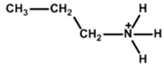 | Cs0.05FA0.80MA0.15Pb(I0.85Br0.15)3 | 1.13 | 22.26 | 78 | 20.25 | - | [29] |
| Butylammonium | 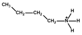 | Cs0.05FA0.80MA0.15Pb(I0.85Br0.15)3 | 1.11 | 22.01 | 76 | 19.43 | - | [29] |
| (FAPbI3)0.92(MAPbBr3)0.08 | 1.14 | 24 | 79.90 | 22 | 2400 (90%) | [30] | ||
| MAPbI3 | 1.02 | 23.37 | 68.70 | 16.50 | 7200 (74%) | [31] | ||
| MAPbI3 | 1.16 | 20.89 | 80.40 | 19.48 | 600 (92%) | [32] | ||
| Cs0.07Rb0.03FA0.765MA0.135PbI2.55Br0.45 | 1.20 | 23.94 | 79.31 | 22.77 | 20 (90%) | [33] | ||
| Cs0.05(MA0.17FA0.83)Pb(I0.83Br0.17)3 | 1.06 | 19.40 | 76.69 | 15.74 | 100 (86%) | [34] | ||
| Cs0.07FA0.79MA0.14Pb(I0.88Br0.12)3 | 1.12 | 22.95 | 75 | 19.43 | 1200 (99%) | [35] | ||
| Hexylammonium | 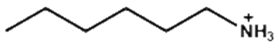 | (FAPbI3)0.92(MAPbBr3)0.08 | 1.15 | 24.20 | 80.30 | 22.40 | 2400 (95%) | [30] |
| Cs0.07FA0.79MA0.14Pb(I0.88Br0.12)3 | 1.14 | 23.76 | 76 | 20.62 | 1200 (99%) | [35] | ||
| Octylammonium | 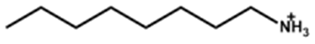 | (FAPbI3)0.92(MAPbBr3)0.08 | 1.15 | 24.20 | 79.80 | 22.10 | 2400 (99%) | [30] |
| Cs0.05(MA0.17FA0.83)Pb(I0.83Br0.17)3 | 1.02 | 19.37 | 76.70 | 15.19 | - | [34] | ||
| Iso-Butlammonium | 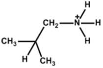 | (FAPbI3)0.85(MAPbBr3)0.15 | 1 | - | - | 21.7 | 912 (87%) | [36] |
| Tert-Pentylammonium | 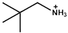 | FA(MA)PbI3 | 1.16 | 24.71 | 81.62 | 23.35 | 1500 (95%) | [37] |
| Diethylammonium | 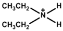 | MAPbI3 | 1.06 | 21.93 | 78.70 | 18.30 | 60 (90%) | [27] |
| 2-Methoxyethylammonium | 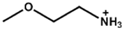 | (FAPbI3)1–x(MAPbBr3–yCly)x | 1.08 | 23.79 | 69.07 | 17.74 | - | [38] |
| Guanidinium |  | FA0.9Cs0.07MA0.03Pb(I0.92Br0.08)3 | 1.106 | 24.45 | 75.3 | 20.90 | 550 h (90%) | [28] |
| Cs0.07MA0.14FA0.79Pb(I0.83Br0.17)3 | 1.2 | 22.8 | 75.1 | 18.2 | - | [39] | ||
| Cyclohexylammonium | 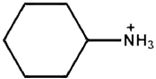 | FAPbI3 | 1.13 | 24.72 | 83.06 | 23.10 | 200 s (93%) | [40] |
| Cyclohexyl-methylammonium |  | FAPbI3 | 1.14 | 24.83 | 84.25 | 23.91 | 200 s (97%) | [40] |
| Chemical Name (2D Layer) | Structural Formula (2D Layer) | Chemical Formula (3D Layer) | Voc (V) | Jsc (mA/cm2) | FF (%) | PCE (%) | Stability (Hours) | Ref. |
|---|---|---|---|---|---|---|---|---|
| Phenylammonium |  | Cs0.05FA0.79MA0.16PbI2.4Br0.6 | 1.18 | 21.19 | 83 | 21.33 | 550 h (70%) | [41] |
| Benzylammonium | 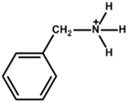 | Cs0.08FA0.77MA0.12PbI2.62Br0.35 | 1.08 | 24.48 | 78.80 | 20.79 | 600 h (80%) | [42] |
| FA0.15Cs0.85Pb(I0.73Br0.27)3 | 1.24 | 19.83 | 73.70 | 18.13 | 960 h (80%) | [43] | ||
| 4-Chloro-Benzylammonium | 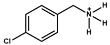 | FA0.6MA0.4PbI2.7Cl0.3 | 1.12 | 25.69 | 72.78 | 21 | 672 h (88%) | [44] |
| 4-Trifluoromethyl-Benzylammonium | 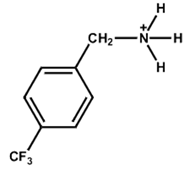 | FA0.85MA0.15PbBr0.45I2.55 | 1.16 | 22.21 | 81.25 | 20.75 | 300 h (86%) | [45] |
| Cs0.05FA0.85MA0.10Pb(I0.97Br0.03)3 | 1.16 | 24.98 | 82.40 | 23.94 | 500 h (96.5%) | [46] | ||
| Phenethylammonium | 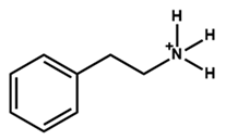 | MAPbI3 | 1.06 | 21.80 | 76.60 | 17.70 | - | [47] |
| Cs0.05(FA0.83MA0.17)0.95Pb(I0.83Br0.17)3 | 1.11 | 73 | 22.89 | 18.91 | 1000 h (90%) | [26] | ||
| Cs0.1FA0.74MA0.13PbI2.48Br0.39 | 1.14 | 24.20 | 76.60 | 21.15 | 1440 h (84%) | [48] | ||
| MAPbI3 | 1.17 | 21.80 | 78 | 19.89 | 720 h (96%) | [49] | ||
| Cs0.1FA0.77MA0.13PbI2.59Br0.41 | 1.14 | 23.43 | 77.4 | 20.62 | - | |||
| 4-Chloro-Phenethylammonium |  | Cs0.05(FA5/6MA1/6)0.95Pb(I0.85Br0.15)3 | 1.15 | 23.68 | 85 | 23.07 | 33 h (90%) | [50] |
| 4-Fluoro-Phenethylammonium | 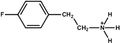 | Cs0.05(FA5/6MA1/6)0.95Pb(I0.85Br0.15)3 | 1.16 | 24.13 | 84.60 | 23.72 | 33 h (90%) | [50] |
| Cs0.1FA0.77MA0.13PbI2.59Br0.41 | 1.13 | 23.21 | 78.40 | 20.53 | - | |||
| 4-Methyl-Phenethylammonium |  | FAPbI3 | 1.10 | 24.76 | 78.6 | 21.4 | - | [51] |
| (FAPbI3)1–x(MAPbBr3–yCly)x | 1.16 | 24.49 | 76.94 | 21.85 | - | [38] | ||
| 4-Methoxy-Phenethylammonium |  | Cs0.15FA0.85Pb(I0.95Br0.05)3 | 1.13 | 24.33 | 82.31 | 22.63 | 1000 h (84%) | [52] |
| (FAPbI3)1–x(MAPbBr3–yCly)x | 1.18 | 25.04 | 77.79 | 22.98 | 1000 h (89%) | [38] |
| Chemical Name (2D Layer) | Structural Formula (2D Layer) | Chemical Formula (3D Layer) | Voc (V) | Jsc (mA/cm2) | FF (%) | PCE (%) | Stability (Hours) | Ref. |
|---|---|---|---|---|---|---|---|---|
| Pyridinium |  | Cs0.05(MA0.17FA0.83)0.95Pb(I0.83Br0.17)3 | 1.19 | 23.12 | 78 | 21.42 | 720 h (81.40%) | [53] |
| FA0.9Cs0.1PbI2.8Br0.2 | 1.15 | 23.70 | 81.20 | 22.26 | 0.5 h (115.01%) | [54] | ||
| Piperidinium | 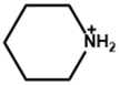 | FA0.9Cs0.1PbI2.8Br0.2 | 1.15 | 23.58 | 80.49 | 21.77 | 0.5 h (99.40%) | [54] |
| Imidazolium | 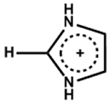 | FA0.9Cs0.07MA0.03Pb(I0.92Br0.08)3 | 1.10 | 24.14 | 79.40 | 21.60 | 550 h (90%) | [28] |
| 2-Thiophenemethylammonium | 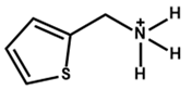 | CH3NH3PbI3 | 1.16 | 22.36 | 81 | 21.49% | 1680 h (99%) | [55] |
| - | 1.09 | 21.45 | 80.31 | 18.58 | 720 h (98) | [56] | ||
| [(FAPbI3)0.87(MAPbBr3)0.13]0.92(CsPbI3)0.08 | 1.13 | 23.50 | 75.10 | 19.97 | 1000 h (70%) | [57] | ||
| 2-Thiopheneethylammonium | 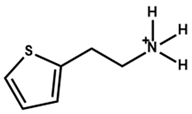 | Cs0.05FA0.79MA0.16PbBr0.6I2.4 | 1.2 | 21.93 | 83 | 21.09 | - | [55] |
| [(FAPbI3)0.87(MAPbBr3)0.13]0.92(CsPbI3)0.08 | 1.12 | 23.60 | 76.50 | 19.42 | 1000 h (90%) | [57] |
Disclaimer/Publisher’s Note: The statements, opinions and data contained in all publications are solely those of the individual author(s) and contributor(s) and not of MDPI and/or the editor(s). MDPI and/or the editor(s) disclaim responsibility for any injury to people or property resulting from any ideas, methods, instructions or products referred to in the content. |
© 2025 by the authors. Licensee MDPI, Basel, Switzerland. This article is an open access article distributed under the terms and conditions of the Creative Commons Attribution (CC BY) license (https://creativecommons.org/licenses/by/4.0/).
Share and Cite
Howlader, A.H.; Uddin, A. Progress and Challenges of Three-Dimensional/Two-Dimensional Bilayered Perovskite Solar Cells: A Critical Review. Nanomaterials 2025, 15, 876. https://doi.org/10.3390/nano15120876
Howlader AH, Uddin A. Progress and Challenges of Three-Dimensional/Two-Dimensional Bilayered Perovskite Solar Cells: A Critical Review. Nanomaterials. 2025; 15(12):876. https://doi.org/10.3390/nano15120876
Chicago/Turabian StyleHowlader, Ashraful Hossain, and Ashraf Uddin. 2025. "Progress and Challenges of Three-Dimensional/Two-Dimensional Bilayered Perovskite Solar Cells: A Critical Review" Nanomaterials 15, no. 12: 876. https://doi.org/10.3390/nano15120876
APA StyleHowlader, A. H., & Uddin, A. (2025). Progress and Challenges of Three-Dimensional/Two-Dimensional Bilayered Perovskite Solar Cells: A Critical Review. Nanomaterials, 15(12), 876. https://doi.org/10.3390/nano15120876