Article

Effects of Deposition Power and Annealing Temperature on Indium Zinc Oxide (IZO) Film’s Properties and Their Applications to the Source–Drain Electrodes of Amorphous Indium Gallium Zinc Oxide (a-IGZO) Thin-Film Transistors (TFTs)

1
Department of Semiconductor and Electro-Optical Technology, Minghsin University of Science and Technology, Hsinchu 30401, Taiwan
2
Department of Electronic Engineering, Minghsin University of Science and Technology, Hsinchu 30401, Taiwan
3
Department of Materials Science and Engineering, National Yang Ming Chiao Tung University, Hsinchu 30010, Taiwan
4
Institute of Electronics, National Yang Ming Chiao Tung University, 1001 Ta-Hsueh Road, Hsinchu 300, Taiwan
*
Author to whom correspondence should be addressed.
Nanomaterials 2025, 15(11), 780; https://doi.org/10.3390/nano15110780
Submission received: 6 April 2025 / Revised: 15 May 2025 / Accepted: 19 May 2025 / Published: 22 May 2025
(This article belongs to the Special Issue Wide Bandgap Semiconductor Material, Device and System Integration)

Abstract

:
The optical, electrical, and material properties of In–Zn–O (IZO) films were optimized by adjusting the deposition power and annealing temperature. Films deposited at 125 W and annealed at 300 °C exhibited the best performance, with the lowest resistivity (1.43 × 10⁻³ Ω·cm), highest mobility (11.12 cm2/V·s), and highest carrier concentration (4.61 × 1020 cm−3). The average transmittance and optical energy gap were 82.57% and 3.372 eV, respectively. The electrical characteristics of amorphous In-Ga-Zn-O (a-IGZO) thin-film transistors (TFTs) using IZO source-drain (S–D) electrodes with various sputtering powers and annealing temperatures were investigated. The optimal sputtering power of 125 W and annealing temperature of 300 °C for the IZO S–D electrodes resulted in the highest field-effect mobility (~12.31 cm2/V·s) and on current (~2.09 × 10⁻⁶ A). This improvement is attributed to enhanced carrier concentration and mobility, which result from the high In/Zn ratio, the larger grain size, and low RMS roughness in the IZO films. The parasitic contact resistance (RSD) and channel resistance (RCH) were analyzed using the total resistance method. RSD decreased with increasing IZO S–D sputtering power, while RCH reached a minimum at 125 W. Both resistances decreased significantly as the annealing temperature increased from 200 °C to 300 °C.

1. Introduction

Indium gallium zinc oxide (IGZO) thin-film transistors (TFTs) are highly attractive for display applications due to their high transparency and excellent electrical properties, including a high mobility and a high on/off current ratio. These characteristics make them particularly appealing for use in brain-like synaptic transistors, back planes in CMOS image sensors, integrated circuits (ICs), flexible and wearable electronics, power switching circuits, BEOL transistor elements in 3D logic, and cell transistors in DRAM [1,2,3,4,5]. In general, the electrical performance of oxide semiconductor TFTs is related to the contact resistance between the channel layer and the source-drain (S–D) electrode materials, as well as the channel resistance [6,7,8,9,10]. Shimura et al. [6] used various contact materials, including silver (Ag), indium (In), titanium (Ti), indium tin oxide (ITO), and amorphous indium zinc oxide (a-IZO), to fabricate the contact layers of the devices and study their impact on contact resistance (ρC) under different processing conditions. The TFTs with ITO and Ti as the source and drain contact layers showed better device performance than those with gold (Au) Schottky contacts. Barquinha et al. [7] explored the possibility of replacing ITO with different materials in inverted staggered TFTs, which use IGZO as the semiconductor material. The electrode materials analyzed include IZO, Ti, aluminum (Al), molybdenum (Mo), and titanium/gold (Ti/Au). Each material was applied in two different devices: one where annealing was performed after the IGZO channel deposition and before the S–D deposition, and the other where annealing was performed at the end of the device fabrication. The results showed that the electrical characteristics improved when annealing was performed at the end of the device fabrication. Due to the potential formation of energy barriers at the interface between the IGZO channel layer and ITO thin films, when ITO is used as the S–D electrode for IGZO TFTs, an interface resistance may form between the two layers, affecting the device performance. Choi et al. [10] proposed an innovative design by co-sputtering IGZO and ITO mixed films at room temperature (with a thickness of 125 nm), followed by the deposition of a 375 nm thick ITO layer as the S–D electrode to fabricate TFTs. The proposed TFT demonstrates enhanced electrical performance, attributed to its lower contact and channel resistance, as well as the formation of a surface reaction between the S–D and channel layers, which generated additional oxygen vacancies in the IGZO channel region.
IZO thin films with excellent optical and electrical properties have been widely utilized in oxide thin-film transistors, including as materials for the source and drain regions, channel layers, and top gate electrodes of the dual-gate devices, by adjusting the reactive oxygen content in the sputter chamber during deposition, as well as by varying the annealing temperatures and atmospheres [11,12,13,14,15,16,17,18]. Research on IZO thin films primarily utilizes radio-frequency (RF) and DC magnetron sputtering technology and covers various processing conditions, such as different power, process pressure, oxygen flow rates, and substrate temperatures, as well as various annealing temperatures and variations in the annealing atmosphere [19,20,21,22,23]. The effects of various processing parameters on the structural, optical, and electrical characteristics of the IZO thin films have been studied. However, there has been limited research on the effects of IZO S–D electrode processes with varying deposition powers and annealing temperatures on the electrical characteristics of a-IGZO TFTs.
This study investigates the optical, electrical, and material properties of IZO films deposited at different RF magnetron sputtering powers under Ar and O2 atmospheres at room temperature. Following deposition, the films were annealed at various temperatures in an N2 atmosphere. Moreover, an inverted–staggered transistor structure was used on silicon wafers to fabricate IGZO TFTs in this work. The effects of IZO S–D electrode processes with varying sputtering powers and annealing temperatures on the transfer characteristics of a-IGZO TFTs were studied. Output characteristics of devices with different channel lengths (L) were analyzed using the total resistance method [24,25]; the channel resistance (RCH) and S–D contact resistance (RSD) at different sputtering powers and annealing temperatures of IZO were extracted and analyzed. The IGZO TFT device with an IZO electrode deposited at 125 W and annealed at 300 °C exhibited the highest field-effect mobility (μFE) and on current (Ion). This enhancement is attributed to the IZO film having the highest In/Zn atomic ratio, the largest average grain size, and the smoothest surface, as measured by energy-dispersive spectroscopy (EDS), X-ray diffraction (XRD), and atomic force microscopy (AFM), respectively. These properties lead to increased carrier mobility and concentration in the IZO films, resulting in reductions in the total resistance (Rtotal), contact resistance (RSD), and channel resistance (RCH) in a-IGZO TFTs with IZO S–D electrodes. This study aims to establish a causal relationship between the properties of IZO films and the characteristics of the source–drain electrodes in a-IGZO TFTs.

2. Materials and Methods

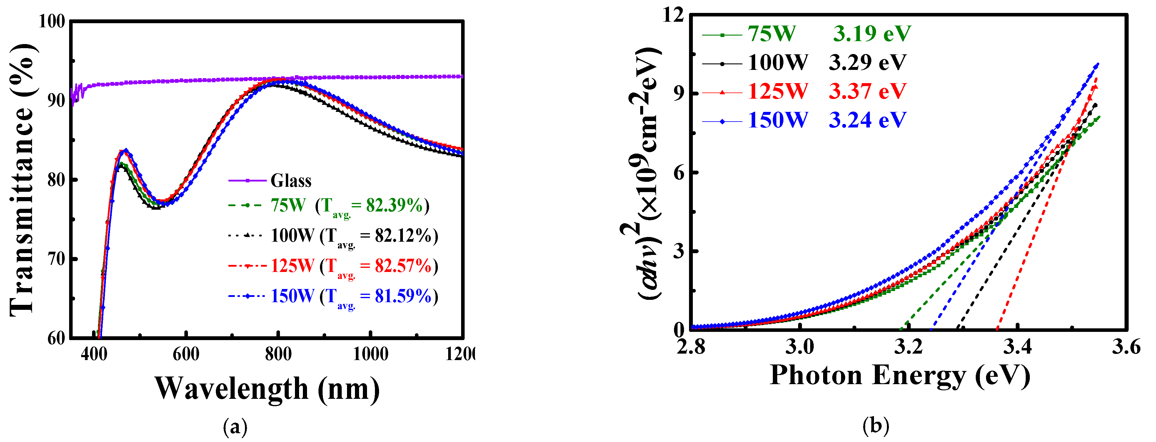
2.1. IZO Film Deposition and Characterization Measurements

IZO thin films were deposited at room temperature on B270 glass substrates and Si wafers using RF magnetron sputtering with a 7.62 cm (3-inch) diameter IZO target (In2O3: ZnO = 90 wt%: 10 wt%, 99.99% purity). The sputtering power was varied to 75 W, 100 W, 125 W, and 150 W. Prior to deposition, the chamber was evacuated to a base pressure of 5.3 × 10⁻⁴ Pa. Argon (50 sccm) and oxygen (1 sccm) gases were then introduced to maintain a working pressure of 0.67 Pa during the process. Following deposition, the films were annealed at 200 °C, 300 °C, and 350 °C for 1 h in a nitrogen (N2) ambient (40 sccm) condition at the same working pressure. Film resistivity, carrier mobility, and carrier concentration were determined using a Hall measurement system (HALL 8800, Swin, Hsinchu, Taiwan). The surface morphology and chemical composition of the IZO thin films were characterized using an ultra-high-resolution field-emission scanning electron microscope (FE-SEM, JEOL JSM-7800F Prime, Akishima, Tokyo, Japan) equipped with an energy-dispersive spectrometer (EDS, Oxford MAX150, High Wycombe, UK). Crystallinity was examined via grazing incidence X-ray diffraction (GIXRD) using a Bruker D8 Discover system (Billerica, MA, USA) with a Ni-filtered Cu Kα radiation source (λ = 1.5418 Å) at a fixed incident angle of 0.7°. Scans were conducted over a 2θ range of 20–70° at a step size of 0.02°/s. Surface roughness was evaluated using an atomic force microscope (AFM, Nanoview 1000, UTEC Material, Taipei, Taiwan) over a 5 µm × 5 µm scan area.

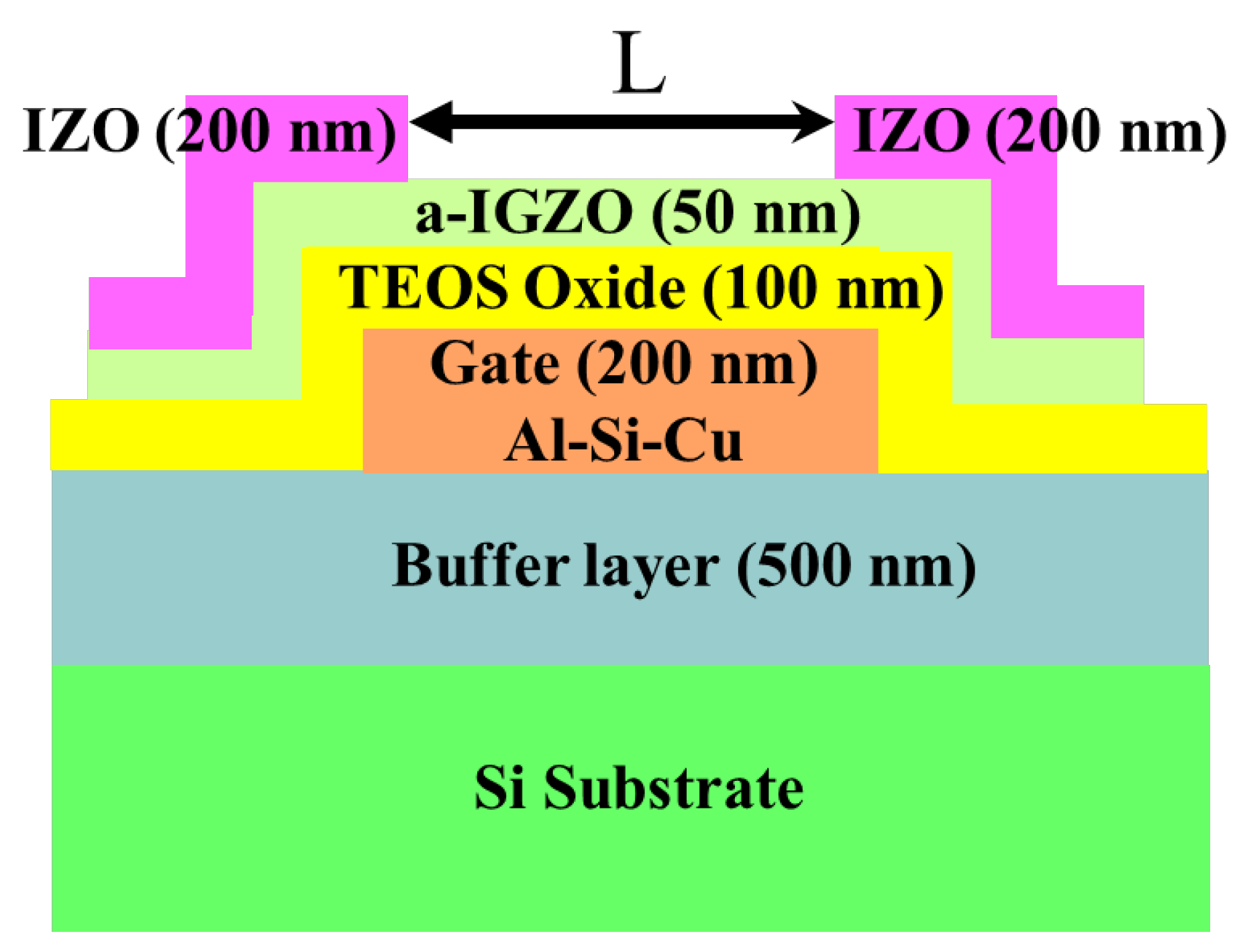
2.2. Thin-Film Transistor Fabrication and Characterization Measurements

In this study, an inverted-staggered thin-film transistor (TFT) structure was employed for the fabrication of a-IGZO TFT devices. A schematic cross-sectional view of the device is shown in Figure 1. Detailed fabrication procedures are described elsewhere [25]. The IGZO active layer, with a thickness of 50 nm, was deposited at room temperature via RF magnetron sputtering using a target with an atomic composition of In2O3:Ga2O3:ZnO = 1:1:2. The sputtering process was carried out at a constant power of 75 W, with Ar/O2 gas flow rates maintained at 50/1 sccm. The system’s background pressure and processing pressure were 5.3 × 10⁻⁴ Pa and 0.67 Pa, respectively. The sputtering power of the IZO films and the annealing temperatures in an N2 atmosphere at the end of the device fabrication were varied to investigate the effects of IZO films as source and drain electrodes on the electrical properties of IGZO TFTs. The devices were annealed at 200 °C, 300 °C, and 400 °C under the same working pressure, N2 flow rate, and duration as used for the IZO film conditions. Electrical measurements were carried out using an Agilent 4156A precision semiconductor parameter analyzer (Santa Clara, CA, USA) at a controlled temperature of 25 °C. For the transfer characteristics (IDS-VGS), VGS was varied from −10 V to + 20 V in 0.3 V steps for VDS = 0.1 V and 10 V, respectively. The calculation methods for µFE and the subthreshold swing (S.S.) are detailed in a previous study [26]. For the output characteristics (IDSVDS), VDS was varied from 0 V to + 20 V in 0.2 V steps for VGSVth = 5–11 V in the tested devices. The channel width (W) was fixed at 400 µm, and the designed channel length (L), defined as the distance between the source and drain metal pads, was varied from 10 µm to 100 µm. For a low VDS (0.1 V), Rtotal as a function of the designed L was evaluated using the total resistance method, applied within the linear region of the device’s output characteristics [24,25].
R t o t a l = V D S I D S = R c h + R S D = r c h L L + R S D
r c h = 1 μ E C O X W ( V G S V t h )
where rch denotes the channel resistance per channel length; RCH and RSD represent the channel resistance and the S–D contact resistance, respectively; Cox is the oxide capacitance per unit area; W is the channel width and L is the designed channel length, with ∆L = LLeff, where Leff is the effective channel length; the threshold voltage (Vth) is defined as the VGS at which the drain current (IDS) reaches a fixed value of 10−9 × (W/L) A; and µE represents the effective mobility. Further details about the total resistance method can be found in a previous study [25].

3. Results and Discussion

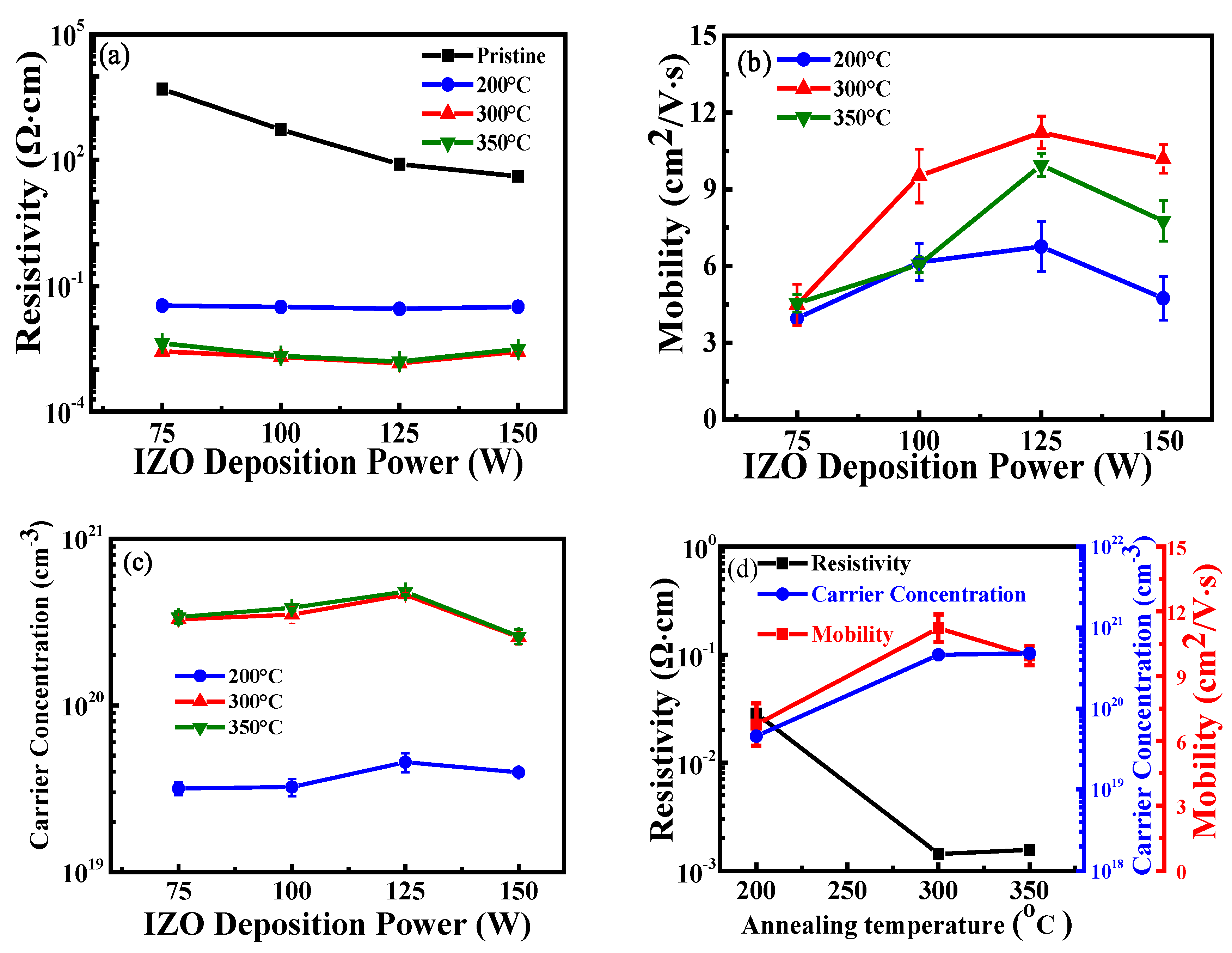
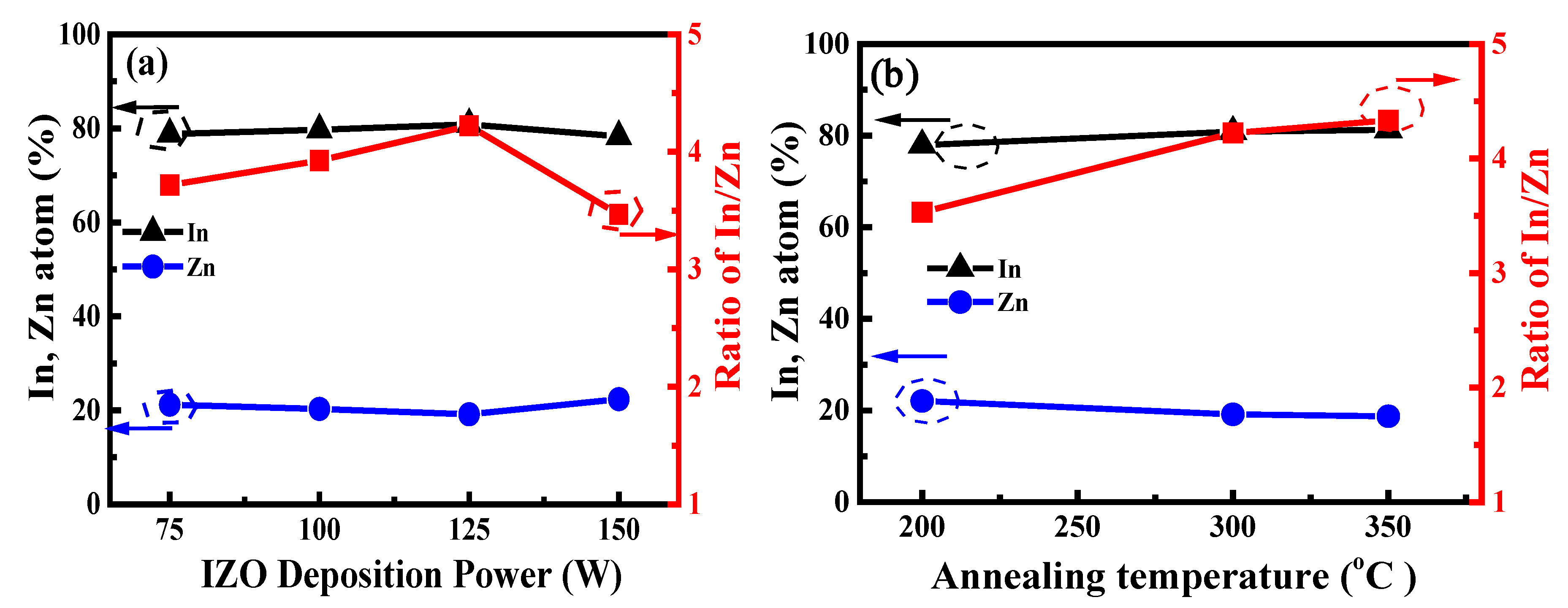
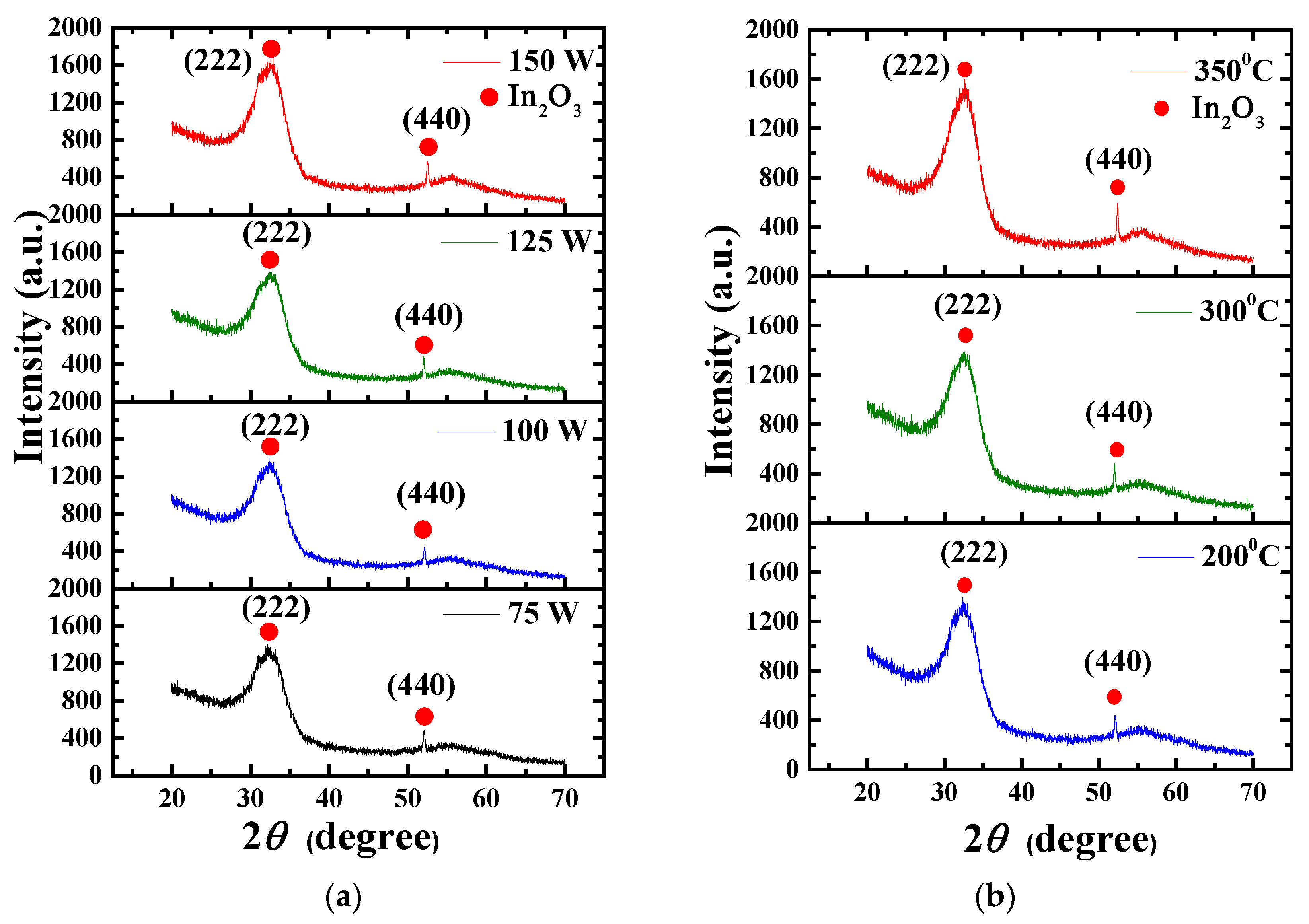
3.1. Properties of IZO Films at Various Sputtering Powers and Annealing Temperatures

Figure 2a,b show the transmittance spectra and optical bandgap of IZO films deposited with different sputtering powers and annealed at 300 °C, respectively. In this study, we carefully adjusted the deposition time to control the thickness of the IZO films in the range of 199–205 nm at various sputtering powers, based on the deposition rate of our RF sputtering system. The effect of thickness variation on the average transmittance (Tavg) was not significant due to the thickness variation being less than 5% in this study. As the sputtering power increased, the transmittance spectra of IZO thin films shifted toward longer wavelengths. Figure 2a shows that Tavg in the wavelength range of 400 to 800 nm for IZO films deposited at 125 W and annealed at 300 °C increased to 82.57%, whereas the Tavg of IZO films deposited at 150 W slightly decreased to 81.59%. In a direct bandgap semiconductor, the absorption coefficient (α) and the optical bandgap (Eg) can be estimated using the standard Tauc plot method from the optical transmission spectra, as described in references [27,28]:
( α h ν ) 2 = B h ν E g
α = 2.303 l o g 1 T d ; h v = h c / λ
where B is a material-dependent constant, λ is the wavelength of the incident photon, is the photon energy, T is the transmittance, and d is the thickness of the IZO films. According to the combined Equations (3) and (4), a plot is created with the y-axis representing (αhν)2 and the x-axis representing . After generating the curve based on the above data, a linear regression is performed using the last five data points. The intercept of the fitted line with the x-axis corresponds to the optical bandgap (Eg) of the IZO films at various sputtering powers after annealing in N2 at 300 °C, as shown in Figure 2b. The Eg values of the IZO films deposited at powers of 75, 100, 125, and 150 W and annealed at 300 °C were 3.19, 3.29, 3.37, and 3.24 eV, respectively. When the sputtering power increased from 75 W to 125 W, the optical bandgap increased from 3.19 eV to 3.37 eV; however, the optical bandgap of the IZO film deposited at 150 W decreased to 3.24 eV.
Figure 3a–c depict the Hall resistivity, carrier mobility, and carrier concentration of IZO films at different sputtering powers and various annealing temperatures. For the pristine IZO films, the resistivity was too high for Hall measurements and was therefore measured using a four-point probe method. As the sputtering power increased from 75 W to 125 W, the resistivity of the IZO films gradually decreased, while carrier mobility and carrier concentration increased. However, the resistivity of IZO films deposited at 150 W showed a slight increase, while both carrier mobility and carrier concentration significantly decreased. Figure 3d shows the Hall characteristics of IZO films deposited at 125 W under different annealing temperatures. As the annealing temperature increased from room temperature to 300 °C, the resistivity of the IZO films significantly decreased, while carrier mobility reached its maximum at 125 W, and carrier concentration peaked at 350 °C. However, when the annealing temperature reached 350 °C, the resistivity showed a slight increase, and carrier mobility slightly decreased. Therefore, the optimal electrical properties for IZO films were achieved at a sputtering power of 125 W and an annealing temperature of 300 °C, resulting in a resistivity of 1.73 × 10⁻³ Ω·cm, a carrier mobility of 11.12 cm2/V·s, and a carrier concentration of 4.61 × 1020 cm−3. It is worth mentioning that the resistivity of a-IGZO films at room temperature and annealing temperatures of 200 °C, 300 °C, and 400 °C were 1.25 × 10⁴, 7.81 × 10³, 0.218, and 2.10 × 10⁻² Ω·cm, respectively, as measured by the four-point probe. As the annealing temperature increases, the resistivity of the a-IGZO film gradually decreases.
Figure 4a shows the In, Zn, and resulting In/Zn atomic ratios of IZO films deposited at various powers and annealed at 300 °C. When the sputtering power increased from 75 W to 125 W, the indium (In) atomic percentage increased, whereas the zinc (Zn) atomic percentage decreased, resulting in a clear increase in the In/Zn ratio from 3.72 to 4.22. However, when the sputtering power reached 150 W, the In atomic percentage decreased, while the Zn atomic percentage increased, resulting in an abrupt decrease in the In/Zn ratio of 3.47 in the film. Figure 4b shows the In, Zn, and resulting In/Zn ratios in the films deposited at 125 W as a function of annealing temperature. The results were obtained using the EDS technique. While the comparison was only relative across different conditions, it clearly demonstrated that the In, Zn, and resulting In/Zn atomic ratios in the deposited films could be effectively controlled by adjusting the sputtering power of the IZO target and the annealing temperature. As the annealing temperature increased from 200 °C to 350 °C, the In atomic percentage continued to increase, while the Zn atomic percentage steadily decreased, leading to a continuous increase in the In/Zn ratio from 3.53 to 4.33, as shown in Figure 4b. Therefore, the In/Zn ratio in IZO films reached its maximum value of 4.33 at a sputtering power of 125 W and an annealing temperature of 350 °C. Figure 4a,b shows that the trend of the In/Zn ratio changed with increasing sputtering power and annealing temperature, respectively—a trend consistent with the carrier concentration variation shown in Figure 3c,d. These results indicate that the carrier concentration of the IZO film is related to the In/Zn ratio in the composition of the film. Sufficient doping of In3⁺ with Zn2⁺ in IZO films promotes the formation of oxygen vacancies. These vacancies are considered the primary source of the n-type free electrons in the film [21,29,30], leading to an increase in carrier concentration.
Figure 5a,b show the XRD crystalline phase analysis of IZO thin films at an annealing temperature of 300 °C with different sputtering powers and at a sputtering power of 125 W with different annealing temperatures, respectively. The crystalline phase analysis of the IZO thin film was conducted using GIXRD. The peak positions of In2O3 include a broad amorphous peak corresponding to the (222) plane at approximately 2θ ≈ 32.0–32.6° and a distinctive peak corresponding to the strongest crystalline plane, (440), at 2θ ≈ 52.0–52.5°, as indicated by JCPDS No. 76-0152. These peaks are observed in the diffraction patterns of IZO films, as shown in Figure 5a,b. The average grain size (D) was estimated from the full width at half maximum (FWHM) of the In2O3 (440) diffraction peak using the Scherrer equation [31].
D = 0.9λ/βcosθ
where λ is the X-ray wavelength (λ = 0.15418 nm), θ is the Bragg diffraction angle, and β is the full width at half maximum (FWHM) of the diffraction peak, expressed in radians. Using Equation (5), the average grain sizes (D values) of IZO films annealed at 300 °C were calculated to be 31, 34, 55, and 40 nm for sputtering powers of 75, 100, 125, and 150 W, respectively. As shown in Figure 6, the D values were 34, 55, and 44 nm at annealing temperatures of 200, 300, and 350 °C, respectively. The IZO film deposited at 125 W and annealed at 300 °C exhibited the largest grain size, which corresponded to the highest carrier mobility, as shown in Figure 3b. Furthermore, as shown in Figure 3d, carrier mobility increased with annealing temperature from 200 °C to 300 °C, attributed to grain growth and the corresponding reduction in grain boundary scattering. However, a further increase in annealing temperature to 350 °C resulted in decreased mobility, likely due to enhanced grain boundary and ionized impurity scattering. These results indicate that optimizing sputtering power and annealing temperature can effectively control the crystallinity of the In2O3 (440) phase and minimize grain boundary scattering in IZO films.
To explain the effects of different sputtering powers on the IZO film’s optical and electrical properties, the surface roughness of the film was further analyzed. A 500 nm SiO2 film was deposited on a silicon substrate, with an RMS roughness of 4.2 nm and an Ra of 3.21 nm, serving as the substrate layer for the AFM sample. Figure 6a–d show AFM images, RMS roughness, and Ra average roughness of IZO films deposited at different powers annealed at 300 °C. At 300 °C annealing, when the IZO sputtering power increased from 75 W to 125 W, the surface roughness RMS decreased from 5.2 nm to 4.66 nm and the Ra decreased from 4.02 nm to 3.66 nm, respectively. However, at a sputtering power of 150 W, the surface roughness in terms of RMS and Ra slightly increased to 4.8 nm and 3.91 nm, respectively. From the AFM surface roughness results of the IZO film, as the sputtering power increased from 75 W to 125 W, the surface roughness significantly decreased, leading to an increase in carrier mobility from 4.49 to 11.12 cm2/V·s. However, when the sputtering power increased to 150 W, the slight increase in surface roughness caused the carrier mobility to decrease to 10.2 cm2/V·s. The trends of RMS and Ra surface roughness of the IZO films as a function of sputtering power show an inverse relationship with the average grain size estimated using the Scherrer equation. Ku et al. [19] reported that the mobility values of the IZO films deposited with oxygen contents of 0.5% and 1.0% decreased upon crystallization, whereas those deposited with 0.25% oxygen content continued to increase. These differences arise from variations in their crystalline structures, specifically the presence of the In2O3 crystalline phase in the crystallized films. From the optical transmittance spectrum results in Figure 2a, at a sputtering power of 150W, the increase in surface roughness also caused a slight decrease in average transmittance. In summary, the composition and microstructure of the IZO film have a significant impact on the optical and electrical properties of the transparent conductive film.
The effects of sputtering power and annealing temperature of IZO films, used as source and drain electrodes, on the electrical characteristics of a-IGZO TFTs are discussed in the following sections.

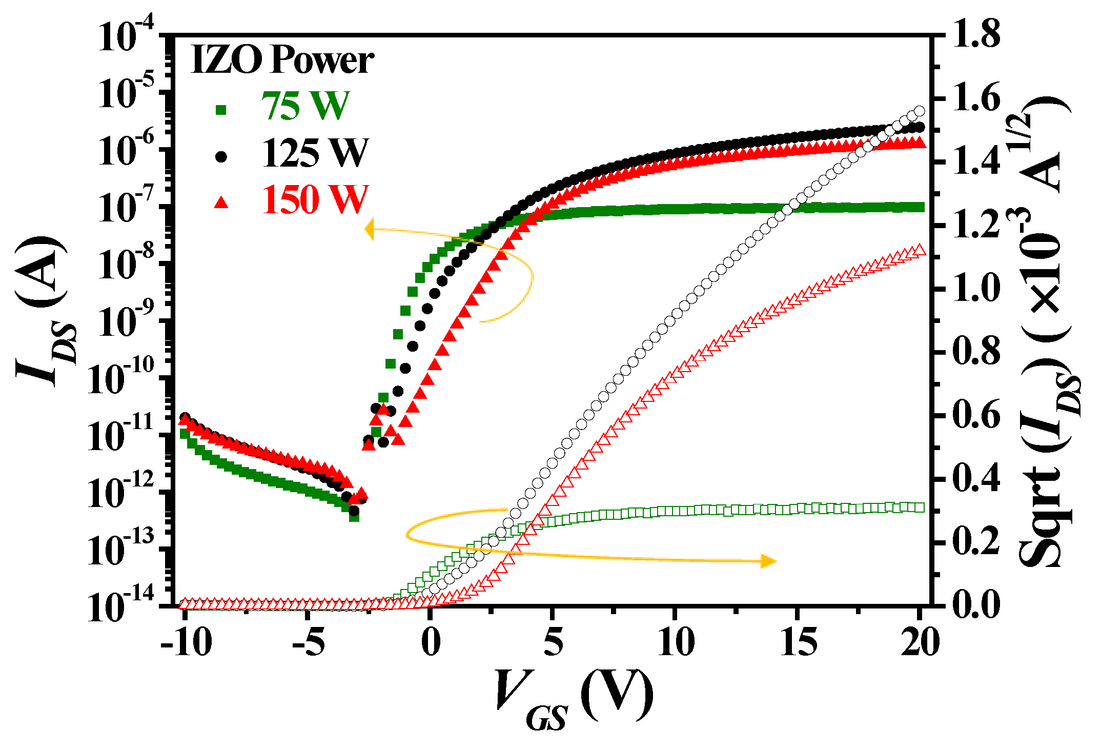
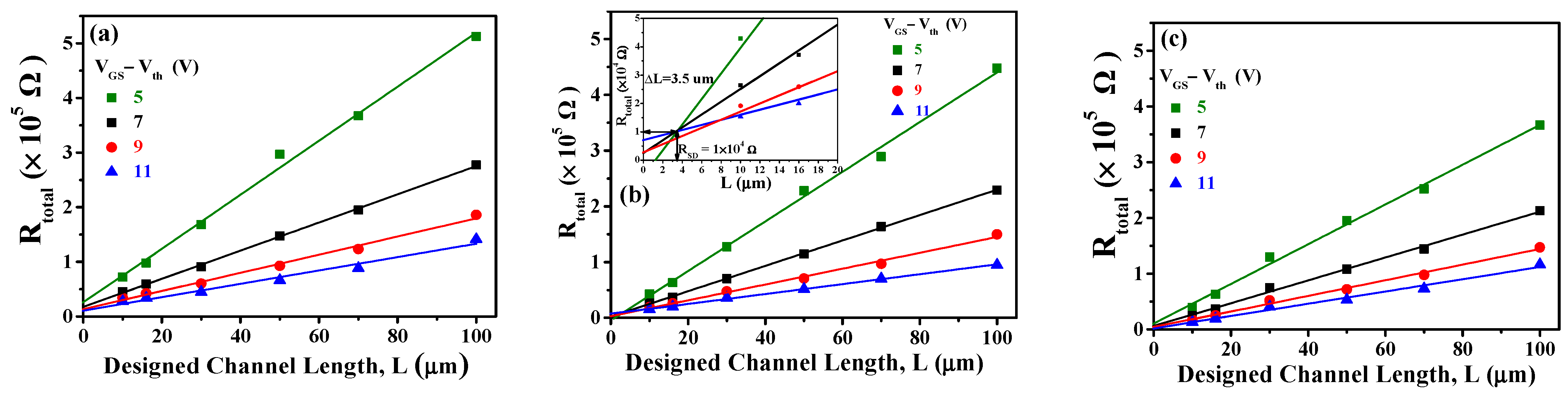
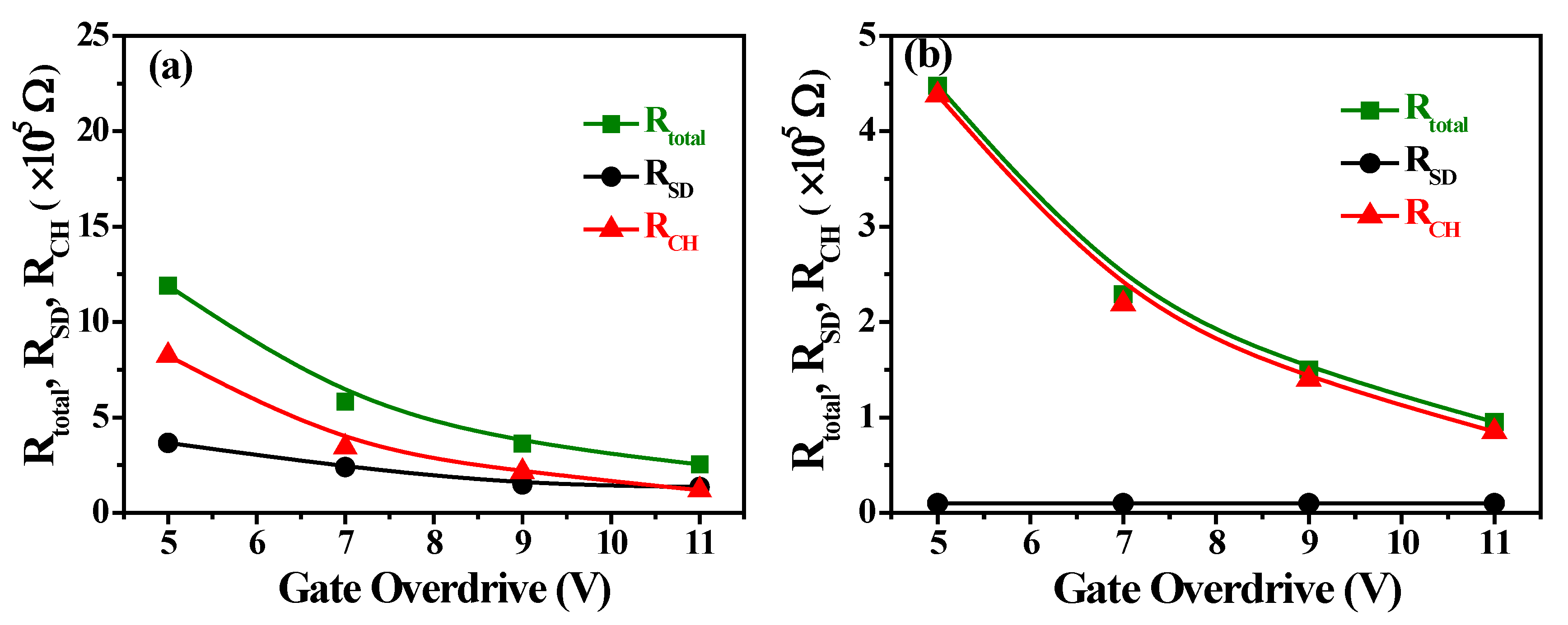
3.2. Electrical Characteristics of A-IGZO TFTs Using IZO Films as S–D Electrodes with Various Deposition Powers

Figure 7 shows the IDS-VGS and IDS1/2-VGS transfer characteristic curves of a-IGZO TFTs at W/L = 400/100 μm and an annealing temperature of 300 °C with IZO as the S/D electrodes deposited at different powers characterized at VDS = 0.1 V. Measurements were conducted on more than three samples per device. The gate capacitance per unit area (Cox) of the 100 nm TEOS oxide was measured to be 4.98 × 10⁻⁸ F/cm2. Table 1 presents the average values and standard deviations of the extracted electrical parameters of a-IGZO TFTs with IZO electrodes deposited at varying powers. The subthreshold swing (SS) value approximately doubles, ranging from ~0.62 to ~1.22 V/decade as the sputtering power increases. This is due to the increased deep-level defects in the a-IGZO channel layer caused by Ar ion bombardment [23]. Additionally, Vth, ranging from ~−0.24 to ~2.11 V, and the tangent voltage of the IDS1/2 vs. VGS curve shift toward more positive values, which is related to the increase in deep-level defects within the channel layer and interface defects at the dielectric layer. The field-effect mobility (μFE) (~12.31 cm2/V·s) and the on current (~2.09 × 10⁻⁶ A) reach their maximum values at a sputtering power of 125 W. This is attributed to the highest In/Zn atomic ratio observed at 125 W, which leads to an increase in the carrier concentration of the IZO films, as shown in Figure 3c. In addition, the largest average grain size (D) and the lowest RMS roughness at 125 W result in the highest carrier mobility, as shown in Figure 3b. Consequently, these factors contribute to the lowest film resistivity of the IZO films at 125 W, as shown in Figure 3a. However, the IZO films deposited at 150 W exhibit lower carrier mobility and carrier concentration, leading to higher film resistivity, as shown in Figure 3a–c, and resulting in a slight decrease in μFE (~9.89 cm2/V·s) and on-current (Ion, ~1.82 × 10⁻⁶ A) of the a-IGZO TFTs.
Figure 8a–c show the IDS-VDS output characteristic curves of a-IGZO TFTs at W/L = 400/100 μm and an annealing temperature of 300 °C with IZO as the S/D electrodes deposited at different powers characterized at various gate overdrive VGSVth = 5–11 V. When VGSVth = 11 V and the IZO sputtering powers are 75 W, 125 W, and 150 W, the corresponding saturation drain currents are approximately 2.88 × 10⁻⁵, 4.09 × 10⁻⁵, and 3.90 × 10⁻⁵A, respectively. From the IDS-VDS curves, it can be observed that the saturation current no longer increases for a power of 125 W. This result may be attributed to the higher In/Zn ratio and carrier concentration (~5.77 × 1020 cm−3) in the IZO film at 125W, as shown in Figure 4a and Figure 3c, respectively. Figure 9a–c show the relationship between Rtotal and different channel lengths (R-L plots) for a-IGZO TFT devices (W = 400 μm) with IZO deposited at different powers and annealed at 300 °C characterized at VDS = 0.1 V and VGSVth = 5–11 V. Using Equation (1), the Rtotal, RSD, and RCH values for each channel length can be extracted (where ΔL = 0 μm for 75 W and 150 W). Additionally, for the 125 W power condition, an intersection appears when applying the total resistance method, yielding RSD = 1 × 10⁴ Ω, ΔL = 3.5 μm, as shown in the inset of Figure 9b. The channel length shrinkage, ΔL = 3.5 μm, can be attributed to the critical-dimension loss of the S/D electrode spacing, which occurs during the lithographic and subsequent lift-off process steps. Figure 10a–c show the extracted Rtotal, RCH, and RSD at various gate overdrives for a-IGZO TFTs with IZO electrodes (L = 100 μm) deposited at powers of 75 W, 125 W, and 150 W and annealed at 300 °C. Based on the R–L plots in Figure 9, with a W/L ratio of 400/100 μm and a gate overdrive of 9 V, increasing the sputtering power from 75 W to 150 W results in a slight decrease in RCH from 1.73 × 10⁵ Ω to 1.43 × 10⁵ Ω, while RSD decreases significantly from 1.32 × 10⁴ Ω to 3.93 × 10³ Ω. This improvement is attributed to the reduced resistivity of the IZO films at higher sputtering powers, as shown in Figure 3a. IZO films deposited at higher powers exhibit larger average grain sizes (Figure 5) and lower RMS surface roughness (Figure 6), which in turn reduce RSD at the interface between the IZO electrodes and the a-IGZO channel layer. According to Equation (1) at VGSVth = 11 V, as the sputtering power increases from 75 W to 125 W, RCH decreases from 1.30 × 10⁴ Ω to 8.50 × 10³ Ω. However, at 150 W, RCH increases to 1.14 × 10⁴ Ω. Since RCH reaches its lowest value at a sputtering power of 125 W across all gate overdriving voltages, Equation (2) indicates that this results in the highest effective mobility (μE). Based on these electrical characteristics, the optimal sputtering power for IZO source–drain electrodes in a-IGZO TFTs is determined to be 125 W.

3.3. Electrical Characteristics of A-IGZO TFTs Determined by Using IZO Films as S–D Electrodes with Various Annealing Temperatures

Figure 11 shows the IDS-VGS and IDS1/2-VGS transfer characteristics of a-IGZO TFTs at VDS = 0.1 V and W/L = 400/100 μm with IZO as the S–D electrodes deposited at a power of 125 W and annealed at different temperatures in ambient N2. Table 2 shows the extracted parameters of a-IGZO TFT devices with IZO electrodes deposited at a power of 125 W and annealed at different temperatures. As the annealing temperature increases from the pristine state to 300 °C, the S.S. value decreases by approximately half (from 1.88 to 0.85 V/decade), while the μFE value increases from 4.71 to 12.31 cm2/V·s and the on current rises from 4.69 × 10⁻⁷ to 2.09 × 10⁻⁶ A. This improvement is due to high-temperature annealing, which significantly improves the interface between the a-IGZO channel layer and the dielectric layer, reducing thin-film trap defects and increasing film density [32]. Additionally, the threshold voltage decreases from 6.6 to 0.33 V, and the IDS1/2 vs. VGS curve clearly shows a shift in the tangent voltage toward a more negative voltage. This shift is attributed to high-temperature annealing, which increases the carrier concentration in the a-IGZO channel layer and decreases the film resistivity. Furthermore, annealing at 400 °C leads to depletion-mode TFTs due to the excessively low channel resistivity (2.10 × 10⁻² Ω·cm) of a-IGZO films, as measured by the four-point probe, and the higher Ioff current (8.65 × 10⁻⁶ A). As a result, the Vth, SS, and μFE parameters cannot be determined.
To establish the relationship between IZO S–D electrodes annealed at different temperatures and device performance, the output characteristics of devices with varying channel lengths (L) were analyzed using the total resistance method. From the R–L plots for a-IGZO TFT devices (W = 400 μm) with IZO as the S–D electrodes annealed at different temperatures, characterized at VDS = 0.1 V and VGSVth = 5–11 V, the Rtotal, RSD, and RCH values for each channel length can be extracted using Equation (1). Figure 12a,b show the Rtotal, RSD, and RCH plots at different gate overdrive voltages for IGZO TFTs with IZO as the S–D electrodes annealed at 200 °C and 300 °C, respectively. The source–drain contact resistance (RSD) decreases significantly—by nearly an order of magnitude—as the annealing temperature increases from 200 °C to 300 °C. This result is attributed to the increased carrier concentration and mobility in the IZO film with rising annealing temperature, as shown in Figure 3d, which leads to a marked reduction in both film resistivity and RSD. Furthermore, as the annealing temperature increases from 200 °C to 300 °C, both Rtotal and RCH decrease significantly by a factor of 2 to 3. This is due to the reduced resistivity of the IZO film, as illustrated in Figure 3d, and the substantial decrease in the resistivity of the a-IGZO thin films—from 7.81 × 10³ to 0.218 Ω·cm. Therefore, the optimal annealing temperature for IZO as the source–drain electrodes in a-IGZO TFTs is 300 °C.

4. Conclusions

In summary, the optimal electrical performance of IZO thin films was achieved at a sputtering power of 125 W and an annealing temperature of 300 °C, where the films exhibited the lowest resistivity, the highest carrier mobility, and enhanced carrier concentration. These improvements are attributed to increased grain size, reduced surface roughness, and a favorable In/Zn atomic ratio. Further increases in sputtering power (to 150 W) or annealing temperature (to 350 °C) led to slight degradation in mobility and resistivity, likely due to increased grain boundary and ionized impurity scattering.
The μFE (~12.31 cm2/V·s) and the on current (~2.09 × 10⁻⁶ A) reach their maximum values at a sputtering power of 125 W. This is attributed to the highest In/Zn atomic ratio observed at 125 W, which leads to an increase in the carrier concentration of the IZO films. In addition, the largest average grain size and the lowest RMS roughness at 125 W result in the highest carrier mobility. Consequently, these factors contribute to the lowest film resistivity of the IZO films at 125 W. However, the IZO films deposited at 150 W exhibit lower carrier mobility and carrier concentration, leading to higher film resistivity, and resulting in a slight decrease in the μFE (~9.89 cm2/V·s) and on current (Ion, ~1.82 × 10⁻⁶ A) of the a-IGZO TFTs. According to the total resistance method, IZO films deposited at higher powers exhibit larger average grain sizes and lower RMS surface roughness, which in turn reduce RSD at the interface between the IZO electrodes and the a-IGZO channel layer. Additionally, RCH reaches its minimum value at a sputtering power of 125 W across all gate overdrive voltages, indicating that this results in the highest effective mobility (μE) in the channel. Based on these electrical characteristics, the optimal sputtering power for IZO source–drain electrodes in a-IGZO TFTs is determined to be 125 W.
As the annealing temperature increases from the pristine state to 300 °C, the SS value decreases by approximately half, while the μFE and Ion current gradually increase. This improvement is attributed to high-temperature annealing. The Vth clearly shifts toward negative voltage. The RSD decreases significantly—by nearly an order of magnitude—as the annealing temperature increases from 200 °C to 300 °C. This result is attributed to the increased carrier concentration and mobility in the IZO film with rising annealing temperature, which leads to a marked reduction in both film resistivity and RSD. Furthermore, as the annealing temperature increases from 200 °C to 300 °C, both Rtotal and RCH decrease significantly by a factor of 2 to 3. This is due to the reduced resistivity of the IZO film and the substantial decrease in the resistivity of the a-IGZO thin films. Therefore, 300 °C is identified as the optimal annealing temperature for IZO as the S–D electrodes in a-IGZO TFTs. Based on the analysis of electrical properties of a-IGZO TFTs with IZO source–drain electrodes, the optimal sputtering power and annealing temperature were determined to be 125 W and 300 °C, respectively.

Author Contributions

Conceptualization, Y.-S.L. and H.-C.L.; methodology, Y.-S.L. and H.-C.L.; software, C.-H.C., B.-S.L., V.-T.T.N. and T.-C.T.; validation, C.-H.C., B.-S.L. and V.-T.T.N.; formal analysis, C.-H.C., B.-S.L. and V.-T.T.N.; investigation, C.-H.C. and B.-S.L.; resources, Y.-S.L. and H.-C.L.; data curation, C.-H.C., B.-S.L. and V.-T.T.N.; writing—original draft preparation, Y.-S.L., C.-H.C. and B.-S.L.; writing—review and editing, Y.-S.L., C.-H.C. and B.-S.L.; visualization, T.-C.T.; funding acquisition, Y.-S.L. All authors have read and agreed to the published version of the manuscript.

Funding

This research was funded by the National Science and Technology Council under Projects NSTC 113-NU-E-159-001-NU and NSTC 114-NU-E-159-001-NU.

Data Availability Statement

The data presented in this study are available on request from the corresponding author.

Acknowledgments

The authors extend appreciation to the Taiwan Semiconductor Research Institute (TSRI) for supplying the SEM equipped with EDS systems. We gratefully acknowledge the use of the high-performance, low-temperature, and multi-function X-ray diffractometer belonging to the Core Facility Center of National Yang Ming Chiao Tung University.

Conflicts of Interest

The authors declare no conflicts of interest.

Abbreviations

The following abbreviations are used in this manuscript:
IZO S–DIn-Zn-O source-drain
a-IGZOamorphous In-Ga-Zn-O
TFTsthin-film transistors
Rtotaltotal resistance
RSDcontact resistance
RCHchannel resistance
µFEfield-effect mobility
Ionon-current
SSsubthreshold swing
Vththreshold voltage

References

  1. Ajayan, J.; Sreejith, S.; Kumari, N.A.; Manikandan, M.; Sen, S.; Kumar, M. Amorphous indium gallium zinc oxide thin film transistors (a-IGZO-TFTs): Exciting prospects and fabrication challenges. Microelectron. Eng. 2025, 298, 112327. [Google Scholar] [CrossRef]
  2. Ji, D.; Jang, J.; Park, J.H.; Kim, D.; Rim, Y.S.; Hwang, D.K.; Noh, Y.-Y. Recent progress in the development of backplane thin film transistors for information displays. J. Inf. Disp. 2023, 24, 159–168. [Google Scholar] [CrossRef]
  3. Lim, S.-H.; Mah, D.-G.; Cho, W.-J. Enhancing the Stability and Mobility of TFTs via Indium–Tungsten Oxide and Zinc Oxide Engineered Heterojunction Channels Annealed in Oxygen Ambient. Nanomaterials 2024, 14, 1252. [Google Scholar] [CrossRef] [PubMed]
  4. Zhao, M.; Yan, J.; Wang, Y.; Chen, Q.; Cao, R.; Xu, H.; Wuu, D.-S.; Wu, W.-Y.; Lai, F.-M.; Lien, S.-Y.; et al. The Enhanced Performance of Oxide Thin-Film Transistors Fabricated by a Two-Step Deposition Pressure Process. Nanomaterials 2024, 14, 690. [Google Scholar] [CrossRef]
  5. Park, J.-M.; Jang, S.C.; Lee, S.M.; Kang, M.-H.; Chung, K.-B.; Kim, H.-S. Oxide thin-film transistors based on i-line stepper process for high PPI displays. J. Inf. Disp. 2023, 24, 103–108. [Google Scholar] [CrossRef]
  6. Shimura, Y.; Nomura, K.; Yanagi, H.; Kamiya, T.; Hirano, M.; Hosono, H. Specific contact resistances between amorphous oxide semiconductor In–Ga–Zn–O and metallic electrodes. Thin Solid Film. 2008, 516, 5899–5902. [Google Scholar] [CrossRef]
  7. Barquinha, P.; Vilà, A.M.; Gonçalves, G.; Pereira, L.; Martins, R.; Morante, J.R.; Fortunato, E. Gallium–Indium–Zinc-Oxide-Based Thin-Film Transistors: Influence of the Source/Drain Material. IEEE Trans. Electron Devices 2008, 55, 954–960. [Google Scholar] [CrossRef]
  8. Choi, S.-H. High-Performance Oxide TFTs With Co-Sputtered Indium Tin Oxide and Indium-Gallium-Zinc Oxide at Source and Drain Contacts. IEEE Electron. Device Lett. 2021, 42, 168–171. [Google Scholar] [CrossRef]
  9. Li, Q.; Han, D.; Don, J.; Xu, D.; Li, Y.; Wang, Y.; Zhang, X. Effects of Source/Drain Electrodes on the Performance of InSnO Thin-Film Transistors. Micromachines 2022, 13, 1896. [Google Scholar] [CrossRef]
  10. Tappertzhofen, S. Impact of electrode materials on the performance of amorphous IGZO thin-film transistors. MRS Adv. 2022, 7, 723–728. [Google Scholar] [CrossRef]
  11. Pain, D.C.; Yaglioglu, B.; Beiley, Z.; Lee, S. Amorphous IZO-based transparent thin film transistors. Thin Solid Film. 2008, 516, 5894–5898. [Google Scholar] [CrossRef]
  12. Barquinha, P.; Gonçalves, G.; Pereira, L.; Martins, R.; Fortunato, E. Effect of annealing temperature on the properties of IZO films and IZO based transparent TFTs. Thin Solid Film. 2007, 515, 8450–8454. [Google Scholar] [CrossRef]
  13. Yaglioglu, B.; Yeom, H.Y.; Beresford, R.; Painea, D.C. High-mobility amorphous In2O3–10wt%ZnO thin film transistors. Appl. Phys. Lett. 2006, 89, 062103. [Google Scholar] [CrossRef]
  14. Sung, S.-Y.; Choi, J.H.; Han, U.B.; Lee, K.C.; Lee, J.-H.; Kim, J.-J.; Lim, W.; Pearton, S.J.; Norton, D.P.; Heo, Y.-W. Effects of ambient atmosphere on the transfer characteristics and gate-bias stress stability of amorphous indium-gallium-zinc oxide thin-film transistors. Appl. Phys. Lett. 2010, 96, 102107. [Google Scholar] [CrossRef]
  15. Jeong, J.K.; Jeong, J.H.; Yang, H.W.; Park, J.-S.; Mo, Y.-G.; Kim, H.D. High performance thin film transistors with cosputtered amorphous indium gallium zinc oxide channel. Appl. Phys. Lett. 2007, 91, 113505. [Google Scholar] [CrossRef]
  16. Jeon, S.; Ahn, S.-E.; Song, I.; Jeon, Y.; Kim, Y.; Kim, S.; Choi, H.; Kim, H.; Lee, E.; Lee, S.; et al. Dual gate photo-thin film transistor with high photoconductive gain for high reliability, and low noise flat panel transparent imager. In Proceedings of the International Electron Devices Meeting, Washington, DC, USA, 5–7 December 2011. [Google Scholar]
  17. Kim, S.I.; Kim, C.J.; Park, J.; Song, I.; Kim, S.W.; Yin, H.; Lee, E.; Lee, J.C.; Park, Y. High Performance Oxide Thin Film Transistors with Double Active Layers. In Proceedings of the International Electron Devices Meeting, San Francisco, CA, USA, 15–17 December 2008. [Google Scholar]
  18. Hong, S.; Lee, S.; Mativenga, M.; Jang, J. Reduction of Negative Bias and Light Instability of a-IGZO TFTs by Dual-Gate Driving. IEEE Electron. Device Lett. 2014, 35, 93–95. [Google Scholar] [CrossRef]
  19. Ku, D.Y.; Kim, I.H.; Lee, I.; Lee, K.S.; Lee, T.S.; Jeong, J.-h.; Cheong, B.; Baik, Y.-J.; Kim, W.M. Structural and electrical properties of sputtered indium–zinc oxide thin films. Thin Solid Film. 2006, 515, 1364–1369. [Google Scholar] [CrossRef]
  20. Gonçalves, G.; Elangovan, E.; Barquinha, P.; Pereira, L.; Martins, R.; Fortunato, E. Influence of post-annealing temperature on the properties exhibited by ITO, IZO and GZO thin films. Thin Solid Film. 2007, 515, 8562–8566. [Google Scholar] [CrossRef]
  21. Jung, Y.S.; Seoa, J.Y.; Leea, D.W.; Jeon, D.Y. Influence of DC magnetron sputtering parameters on the properties of amorphous indium zinc oxide thin film. Thin Solid Film. 2003, 445, 63–71. [Google Scholar] [CrossRef]
  22. Lee, C.; Lee, W.; Kim, H.; Kim, H.W. Influence of annealing atmosphere on the structure, resistivity and transmittance of InZnO thin films. Ceram. Int. 2008, 34, 1089–1092. [Google Scholar] [CrossRef]
  23. Lim, W.; Wang, Y.-L.; Renb, F.; Norton, D.P.; Kravchenko, I.I.; Zavada, J.M.; Pearton, S.J. Indium zinc oxide thin films deposited by sputtering at room temperature. Appl. Surf. Sci. 2008, 254, 2878–2881. [Google Scholar] [CrossRef]
  24. Sato, A.; Abe, K.; Hayashi, R.; Kumomi, H.; Nomura, K.; Kamiya, T.; Hirano, M.; Hosono, H. Amorphous In–Ga–Zn–O coplanar homojunction thin-film transistor. Appl. Phys. Lett. 2009, 94, 133502. [Google Scholar] [CrossRef]
  25. Lee, Y.-S.; Yen, T.-W.; Lin, C.-I.; Lin, H.-C.; Yeh, Y. Electrical characteristics of amorphous In–Ga–Zn–O thin-film transistors prepared by radio frequency magnetron sputtering with varying oxygen flows. Displays 2014, 35, 165–170. [Google Scholar] [CrossRef]
  26. Lee, Y.-S.; Wang, Y.-H.; Tien, T.-C.; Hsieh, T.-E.; Lai, C.-H. Electrical Characteristics and Stability Improvement of Top-Gate In-Ga-Zn-O Thin-Film Transistors with Al2O3/TEOS Oxide Gate Dielectrics. Coatings 2020, 10, 1146. [Google Scholar] [CrossRef]
  27. Tang, Z.K.; Wong, G.K.L.; Yu, P.; Kawasaki, M.; Ohtomo, A.; Koinuma, H.; Segawa, Y. Room-temperature ultraviolet laser emission from self-assembled ZnO microcrystallite thin films. Appl. Phys. Lett. 1998, 72, 3270–3272. [Google Scholar] [CrossRef]
  28. Minegishi, K.; Koiwai, Y.; Kikuchi, Y. Growth of p-type Zinc Oxide Films by Chemical Vapor Deposition. Jpn. J. Appl. Phys. 1997, 36, L1453. [Google Scholar] [CrossRef]
  29. Lei, P.; Yan, X.C.Y.; Peng, J.; Hao, C.; Ji, J.; Huo, Z. Transparent and conductive IZO films: Oxygen and discharge voltage controlled sputtering growth and properties. Vacuum 2022, 195, 110645. [Google Scholar] [CrossRef]
  30. Naghavi, N.; Marcel, C.; Dupont, L.; Rougier, A.; Leriche, J.-B.; Guery, C. Structural and physical characterisation of transparent conducting pulsed laser deposited In2O3–ZnO thin films. J. Mater. Chem. 2000, 10, 2315–2319. [Google Scholar] [CrossRef]
  31. Song, D.; Windenborg, P.; Chin, W.; Aberle, A. Investigation of lateral parameter variations of Al-doped zinc oxide films prepared on glass substrates by RF magnetron sputtering. Sol. Energy Mater. Sol. Cells 2002, 73, 1–20. [Google Scholar] [CrossRef]
  32. Barquinha, P.; Pereira, L.; Gonçalves, G.; Martins, R.; Fortunato, E. The effect of deposition conditions and annealing on the performance of high-mobility GIZO TFTs. Electrochem. Solid-State Lett. 2008, 11, H248–H251. [Google Scholar] [CrossRef]
Figure 1. Cross-sectional diagram of the fabricated a-IGZO TFT devices.
Nanomaterials 15 00780 g001
Figure 2. (a) Transmittance and (b) optical bandgap of IZO films deposited at different sputtering powers after annealing in N2 at 300 °C.
Nanomaterials 15 00780 g002
Figure 3. (a) Resistivity, (b) carrier mobility, and (c) carrier concentration of IZO films as a function of sputtering power at different annealing temperatures; (d) Hall characteristic of IZO films deposited at 125 W under different annealing temperatures.
Nanomaterials 15 00780 g003
Figure 4. In, Zn, and resulting In/Zn atomic ratios of IZO films (a) deposited at various powers and annealed at 300 °C and (b) deposited at 125 W as a function of annealing temperature.
Nanomaterials 15 00780 g004
Figure 5. XRD crystalline phase analysis of IZO films: (a) at an annealing temperature of 300 °C with different sputtering powers and (b) at a sputtering power of 125 W with different annealing temperatures.
Nanomaterials 15 00780 g005
Figure 6. AFM images, RMS roughness, and Ra average roughness of IZO films deposited at (a) 75 W, (b) 100 W, (c) 125 W, and (d) 150 W after annealing at 300 °C.
Nanomaterials 15 00780 g006
Figure 7. IDS-VGS and IDS1/2-VGS transfer characteristic curves of a-IGZO TFTs at VDS = 0.1 V and W/L = 400/100 μm with IZO as the S/D electrodes deposited at different powers.
Nanomaterials 15 00780 g007
Figure 8. IDS-VDS output characteristic curves of a-IGZO TFTs (W/L = 400/100 μm) with IZO as the S/D electrodes deposited at sputtering powers of (a) 75 W, (b) 125 W, and (c) 150 W.
Nanomaterials 15 00780 g008
Figure 9. Dependences of Rtotal on the designed L of a-IGZO TFTs with IZO electrodes at different powers: (a) 75 W, (b) 125 W, and (c) 150 W. The inset provides a magnified view of the small L to highlight the point of intersection.
Nanomaterials 15 00780 g009
Figure 10. Gate overdrive dependence of Rtotal, RSD, and RCH for a-IGZO TFTs with IZO electrodes annealed at 300 °C under different sputtering powers: (a) 75 W, (b) 125 W, and (c) 150 W.
Nanomaterials 15 00780 g010
Figure 11. IDS-VGS and IDS1/2-VGS transfer characteristics of a-IGZO TFTs at VDS = 0.1 V and W/L = 400/100 μm with IZO as the S–D electrodes annealed at different temperatures.
Nanomaterials 15 00780 g011
Figure 12. Rtotal, RSD, and RCH plots at different gate overdrive voltages for IGZO TFTs (W/L = 400/100 μm) with IZO as the S–D electrodes at (a) 200 °C and (b) 300 °C.
Nanomaterials 15 00780 g012
Table 1. Extracted electrical parameters of a-IGZO TFTs at VDS = 0.1 V and W/L = 400/100 μm with IZO electrodes at different sputtering powers.
Power (W)Vth (V)S.S. (V/decade)μFE (cm2/V·s)Ion (A)Ioff (A)
75−0.24 ± 0.170.62 ± 0.115.51 ± 0.405.92 × 10−73.7 × 10⁻¹³
1250.33 ± 0.040.85 ± 0.0612.31 ± 0.392.09 × 10−67.6 × 10⁻¹³
1502.11 ± 0.221.22 ± 0.059.89 ± 0.981.82 × 10−67.1 × 10⁻¹³
Table 2. Extracted parameters of a-IGZO TFT devices with IZO electrodes annealed at different temperatures.
Tanneal (°C)Vth (V)S.S. (V/decade)μFE (cm2/V·s)Ion (A)Ioff (A)
Pristine6.6 ± 0.011.88 ± 0.164.71 ± 0.044.69 × 10−74 × 10−13
2004.08 ± 0.071.39 ± 0.036.20 ± 0.028.76 × 10−74.5 × 10⁻¹³
3000.33 ± 0.040.85 ± 0.0612.31 ± 0.392.09 × 10−67.6 × 10⁻¹³
400NANANA2.8 × 10−58.65 × 10⁻⁶
Disclaimer/Publisher’s Note: The statements, opinions and data contained in all publications are solely those of the individual author(s) and contributor(s) and not of MDPI and/or the editor(s). MDPI and/or the editor(s) disclaim responsibility for any injury to people or property resulting from any ideas, methods, instructions or products referred to in the content.

