Abstract
Vanadium dioxide (VO2) stands out for its versatility in numerous applications, thanks to its unique reversible insulator-to-metal phase transition. This transition can be initiated by various stimuli, leading to significant alterations in the material’s characteristics, including its resistivity and optical properties. As the interest in the material is growing year by year, the purpose of this review is to explore the trends and current state of progress on some of the applications proposed for VO2 in the field of sensors and actuators using literature review methods. Some key applications identified are resistive sensors such as strain, temperature, light, gas concentration, and thermal fluid flow sensors for microfluidics and mechanical microactuators. Several critical challenges have been recognized in the field, including the expanded investigation of VO2-based applications across multiple domains, exploring various methods to enhance device performance such as modifying the phase transition temperature, advancing the fabrication techniques for VO2 structures, and developing innovative modelling approaches. Current research in the field shows a variety of different sensors, actuators, and material combinations, leading to different sensor and actuator performance input ranges and output sensitivities.
1. Introduction
Vanadium dioxide (VO2) is a material that undergoes a reversible transition between metal and insulator states. Insulator–metal transition (IMT) occurs at a reasonably convenient temperature and can be further modified using doping. This property of VO2 was first discovered in 1959 [1] and has been the subject of ongoing research endeavors ever since. Areas of interest include theoretical research in transition mechanisms, possible methods for the synthesis of VO2 structures, and prospective applications. Apart from the change in temperature [2,3], the transition can also be triggered by strain [4,5], pressure [6,7], light [8,9], and electrostatic fields [10,11,12]. This, combined with relatively easy synthesis, makes it even more appealing for a wider spectrum of applications.
For stochiometric VO2 at ambient pressure, the IMT occurs around the temperature of 340 K (67 °C), referred to as the Néel temperature [13,14,15]. The IMT of VO2 is a first-order transition, meaning that the transition is characterized by an abrupt and discontinuous change in properties at the transition point, as opposed to gradual, continuous changes seen in second-order phase transitions [16,17]. The IMT is coupled with a structural phase transition between high-temperature rutile VO2(R) and low-temperature polymorph VO2(M) [18,19]. This transition leads to mechanical strain as well as changes in physical properties, such as electrical and thermal conductivity, magnetic properties, and optical transmittance and absorption [20]. The electrical conductivity change is not solely caused by the phase change, as many transition metal dioxides have a similar structure and undergo a similar phase transition; however, VO2 and NbO2 undergo the IMT while compounds like MoO2, RuO2, IrO2, and PtO2 stay metallic at all temperatures [21].
1.1. Description of Known VO2 Phases
Vanadium dioxide exhibits several polymorphs, each characterized by a distinct crystallographic structure and associated physical properties. Transitions between these polymorphs occur through reversible and irreversible phase transformations. The phases that have been reported so far include VO2(A), VO2(B), VO2(D), VO2(R), VO2(M1), VO2(M2), and VO2(P) [22]. The crystal structures of the polymorphs are shown in Figure 1.
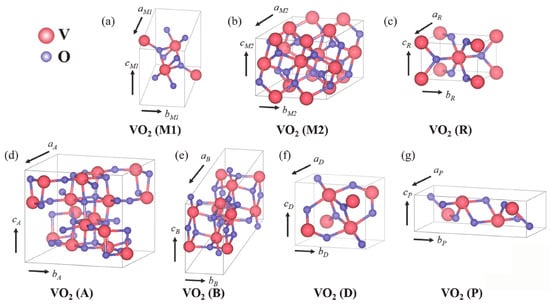
Figure 1.
Crystal structures of VO2 polymorphs (copied from [22]): (a) VO2(M1), (b) VO2(M2), (c) VO2(R), (d) VO2(A), (e) VO2(B), (f) VO2(D), and (g) VO2(P) (reproduced from [22], MDPI open access CC BY 4.0 license, 2021).
VO2(R) is the high-temperature rutile polymorph that exhibits metallic properties and takes part in the IMT [22]. VO2(M) is the most researched low-temperature polymorph that acts as an insulator. The difference between the VO2(M1) and VO2(M2) phases is the arrangement of V atoms along the c-axis. VO2(M2) can be seen as an intermediate phase of the phase transition from VO2(M1) to VO2(R); however, it can be stabilized by introducing doping and high uniaxial pressure [23]. Thus, while both VO2(M1) and VO2(M2) transform into VO2(R) with heating above 67 °C, the VO2(M1) to VO2(R) transition is reversible.
The VO2(A) polymorph can take two crystal structures, low-temperature-phase VO2(AL) and high-temperature-phase VO2(AH), between which a reversible transition exists [24]. Similarly, VO2(M) is also an insulator polymorph exhibiting IMT behavior, and some similar applications have been proposed [25], but the first-order transition to VO2(R) happens at a higher temperature of around 162 °C, making it less attractive for room-temperature applications. VO2(B) is a metastable phase that has a layered structure, making it interesting for applications in supercapacitors and batteries [26]. It is also interesting as a step in the synthesis of VO2(R), to which it transitions through annealing, but at a higher temperature [27].
Another polymorph that can be used to obtain VO2(R), at a lower temperature compared to VO2(B), is VO2(D). It also exhibits magnetic and semiconductive properties [28]. VO2(P) is a conductive polymorph that is considered for applications in batteries [29] and can be transformed to VO2(M) by rapid annealing [22]. Other intermediate phases, including VO2(T), VO2(M3), and VO2(M4), some of which can be stabilized with doping and strain, have been shown in the literature [30,31].
1.2. Physical Characteristics of VO2 Phases
Due to the significant change in properties between the VO2(R) and VO2(M) polymorphs and the reversible, relatively low-temperature transition between the phases, they attract the most interest regarding potential applications. Some of the physical properties of the phases are presented in Table 1, based on [32,33,34].

Table 1.
Some physical properties of VO2(R) and VO2(M).
It is worth noting that while the increase in heat capacity that corresponds to phase change and magnetic susceptibility value change happens at 340 K, the resistivity value change exhibits a hysteresis behavior, where the transition happens at 340 to 325 K when cooling and 335 to 350 K when heating [1,35].
1.3. Possible Mechanisms for the Insulator–Metal Transition
The mechanics of the IMT has been extensively studied, but a comprehensive picture that would explain the underlying mechanisms for the many phenomena observed within VO2 has not been formed yet. The debate primarily revolves around two competing scenarios: Peierls-like or Mott-like transition. Recent theoretical approaches have suggested a potential resolution to the debate, introducing an intermediate perspective known as “Mott-assisted Peierls” or “Mott–Peierls” [36].
A Peierls transition is a phenomenon in which a material undergoes a transition from being a metal to an insulator, caused by a lattice distortion or structural instability in the crystal lattice, with a periodic lattice deformation causing an energy gap [37]. A Mott transition, on the other hand, is triggered by changes in electron density, which can be achievable through pressure or temperature changes when the material is near a critical electron density. The transition arises from the interaction between the Coulomb forces between the electrons and their band width. Due to electron screening, the band width of the electrons is reduced, leading to unbound states that cause the material to behave like a metal at high electron densities [37].
Some studies have supported the VO2 IMT being well described through the Mott-like mechanism. In [38], the Mott transition was supported through the use of infrared spectroscopy. Mott-like transition was also supported through the use of a Raman experiment and an extended Brinkman–Rice picture [39], which extended to Mott transition theory, giving a more detailed explanation of the transition mechanism [40].
Other studies have used the Peierls-like mechanism to describe the behavior of VO2. Using theoretical calculations, VO2 was classified as a Peierls-type insulator in [41], though it was mentioned that there were reasons to consider it a Mott insulator too. An extension of the Peierls approach was used in [42] to calculate the optical properties of VO2, with the calculation agreeing with experimentally measured optical conductivity, along with other studies supporting the Peierls-like mechanism [43,44].
Many studies propose a more nuanced approach that includes both mechanisms in an attempt to more accurately describe the cause of the transition. In [45], it was shown that while the transition in VO2 is caused by both the Mott and Peierls effects, introducing hole doping decouples the states, suggesting further research is needed into the stability of different VO2 phases and the complex interaction between the transition scenarios. Similarly, Ref. [46] explored the influence of doping on VO2, showing either Peierls-like or Mott-like behavior.
The categorization of transitions into “Peierls” or “Mott” was questioned in [47] as an oversimplification. Electrically induced transition and doping experiments have been used to propose that for VO2, the Mott transition should be viewed as a “trigger mechanism” that causes a Peierls-like structural transition. Similar conclusions were reached in [48] and [49], with the authors calling the transition a Mott–Peierls transition. The role of the orbital structure of the vanadium ions in the oxide was discussed in [50] and [51], and the transition was described as a “collaborative” Mott–Peierls transition. The effect of doping on the prevalence of the Mott mechanism in the transition was described through the orbital occupancy of vanadium in [52]. Other studies have also been completed supporting the compound approach [53,54].
So, while a comprehensive picture has not been formed yet, the current research points towards the IMT of VO2 not exclusively being described as a Mott or a Peierls transition, but rather being caused by the lattice deformation in a Peierls-like mechanism that is triggered by a Mott-like change in electron density, which is heavily influenced by doping.
1.4. Publication Trends
As the interest in the material is growing year by year, the purpose of this review is to explore the trends and current state of progress on some of the applications proposed for VO2 in the field of sensors and microactuators.
In the past 20 years, the cumulated number of published papers on the topic has grown to 303 from a search on Scopus and 1322 from Dimensions. To be able to analyze the trend in the number of published papers per year, it was plotted against time, for the last 20 years until 2023, excluding year 2024 as the year is still ongoing (Figure 2). Both the data from Scopus and Dimensions show a rapid growth in interest in the field, especially since around 2008. Similar trends can be seen in the number of citations, as shown in Figure 3. Table 2 presents five of the most cited papers that fall under the searched keywords.
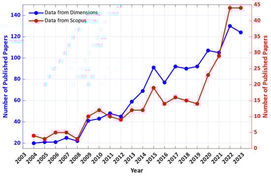
Figure 2.
Number of published papers per year in the last 20 years that relate to vanadium dioxide and microelectronics.
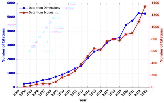
Figure 3.
Number of citations per year in the last 20 years that relate to vanadium dioxide and microelectronics.
Table 2.
Most cited publications on the topic.
1.5. Recent Reviews
Review papers provide a good basis for further research results related to vanadium oxides. The mechanism of its phase change and the physics of its operation are presented in [36,58,59]. Good overviews of the material structure and properties are given in [20,60,61,62,63]. Research on the synthesis of vanadium oxides, deposition methods, fabrication methods, and thin film fabrication are described in [59,60,63,64,65,66,67,68]. The growth of vanadium dioxide nanostructures and nanoparticle synthesis are discussed in [12,22,69]. Improvement in the optical parameters of VO2 is presented in [69].
Articles describing the practical applications of VO2 fall into two categories. Some of the reviews try to cover as many application areas as possible [20,36,59,60,63,66,70,71]. The other type of articles covers one or two application areas in more detail. From [61], we learned about VO2-based electrode design, from [67,69] about coatings, from [72] about applications in photonics, and from [12] about optical sensors. VO2 applications in electronics, optics, and sensors are described in detail in [22]. The research in [68] deals with gas sensors and vapour sensors.
This review paper mainly focuses on recent research results on vanadium dioxide-based actuators and sensors.
2. Applications: Overview
This section presents some key applications of VO2 in the field of sensors and actuators. It focuses on some of the more developed fields of application, which include three sensor types and one microactuator type.
2.1. Resistive Strain Sensor
A resistive strain sensor is a sensor that transforms a mechanical input signal, such as strain, into an electrical signal, in this case, change in resistance. Strain is expressed in a percentage, that is, the difference in length of the sample as a percentage of its length in an unstressed state. Conventionally, a positive strain value corresponds to a sample that is being stretched, i.e., under tensile strain, and a negative value corresponds to compression of the sample.
In [73], VO2 nanobeams were grown using physical vapor deposition on a Si wafer. A nanobeam was transferred to a flexible polystyrene substrate and silver paste was used as electrodes. The device was tested under a strain of −0.25% to 0.25% and showed a relatively linear dependence between resistance and strain, as well as some hysteresis behavior, as shown in Figure 4a. The device is proposed as a sensor to quantify small strain.
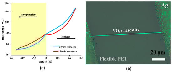
Figure 4.
(a) Device resistance as a function of applied strain, showing hysteresis behavior (reproduced with permission from [73], John Wiley and Sons, 2010), (b) micrograph of a microwire on a flexible substrate strain sensor (reproduced with permission from Ref. [74], Royal Society of Chemistry, 2013).
Chemical vapor deposition was used in [74] to deposit VO2 microwires on a SiO2/Si substrate. Then, the microwire was transferred onto a polyethylene terephthalate (PET) substrate, and silver paint was used as electrodes. The device can be seen in Figure 4b. It was tested under a strain of −0.6% to 0.8%, with the resistance changing relatively linearly as a function of strain. The device is proposed as a flexible strain sensor, in particular, for advanced stress detectors and intelligent bionic devices.
In [75], RF sputtering was used to grow thin films of VO2 on a flexible glass substrate. The device resistance under applied tensile strain changed from around 20 kΩ to around 5 MΩ. The device is proposed for applications in keyboards, pressure-sensitive displays, and touch screens. Polymer-assisted deposition was used in [76] to grow a VO2 thin film on a SiO2/Si substrate, and then, the film was etched into a designed pattern and transferred between polydimethylsiloxane (PDMS) and PET films, attached to Au electrodes. The sensor is a dual-parameter sensor used to monitor a person’s real-time pulse and body temperature. The signals are separated due to different frequency characteristics.
A similar dual-parameter approach was explored in [77], where an ink was manufactured by combining VO2 nanobelt powder with a solution of latex, and deionized water and conductive patterns were drawn onto the substrate using a pen. The flexible sensors were used for speaking, pulse, joint bending, facial expression, hand gesture, and muscle state recognition.
2.2. Resistive Temperature Sensor
A resistive temperature sensor is a sensor that transforms a thermal input signal into an electrical signal, in this case, change in resistance. The temperature coefficient of resistance is defined as the slope of the linear fit for the resistance and temperature dependence. Two dual-parameter resistive temperature sensors presented in [76,77] were covered in the previous sub-section.
Another approach to fabricating a flexible resistive temperature sensor was explored in [78]. It was made by first preparing a poly(styrene–block–butadiene–block–styrene) fabric substrate by electrospinning and pre-treating it with plasma to make it hydrophilic. Then, ink was prepared by mixing vanadium dioxide (VO2) nanoparticles and the aqueous solution of poly(3,4-ethylenedioxythiophene):poly(styrenesulfonate) in deionized water. Then, the VO2 film was spray printed onto the fabric, Ag electrodes were manufactured using an e-beam, and lastly, chemical vapor deposition was used to cover the whole area with an encapsulating layer of parylene.
The sensor was tested in temperatures of 25 °C to 45 °C, where it showed good sensitivity and linearity, as well as a relatively small hysteresis window. While the range of temperatures tested was quite narrow, the sensor is intended for use in soft AI wearables and is mainly meant to measure the temperature of human skin.
A thermal sensor intended for environmental temperature measurements, including applications in agriculture, was developed in [79]. The device was manufactured on a SiO2/Si wafer and consisted of Pt/Ti electrodes and a DC sputtered and annealed thin film of VO2. The sensor was tested under a variety of temperatures from −100 °C to 100 °C and humidities of 10% to 90% relative humidity.
Figure 5 shows the device performance at ambient humidity for the whole range of tested temperatures. The temperature range is divided into three areas, an insulator region (temperatures below IMT), an IMT slope region (62 °C to 68 °C), and a metallic region (temperatures above IMT), with the sensor exhibiting different behaviors in these temperature ranges.
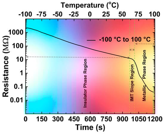
Figure 5.
Device resistance as a function of temperature (reproduced with permission from Ref. [79], American Chemical Society, 2022).
The study also takes into account the influence of humidity on the sensor’s performance. It presents a theoretical explanation for the influence of humidity from a density functional theory standpoint. Figure 6 presents the dependence of the device resistance on relative humidity, from 10% to 90%. In the metallic phase region, Figure 6a, the change in resistance due to the change in humidity seems to be mostly independent from the temperature. However, in the higher temperature region, Figure 6b, the nature of resistance change due to humidity depends on the temperature.
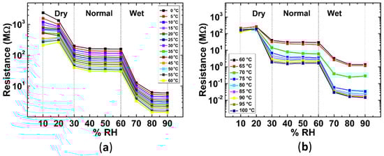
Figure 6.
Device resistance as a function of relative humidity at different temperatures: (a) below transition temperature, (b) above transition temperature (reproduced with permission from Ref. [79], American Chemical Society, 2022).
The humidity range can be divided into dry, normal, and wet conditions, in which the behavior of the sensor is relatively stable with changes in humidity. Overall, with increasing humidity, the resistance decreased, while keeping the overall temperature dependence. The sensor can be used for temperature sensing under any humidity conditions with some digital processing of the signal or additional packaging.
2.3. Mechanical Microactuators
A mechanical microactuator is an actuator that transforms an electrical input signal of some power, measured in Watts, to a mechanical output signal, expressed as deformation or displacement, as measured in the percentage of a respective size or µm, respectively.
One study [80] proposes a vertical stack cantilever microactuator structure. To fabricate it, first, physical vapor deposition was used to deposit Si3N4 on a Si substrate. Then, ITO was deposited as the bottom electrode via e-beam evaporation. A layer of VO2 was sputtered on top via RF magnetron sputtering and patterned using reactive ion etching. The top Pt electrode was deposited on top using e-beam evaporation. Then, the ITO and Si3N4 layers were reactive iron etched to open channels for substrate release through XeF2 etching.
Actuator deformation occurs at the phase transition of VO2, caused by global heating or electrically induced heating. The observed tip displacement for a cantilever length of 35 µm was 2 µm under global heating and 0.22 µm under electrically induced heating. This order of magnitude difference can be explained due to the uneven heating of the structure under electrically induced heating.
The study also reported electrical measurements, including the structure’s total resistance change due to applied voltage, observing a significant hysteresis effect, where the phase transition was observed at 1.95 V when increasing the voltage and 1.05 V when decreasing it. The study authors also proposed an electrical resistance model of the cantilever and performed a finite element modelling (FEM) simulation, which predicted a greater tip displacement. The difference was possibly attributed to the heat-induced stress being partially released through defects and grain boundaries in the VO2 layer as opposed to producing strain.
Another stacked cantilever structure was explored in [81]. To fabricate the actuator, a layer of SiO2 was deposited by plasma-enhanced chemical vapor deposition on a Si substrate. Then, an adhesion layer of Ti and Pt electrodes were deposited by evaporation and patterned by lift-off. A sacrificial layer of Si was deposited on top via low-pressure chemical vapor deposition and patterned by reactive ion etching. Then, a SiO2 layer was deposited on top via low-pressure chemical vapor deposition and patterned using plasma etching. The second Ti/Pt metal layer forming an integrated resistive heater was sputtered and pattered via lift-off. Then, a layer of SiO2 was deposited on top and the structures were released using XeF2 after dicing. Finally, a VO2 thin film was deposited with pulsed laser deposition using a shadow mask.
The displacement versus actuation current characteristic was studied in two environments: in air and in a vacuum. The electrical power required to achieve full actuation was reported to be 16 times greater in air than in the vacuum. The tip displacement was not 0 at 0 current applied because it was measured from a flat state and there was some residual deformation caused by the fabrication process. FEM simulation was used to simulate the tip displacement.
Another approach to VO2 microactuators is proposed in [82]. The actuator was manufactured by first depositing VO2 on a SiO2/Si substrate using pulsed laser deposition. Then, a Cr layer was deposited with e-beam evaporation and lithographically patterned. Then a photoresistant pattern was defined to protect the fixed ends of future cantilevers, and the exposed VO2 was reactive ion etched and finally released by buffered oxide etching. At room temperature, the released structures curved towards the Cr layer and the curvature decreased with the phase transition of VO2, as shown in Figure 7a.
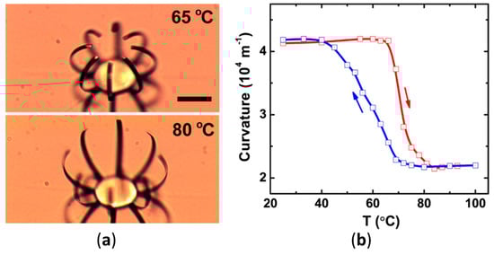
Figure 7.
(a) Device shape before the phase transition (top, at 65 °C) and after (bottom, 80 °C), (b) curvature of the actuator as a function of its temperature (reproduced with permission from Ref. [82], American Chemical Society, 2012).
Two actuation methods were proposed for the actuator: electrical or light actuation. The tip displacement observed was 36 µm for a 60 µm long structure. In the study, both displacement and curvature values were considered, due to curvature being a more intuitive measurement for this type of actuator. Figure 7b shows the curvature dependence from temperature.
When the device was actuated via laser, the required power was around 4 mW. Depending on where the laser was focused, either the whole palm or individual fingers could be actuated. When the device was actuated electrically, a 1.4 V voltage was applied, with 1.6 mW of electrical power causing maximum displacement.
Direct laser writing was used in [83] to produce a microactuator. To achieve this, a VO2 film was laser patterned, then the achieved microbelt structure was detached from the film using a tungsten probe and transferred to a SiO2 substrate. It was fixed using silver paste on one end and coated with a Cr layer. FEM simulation was used to determine the optimal thickness of the Cr layer.
To activate the actuator, the authors used two approaches: light and electrical. To use light for actuation, a laser with a wavelength of 808 nm was used to cause the VO2 heating, with a 250 mW laser causing a 25 µm tip displacement for a 40 µm cantilever. By attaching the microcantilever to a microchip with Au electrodes, the actuator could be activated with electrical current, resulting in 30 µm deflection at 120 mW electrical power applied, and the cantilever deformation can be seen in Figure 8a.
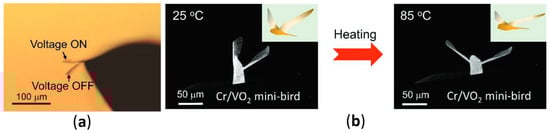
Figure 8.
(a) Microbelt device in deformed and undeformed states, (b) bird-shaped microactuator (reproduced with permission from [83]. John Wiley and Sons, 2022).
To show the possibilities of direct laser writing for microactuator fabrication, a bird-shaped actuator was manufactured, as shown in Figure 8b. The actuator was actuated by temperature via a heating stage, changing the temperature from 25 °C to 85 °C.
A more sophisticated approach to actuator control was used in [84] by incorporating a self-sensing electrode into the structure and employing a PID controller. The device was fabricated by first depositing a layer of SiO2 on a Si wafer using low-temperature oxide. Then, a layer of Ti and Pt were deposited using thermal evaporation and patterned with lift-off. A second SiO2 layer was deposited on top and patterned using deep reactive ion etching. Then, the cantilever was released using XeF2, and finally, a layer of VO2 was deposited using pulsed laser deposition.
Electrical current up to 5 mA was applied to achieve deflection of up to 100 µm for a cantilever of 550 µm in length. The resistance of the device was measured using the self-sensing electrodes, and a Boltzmann function was used to approximate the actual deflection from the resistance measurement; this approximation was then used as a feedback signal for a PID controller to adjust the driving current.
3. Comprehensive Review
This section presents a comprehensive review of the proposed applications for VO2 in the field of sensors and actuators, which inherently led to some applications being excluded due to their limited relation to the field of focus of the review. Some of the notable applications that were excluded from the review include the following:
- thermochromic films for smart window applications [85];
- thermal camouflage [86];
- radiators [87];
- applications as electrodes for batteries [88];
- applications as electrodes for supercapacitors [89];
- optical temperature sensors [90,91];
- electrical switches [92,93];
- field–effect transistors [94];
- photoinduced mechanical actuators [95];
- optical and thermal memory devices [96].
The key features used to compare the studies were the nature of input, nature of output, fabrication method, and technology readiness level. The nature of input and output describe the physical domains involved in the device operation. For sensors, the input is the sensed quantity and the output is the measured quantity. For actuators and switches, the input is the control quantity and the output quantity is the actuated or controlled quantity.
Where the data were available, the input column also includes information about the specific quantity and the range studied in the paper, and the output column includes the specific quantity and either the sensitivity achieved or the range corresponding to the range of input. In some cases, the output was measured indirectly (for example, resistivity change measured using voltage), so the column includes both the quantity changing and the quantity measured.
The fabrication methods column briefly mentions the methods used to fabricate the VO2 structures and the type of structure fabricated for the particular device. Another key feature that was compared between the studies was the technology readiness level (TRL). The idea behind it is to show where a technology is in terms of development, with the lowest score corresponding to basic principles being observed and a theoretical application proposed, and the highest score corresponding to the technology being used commercially. While the assessment was inherently somewhat subjective, the scale used was loosely based on [97].
A score of 1 was given to applications that were proposed on the basis of a measurement of a physical property change in VO2. If a study also included more in-depth theoretical work related to the application, for example a simulation, a score of 2 was given. If the study included a fabricated device, the score was 3, and if it went beyond basic characterization of the device, for example, testing it in a specific application or a variety of different conditions, the score went up to 4. The highest score given in the comparison was 5, which went to the studies that demonstrated more robust prototypes with some level of reliability considerations.
The applications considered in Table 3 include applications for sensors and actuators. The sensors are mostly resistive, with a few examples of piezoelectric sensors. Also, mechanical actuators with electrical or optical inputs are being developed.
Table 3.
Review of recent papers concerning VO2 applications in the sensor and actuator fields.
4. Discussion
Different applications of VO2 were considered in this review, with a focus on applications in sensors and actuators. Most of the sensors seem to be resistive in nature, relying on the resistivity change in VO2 under different changes in conditions; however, piezoelectric sensors have also been proposed. The most developed sensors that were looked at were resistive temperature sensors and resistive strain sensors. The idea of a mechanical microactuator is also being developed, as shown in multiple studies.
4.1. Applications: Further Discussion
The applications considered in this review include electrical, optical, thermal, mechanical, fluidic, and chemical domains. Also, some of the studies covered in this review have proposed dual-parameter sensors, which combine two sensors in one structure, such as a combined temperature and strain sensor.
4.1.1. Resistive Strain Sensors
Different approaches to manufacturing a strain sensor using VO2 are being developed, with some of the studies showing a higher technology readiness level, where the manufactured prototypes are tested for repeatability and reliability, as well as applied to concrete applications, such as human health monitoring. Some of the devices are intended to be used as push switches, some as strain sensors, and others as combined temperature and strain sensors.
The information from the studies that provided enough data to conclude the sensitivity characteristics of the sensors was compiled into the Figure 9, which shows the dependence between the resistance ratio (the resistance at a given strain divided by the resistance at no strain) and strain (the length of the sample divided by the length of the unstressed sample), both expressed in percentages.
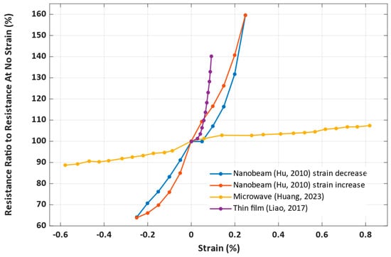
Figure 9.
Sensitivity and measurement ranges of proposed strain sensors, based on (Hu, 2010) [73], (Huang, 2023) [74], and (Liao, 2017) [76].
The microwire sensor in [74] was tested for the highest bidirectional strain, −0.6% to 0.8%. Compared to other presented sensors, it has a good linearity, but a lower sensitivity. The thin film sensor in [75] has a higher sensitivity, but a poor linearity. The nanobeam sensor in [73] presents a sensor with both a good linearity and higher sensitivity, tested for strains −0.25% to 0.25%. The ink sensor in [77] was tested for strains from 0% to 3%, but the paper did not directly present data on the device’s sensitivity.
4.1.2. Resistive Temperature Sensors
Temperature sensors have been developed using different manufacturing approaches, with the most used structures being films and powders. These applications show the greatest technology readiness levels among the applications considered. Some of the considered sensors are dual-parameter sensors, combining strain and temperature sensing into one device. Such devices are proposed especially for human monitoring and AI wearable applications, such as using a temperature sensor to access human body temperature and strain sensing to access pulse, facial expressions, hand gestures, etc.
The two more technologically ready sensors, [77,78], are produced by forming an ink as opposed to thin film deposition, with this fabrication approach being easier in the lab, making development quicker, but not necessarily ensuring further quick development as the technology moves towards scaling.
Due to VO2 showing different properties before, during, and after phase transition, the operating range of a sensor can be defined to operate in one of the regions with a more linear characteristic or across multiple regions with a more complex characteristic. Figure 10 shows a summary of the proposed thermal sensors, their sensitivities, expressed as temperature coefficients of resistance, and their operating ranges. It is important to note that the temperature coefficients shown in Figure 10 somewhat differ from the values mentioned in the corresponding studies, as the coefficients were calculated for each of the points separately in order to show the temperature coefficient dependency on the operating temperature as opposed to obtaining an average value by calculating it from a linear fit of the data.
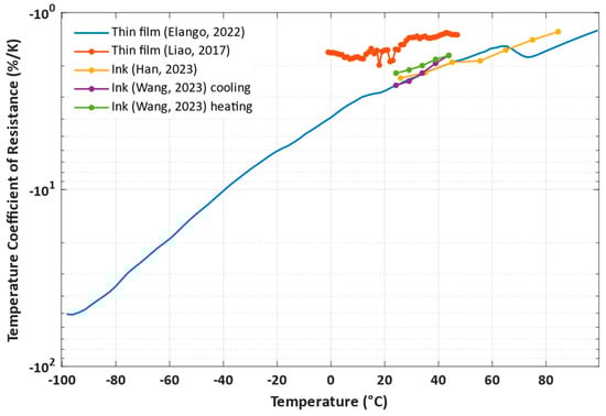
Figure 10.
Sensitivity and measurement ranges of proposed temperature sensors, based on (Liao, 2017) [76], (Han, 2023) [77], (Wang, 2023) [78], and (Elango, 2022) [79].
The considered temperature sensors operate in different temperature ranges, with many of the studies focusing on ranges appropriate for environmental and human-related temperature measurements. The best combination of linearity and high sensitivity is shown by [78], which operates in a narrow range of 25 °C to 45 °C. The greatest temperature range studied was −100 °C to 100 °C in [79], which also employed density functional theory computational studies and experimental measurements to determine the device’s performance under different humidity conditions. The study found that while there was a resistance change and temperature response rate change caused by humidity, by classifying the humidity conditions as dry, normal, and wet, the behaviour of the sensor could be relatively easily described in each of the regions.
4.1.3. Resistive Gas Concentration Sensors
Resistive gas concentration sensors are being developed based on VO2 nanostructures (nanosheets and nanorods) and composite structures, which include materials such as Pd, WO3, Ag, and MoTe2. Experimental samples are being developed to detect different gases, such as NO2 in concentrations from 0.5 to 5 ppm, H2 in concentrations from 1 to 1000 ppm, and CH4 in concentrations from 500 to 4500 ppm [103,104,105,106,107].
4.1.4. Mechanical Microactuators
Most of the microactuators considered in this review are microcantilever structures, with some kind of thin film stacking. Some of the works are based on VO2/Cr stacks, while others combine three to five layers. The most used method to deposit VO2 films was pulsed laser deposition. RF sputtering was also used. To pattern the films, most commonly, etching, and in one study, femtosecond laser direct writing were used. The proposed actuators switch between their undeformed and deformed states. While some works proposing continuous actuation as opposed to switching were found, it does not seem to be a viable approach without employing a feedback control system.
Many of the covered studies include multiple types of actuation, namely, directly thermal, optical with heating via laser, and electrical. For the purposes of this review, electrical actuation was considered. The electrical power applied to structures to ensure the switches was up to an order of magnitude different between the considered studies. Some studies, such as [83], showed similar deformations regardless of the actuation type. However, in others, for example in [80], the displacement due to electrical heating was almost ten times smaller than the displacement due to global heating. This hints to uniform power and heat distribution being a challenge for the electrical actuation of such actuators. However, many of the proposed designs tackled this challenge quite well.
The sizes of the deforming parts of devices varied between the proposed solutions, with the smallest one being 35 µm long and the longest one being 550 µm. The output variable, mechanical displacement, was expressed as a percentage of the device length to allow for a comparison of the differently sized devices more fairly. However, care should be taken to not extrapolate the measured displacement/length ratio to different lengths, as the studies that compared multiple similar structures of different sizes showed different displacement/length ratios. The information about the sizes and displacements of the considered structures were compiled as Figure 11.
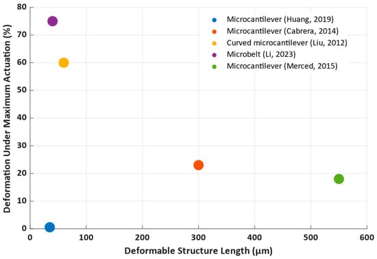
Figure 11.
Relative deformation of the proposed microactuators and their sizes, based on (Huang, 2019) [80], (Cabrera, 2014) [81], (Liu, 2012) [82], (Li, 2023) [83], and (Merced, 2015) [84].
The smallest deformation among the considered studies was shown by [80], due to issues with uneven heating of the VO2 structure under electrically induced heating. Two longer devices showed a moderate displacement of 23% [81] and 18% [84]. Good performance was achieved in [84] by integrating a resistance sensor into the structure itself, which allowed for self-sensing of the actual actuator deformation and using a PID controller to more precisely control the actuator deflection. The highest deformation of 75% [83] and 60% [82] corresponded to the smaller devices. In both studies, the devices had a bent shape with a relatively high curvature and flattened, fully or partially, when voltage was applied.
Environmental conditions were also considered in some of the studies, with all actuators being tested in air, but some additionally in water and in a vacuum. Significant differences in actuation energy were observed for different environments, which is attributed mainly to different rates of heat exchange between the VO2 actuating layer and the environment.
4.1.5. Other Applications
Other applications considered in this review are a resistive photodetector [98,99,100,101], piezoelectric strain sensor [102], and thermal fluid flow sensor [108,109]. While the piezoelectric effect was observed in VO2, the application as a strain sensor is only theoretically proposed. The application as a fluid sensor for microfluidics explores the thermally induced change in the resistivity of VO2 as applied to fluid flow measurement, with some sample devices being manufactured.
4.2. Performance Modification Methods
The methods of tuning the VO2 properties and phase change temperature observed in the reviewed studies include doping, using various nanostructures, such as microbelts, microwires, nanocrystals, nanosheets, etc., and synthesizing different types of composite structures, including thin film stacks and different combinations of nanoparticles.
4.3. Fabrication Methods and Structures
There does not seem to be a strong correlation between the type of sensor developed and the structure used, and different structures are being explored for different applications. Thin film structures are very popular for both actuators and different types of sensors. The methods for fabricating thin films are mostly different physical vapor deposition approaches, most notably pulsed laser deposition, DC sputtering, and RF sputtering.
Some applications use VO2 in ink formed by using a VO2 powder suspended in a liquid (example applications include photodetector, temperature, and strain sensors) [77,78,99]. This approach simplifies the manufacture of VO2 devices, at least at a laboratory test scale, and does not necessarily seem to yield devices with worse sensitivity values than other methods. Similarly, some gas sensors use drop and spin coating with a VO2 powder [104] or a nanorod solution [105].
Other structures explored include microbelts [83], microwires [74], micro- and nanocrystals [102], and single crystal nanobeams [73], for which both chemical and physical deposition methods are used. A microbelt structure, used as a mechanical microactuator, does not seem to lead to a superior sensitivity compared to thin film structures, as well as microwires, used in a resistive strain sensor application. Micro- and nanocrystals have been used as piezoelectric strain sensors, but the application of VO2 as a piezoelectric material does not seem to have been as actively explored as its application in resistive-type sensors and is in a rather theoretical state now. Single crystal nanobeams have been proposed for strain sensor applications and seem to provide a better sensitivity as compared to thin film counterparts.
Also, it has to be noted that the structures used in the studies with the highest technology readiness level were thin films, produced using DC sputtering [79,98], pulsed laser deposition [82], and polymer-assisted deposition [76], as well as ink-based designs [77,78].
5. Key Challenges
While VO2 is an exciting material with possible applications in many fields of technology, there are challenges related to its use in different applications.
5.1. Opportunities to Apply VO2 in Different Domains
The dependence between the temperature and resistivity of VO2 is one of the possible properties of the material that can be targeted to develop new devices; however, there are many other possible domains that can be affected by the change in properties or in which the phase transition can be triggered. This leaves an open opportunity to explore more ways to apply VO2 in different devices and fields.
5.2. Performance-Related Challenges
A lot of applications of VO2 rely specifically on the IMT region. However, the temperature at which it happens, while reasonably close to room temperature, is still not practical for many applications and has to be modified using different approaches, which can for example, greatly increase hysteresis [22]. Furthermore, some applications rely on switching performance and some sensors require a linear characteristic change, further expanding the performance modification scope.
5.3. Manufacturing Challenges
There are different methods of manufacturing single-crystal and polycrystalline films and nanostructures. However, it is still challenging to precisely controlling the manufacture of VO2 nanostructures and achieving a high quality of films [36]. Currently, there is no simple, highly productive, and CMOS-compatible manufacturing approach for VO2 structures [71], and different approaches are being explored for manufacturing VO2-based devices.
5.4. Solutions
Recent studies have shown that an intermediate metallic phase is also formed in VO2 thin films during the insulator–metal transformation due to the presence of donor impurities [110]. In addition, further metastable phases are also formed. The simultaneous presence of different phases can cause mechanical fatigue and malfunction in VO2-based micro- and nano-scale devices [70]. Further research is needed to address this problem.
To increase the commercialization of VO2 devices, it would be necessary to develop low-cost and high-volume manufacturing methods for VO2(M)-phase micro-/nanowires and nanostructures free of unwanted phases [65].
The size of the nanowire has a direct impact on the behavior of the VO2 IMT. Being able to precisely control the size and alignment of VO2 structures is a problem that needs solving [22].
In electronic devices, the IMT temperature of ~68 °C is often too high. This is currently reduced by the addition of dopants to the VO2, but the consequence is a slow transition rate and large hysteresis window [22]. There is a need to develop a method to reduce the IMT temperature without deteriorating these parameters. Furthermore, macroscopic defects (voids) cause local stresses and thus significantly affect the device performance. A possible solution exists by using a focused ion beam (FIB) and nanoindentation, such that the shape, location, and volume of macroscopic defects can be precisely controlled, allowing the hysteresis loop, IMT temperature, and conductivity to be tuned.
For VO2 in direct contact with air, device degradation may be caused by oxidation of V4+ ions to V5+ [70]. To solve this, the use of a passivation layer, encapsulation, and a VO2 core–shell structure can ensure better-quality VO2 films.
The hydrophobic HfO2 encapsulation structure can be used to prolong the lifetime of VO2 films, which also have excellent optical properties [111].
It is necessary to increase the stability of vanadium oxide devices against thermal, light, moisture, and oxygen environmental factors [20]. This requires a deeper understanding of their degradation mechanisms.
Vanadium oxides are toxic and can damage the liver, bones, and DNA of leukocytes, among other things [20]. Environmental impacts can be reduced by designing the manufacturing process and waste management appropriately. The encapsulation of the devices and application of silica coatings can seal vanadium from air and water.
The application of vanadium dioxide in IC devices is often limited by its thermal stability. VOx phase transition occurs at relatively low temperatures, which can be a significant bottleneck.
One of the methods that is used to modulate the critical temperature in vanadium dioxide was presented in [60], where it was shown how critical temperature could be adjusted through chemical doping, stoichiometric engineering, and advanced fabrication techniques.
Another vital approach is device structure optimization; the structure of the device using VOx should be optimized to reduce the thermal load on the material and improve the thermal dissipation characteristics of the device. At the system level, thermal management in the overall IC system is also crucial. This includes designing ICs with efficient heat dissipation paths, using materials with good thermal conductivity as heat spreaders, and managing the power consumption patterns of the ICs to minimize localized heating.
6. Conclusions
This paper highlights the evolving research on VO2, delving into its properties, phase transition mechanics, and potential applications. Studies on VO2, especially in the context of its insulator–metal transition and its resistivity change, have been ongoing since the 1960s. However, its relevance in the sensor and actuator field has surged in recent years, as evidenced by a significant increase in related publications and citations since 2010. According to the Dimensions database and Scopus, the annual output of VO2-focused studies in sensors and actuators has reached over 140 and 40, respectively, with citations exceeding 12,000 and 1000 in each database.
This review primarily focused on VO2’s applications in sensors and actuators. Most sensors based on VO2 are resistive, building on its change in resistivity under varying conditions. However, piezoelectric sensors are also emerging. The most advanced of these are resistive temperature and strain sensors. Additionally, the development of mechanical microactuators using VO2 is gaining more attention.
Despite these advancements, there is a need for further research to develop simpler, more robust, and reliable VO2-based sensors and actuators. The sustained interest in VO2 for various applications is evident, with ongoing research exploring both new uses and enhancements to existing designs. The scope of this research spans from theoretical materials science studies for a deeper understanding of VO2 to practical aspects such as simplifying device fabrication for mass production.
Author Contributions
Conceptualization, L.P.; methodology, Y.Z.; formal analysis, Y.Z.; investigation, Y.Z.; resources, Y.Z.; data curation, Y.Z. and M.D.; writing—original draft preparation, Y.Z.; writing—review and editing, M.D.; visualization, Y.Z. and M.D.; supervision, L.P. All authors have read and agreed to the published version of the manuscript.
Funding
This research received no external funding.
Data Availability Statement
The data presented in this study are available upon request from the corresponding author.
Conflicts of Interest
The authors declare no conflicts of interest.
References
- Morin, F.J. Oxides Which Show a Metal-to-Insulator Transition at the Neel Temperature. Phys. Rev. Lett. 1959, 3, 34–36. [Google Scholar] [CrossRef]
- Huang, Y.; Zhang, D.; Liu, Y.; Jin, J.; Yang, Y.; Chen, T.; Guan, H.; Fan, P.; Lv, W. Phase Transition Analysis of Thermochromic VO2 Thin Films by Temperature-Dependent Raman Scattering and Ellipsometry. Appl. Surf. Sci. 2018, 456, 545–551. [Google Scholar] [CrossRef]
- Nag, J.; Haglund, R.F.; Andrew Payzant, E.; More, K.L. Non-Congruence of Thermally Driven Structural and Electronic Transitions in VO2. J. Appl. Phys. 2012, 112, 103532. [Google Scholar] [CrossRef]
- Yu, Z.; Liu, Y.; Zhang, Z.; Cheng, M.; Zou, Z.; Lu, Z.; Wang, D.; Shi, J.; Xiong, R. Controllable Phase Transition Temperature by Regulating Interfacial Strain of Epitaxial VO2 Films. Ceram. Int. 2020, 46, 12393–12399. [Google Scholar] [CrossRef]
- Cao, J.; Ertekin, E.; Srinivasan, V.; Fan, W.; Huang, S.; Zheng, H.; Yim, J.W.L.; Khanal, D.R.; Ogletree, D.F.; Grossman, J.C.; et al. Strain Engineering and One-Dimensional Organization of Metal–Insulator Domains in Single-Crystal Vanadium Dioxide Beams. Nat. Nanotechnol. 2009, 4, 732–737. [Google Scholar] [CrossRef]
- Chen, Y.; Zhang, S.; Ke, F.; Ko, C.; Lee, S.; Liu, K.; Chen, B.; Ager, J.W.; Jeanloz, R.; Eyert, V.; et al. Pressure–Temperature Phase Diagram of Vanadium Dioxide. Nano Lett. 2017, 17, 2512–2516. [Google Scholar] [CrossRef]
- Li, Q.; Zhang, H.; Lin, C.; Tian, F.; Smith, J.S.; Park, C.; Liu, B.; Shen, G. Pressure-Induced Phase Transitions and Insulator-Metal Transitions in VO2 Nanoparticles. J. Alloys. Compd. 2017, 709, 260–266. [Google Scholar] [CrossRef]
- Wegkamp, D.; Herzog, M.; Xian, L.; Gatti, M.; Cudazzo, P.; McGahan, C.L.; Marvel, R.E.; Haglund, R.F.; Rubio, A.; Wolf, M.; et al. Instantaneous Band Gap Collapse in Photoexcited Monoclinic VO2 Due to Photocarrier Doping. Phys. Rev. Lett. 2014, 113, 216401. [Google Scholar] [CrossRef]
- Becker, M.F.; Buckman, A.B.; Walser, R.M.; Lépine, T.; Georges, P.; Brun, A. Femtosecond Laser Excitation of the Semiconductor-metal Phase Transition in VO2. Appl. Phys. Lett. 1994, 65, 1507–1509. [Google Scholar] [CrossRef]
- Schwartz, M. (Ed.) Encyclopedia of Smart Materials, 1st ed.; Wiley: Hoboken, NJ, USA, 2002; ISBN 978-0-471-17780-7. [Google Scholar]
- Birkhölzer, Y.A.; Sotthewes, K.; Gauquelin, N.; Riekehr, L.; Jannis, D.; Van Der Minne, E.; Bu, Y.; Verbeeck, J.; Zandvliet, H.J.W.; Koster, G.; et al. High-Strain-Induced Local Modification of the Electronic Properties of VO2 Thin Films. ACS Appl. Electron. Mater. 2022, 4, 6020–6028. [Google Scholar] [CrossRef] [PubMed]
- Yoon, J.; Hong, W.-K.; Kim, Y.; Park, S.-Y. Nanostructured Vanadium Dioxide Materials for Optical Sensing Applications. Sensors 2023, 23, 6715. [Google Scholar] [CrossRef] [PubMed]
- Guo, P.; Biegler, Z.; Back, T.; Sarangan, A. Vanadium Dioxide Phase Change Thin Films Produced by Thermal Oxidation of Metallic Vanadium. Thin Solid. Films 2020, 707, 138117. [Google Scholar] [CrossRef]
- Darwish, M.; Neumann, P.; Mizsei, J.; Pohl, L. Electro-Thermal Simulation of Vertical VO2 Thermal-Electronic Circuit Elements. Energies 2020, 13, 3447. [Google Scholar] [CrossRef]
- Pohl, L.; Darwish, M.; Mizsei, J. Electro-Thermal Investigation of SMT Resistors for Thermal-Electrical Logic Circuits by Simulation. In Proceedings of the 2019 25th International Workshop on Thermal Investigations of ICs and Systems (THERMINIC), Lecco, Italy, 25–27 September 2019; IEEE: Piscataway, NJ, USA, 2019; pp. 1–4. [Google Scholar]
- Del Valle, J.; Rocco, R.; Domínguez, C.; Fowlie, J.; Gariglio, S.; Rozenberg, M.J.; Triscone, J.-M. Dynamics of the Electrically Induced Insulator-to-Metal Transition in Rare-Earth Nickelates. Phys. Rev. B 2021, 104, 165141. [Google Scholar] [CrossRef]
- Wegkamp, D.; Stähler, J. Ultrafast Dynamics during the Photoinduced Phase Transition in VO2. Prog. Surf. Sci. 2015, 90, 464–502. [Google Scholar] [CrossRef]
- Srivastava, A.; Rotella, H.; Saha, S.; Pal, B.; Kalon, G.; Mathew, S.; Motapothula, M.; Dykas, M.; Yang, P.; Okunishi, E.; et al. Selective Growth of Single Phase VO2(A, B, and M) Polymorph thin Films. APL Mater. 2015, 3, 026101. [Google Scholar] [CrossRef]
- Kumi-Barimah, E.; Anagnostou, D.E.; Jose, G. Phase Changeable Vanadium Dioxide (VO2) thin Films Grown from Vanadium Pentoxide (V2O2) using Femtosecond Pulsed Laser Deposition. AIP Adv. 2020, 10, 065225. [Google Scholar] [CrossRef]
- Hu, P.; Hu, P.; Vu, T.D.; Li, M.; Wang, S.; Ke, Y.; Zeng, X.; Mai, L.; Long, Y. Vanadium Oxide: Phase Diagrams, Structures, Synthesis, and Applications. Chem. Rev. 2023, 123, 4353–4415. [Google Scholar] [CrossRef]
- Eyert, V. The metal-insulator transitions of VO2: A band theoretical approach. Ann. Phys. 2002, 514, 650–704. [Google Scholar] [CrossRef]
- Zhang, Y.; Xiong, W.; Chen, W.; Zheng, Y. Recent Progress on Vanadium Dioxide Nanostructures and Devices: Fabrication, Properties, Applications and Perspectives. Nanomaterials 2021, 11, 338. [Google Scholar] [CrossRef] [PubMed]
- Sohn, J.I.; Joo, H.J.; Ahn, D.; Lee, H.H.; Porter, A.E.; Kim, K.; Kang, D.J.; Welland, M.E. Surface-Stress-Induced Mott Transition and Nature of Associated Spatial Phase Transition in Single Crystalline VO2 Nanowires. Nano Lett. 2009, 9, 3392–3397. [Google Scholar] [CrossRef] [PubMed]
- Oka, Y.; Sato, S.; Yao, T.; Yamamoto, N. Crystal Structures and Transition Mechanism of VO2(A). J. Solid. State Chem. 1998, 141, 594–598. [Google Scholar] [CrossRef]
- Zhang, Y. VO2(B) conversion to VO2(A) and VO2(M) and their oxidation resistance and optical switching properties. Mater. Sci. Pol. 2016, 34, 169–176. [Google Scholar] [CrossRef]
- Zhang, Y.; Huang, Y. A facile hydrothermal synthesis of tungsten doped monoclinic vanadium dioxide with B phase for supercapacitor electrode with pseudocapacitance. Mater. Lett. 2016, 182, 285–288. [Google Scholar] [CrossRef]
- Popuri, S.R.; Miclau, M.; Artemenko, A.; Labrugere, C.; Villesuzanne, A.; Pollet, M. Rapid Hydrothermal Synthesis of VO2(B) and Its Conversion to Thermochromic VO2(M1). Inorg. Chem. 2013, 52, 4780–4785. [Google Scholar] [CrossRef] [PubMed]
- Liu, L.; Cao, F.; Yao, T.; Xu, Y.; Zhou, M.; Qu, B.; Pan, B.; Wu, C.; Wei, S.; Xie, Y. New-phase VO2 Micro/Nanostructures: Investigation of Phase Transformation and Magnetic Property. New J. Chem. 2012, 36, 619–625. [Google Scholar] [CrossRef]
- Wang, Z.; Yu, K.; Feng, Y.; Qi, R.; Ren, J.; Zhu, Z. VO2(p)-V2C(MXene) Grid Structure as a Lithium Polysulfide Catalytic Host for High-Performance Li–S Battery. ACS Appl. Mater. Interfaces 2019, 11, 44282–44292. [Google Scholar] [CrossRef]
- Pouget, J.P.; Launois, H.; Rice, T.M.; Dernier, P.; Gossard, A.; Villeneuve, G.; Hagenmuller, P. Dimerization of a linear Heisenberg Chain in the Insulating Phases of V1-xCrxO2. Phys. Rev. B 1974, 10, 1801–1815. [Google Scholar] [CrossRef]
- Villeneuve, G.; Drillon, M.; Hagenmuller, P. Contribution a l’etude structurale des phases V1−xCrxO2. Mater. Res. Bull. 1973, 8, 1111–1121. [Google Scholar] [CrossRef]
- Berglund, C.N.; Guggenheim, H.J. Electronic Properties of VO2 near the Semiconductor-Metal Transition. Phys. Rev. 1969, 185, 1022–1033. [Google Scholar] [CrossRef]
- Guan, S.; Rougier, A.; Suchomel, M.R.; Penin, N.; Bodiang, K.; Gaudon, M. Geometric Considerations of the Monoclinic–Rutile Structural Transition in VO2. Dalton Trans. 2019, 48, 9260–9265. [Google Scholar] [CrossRef] [PubMed]
- Wang, C.; Zhao, L.; Liang, Z.; Dong, B.; Wan, L.; Wang, S. New intelligent multifunctional SiO2/VO2 Composite Films with Enhanced Infrared Light Regulation Performance, Solar Modulation Capability, and Superhydrophobicity. Sci. Technol. Adv. Mater. 2017, 18, 563–573. [Google Scholar] [CrossRef]
- Morin, F.J. Halides, Oxides, and Sulfides of the Transition Metals. J. Appl. Phys. 1961, 32, 2195–2197. [Google Scholar] [CrossRef]
- Liu, K.; Lee, S.; Yang, S.; Delaire, O.; Wu, J. Recent progresses on physics and applications of vanadium dioxide. Mater. Today 2018, 21, 875–896. [Google Scholar] [CrossRef]
- Kittel, C. Introduction to Solid State Physics, 9th ed.; Global Edition; Wiley: Hoboken, NJ, USA, 2018; ISBN 978-1-119-45416-8. [Google Scholar]
- Qazilbash, M.M.; Brehm, M.; Chae, B.-G.; Ho, P.-C.; Andreev, G.O.; Kim, B.-J.; Yun, S.J.; Balatsky, A.V.; Maple, M.B.; Keilmann, F.; et al. Mott Transition in VO2 Revealed by Infrared Spectroscopy and Nano-Imaging. Science 2007, 318, 1750–1753. [Google Scholar] [CrossRef] [PubMed]
- Kim, H.-T. Extension of the Brinkman-Rice Picture and the Mott Transition. Phys. C Supercond. 2000, 341–348, 259–260. [Google Scholar] [CrossRef]
- Kim, H.-T.; Chae, B.-G.; Youn, D.-H.; Maeng, S.-L.; Kim, G.; Kang, K.-Y.; Lim, Y.-S. Mechanism and Observation of Mott Transition in VO2–Based Two- and Three-Terminal Devices. New J. Phys. 2004, 6, 52. [Google Scholar] [CrossRef]
- Wentzcovitch, R.M.; Schulz, W.W.; Allen, P.B. VO2: Peierls or Mott-Hubbard? A view from band theory. Phys. Rev. Lett. 1994, 72, 3389–3392. [Google Scholar] [CrossRef] [PubMed]
- Tomczak, J.M.; Biermann, S. Optical Properties of Correlated Materials: Generalized Peierls Approach and Its Application to VO2. Phys. Rev. B 2009, 80, 085117. [Google Scholar] [CrossRef]
- Goodenough, J.B. The Two Components of the Crystallographic Transition in VO2. J. Solid. State Chem. 1971, 3, 490–500. [Google Scholar] [CrossRef]
- Semenov, A.L. Dynamics of a Peierls System in a Light Field. J. Exp. Theor. Phys. 1999, 89, 1168–1179. [Google Scholar] [CrossRef]
- Ling, C.; Wang, Q.; Wang, X.; Zhao, Z.; Wang, Z.; Li, J.; Zhao, Y.; Jin, H. Hole Dopants Disentangling Peierls–Mott Relevance States of VO2 by First-Principles Calculation. J. Phys. Chem. C 2021, 125, 5816–5823. [Google Scholar] [CrossRef]
- Sakai, E.; Yoshimatsu, K.; Shibuya, K.; Kumigashira, H.; Ikenaga, E.; Kawasaki, M.; Tokura, Y.; Oshima, M. Competition between instabilities of Peierls transition and Mott transition in W-doped VO2 thin films. Phys. Rev. B 2011, 84, 195132. [Google Scholar] [CrossRef]
- Stefanovich, G.; Pergament, A.; Stefanovich, D. Electrical Switching and Mott Transition in VO2. J. Phys. Condens. Matter 2000, 12, 8837–8845. [Google Scholar] [CrossRef]
- Biermann, S.; Poteryaev, A.; Lichtenstein, A.I.; Georges, A. Dynamical Singlets and Correlation-Assisted Peierls Transition in VO2. Phys. Rev. Lett. 2005, 94, 026404. [Google Scholar] [CrossRef] [PubMed]
- Kim, S.; Kim, K.; Kang, C.-J.; Min, B.I. Correlation-Assisted Phonon Softening and the Orbital-Selective Peierls Transition in VO2. Phys. Rev. B 2013, 87, 195106. [Google Scholar] [CrossRef]
- Chen, S.; Liu, J.; Luo, H.; Gao, Y. Calculation Evidence of Staged Mott and Peierls Transitions in VO2 Revealed by Mapping Reduced-Dimension Potential Energy Surface. J. Phys. Chem. Lett. 2015, 6, 3650–3656. [Google Scholar] [CrossRef] [PubMed]
- Haverkort, M.W.; Hu, Z.; Tanaka, A.; Reichelt, W.; Streltsov, S.V.; Korotin, M.A.; Anisimov, V.I.; Hsieh, H.H.; Lin, H.-J.; Chen, C.T.; et al. Orbital-Assisted Metal-Insulator Transition in VO2. Phys. Rev. Lett. 2005, 95, 196404. [Google Scholar] [CrossRef] [PubMed]
- Quackenbush, N.F.; Paik, H.; Holtz, M.E.; Wahila, M.J.; Moyer, J.A.; Barthel, S.; Wehling, T.O.; Arena, D.A.; Woicik, J.C.; Muller, D.A.; et al. Reducing Orbital Occupancy in VO2 Suppresses Mott Physics While Peierls Distortions Persist. Phys. Rev. B 2017, 96, 081103. [Google Scholar] [CrossRef]
- Weber, C.; O’Regan, D.D.; Hine, N.D.M.; Payne, M.C.; Kotliar, G.; Littlewood, P.B. Vanadium Dioxide: A Peierls-Mott Insulator Stable against Disorder. Phys. Rev. Lett. 2012, 108, 256402. [Google Scholar] [CrossRef] [PubMed]
- Lee, D.; Yang, D.; Kim, H.; Kim, J.; Song, S.; Choi, K.S.; Bae, J.-S.; Lee, J.; Lee, J.; Lee, Y.; et al. Deposition-Temperature-Mediated Selective Phase Transition Mechanism of VO2 Films. J. Phys. Chem. C 2020, 124, 17282–17289. [Google Scholar] [CrossRef]
- Cavalleri, A.; Tóth, C.; Siders, C.W.; Squier, J.A.; Ráksi, F.; Forget, P.; Kieffer, J.C. Femtosecond Structural Dynamics in VO2 during an Ultrafast Solid-Solid Phase Transition. Phys. Rev. Lett. 2001, 87, 237401. [Google Scholar] [CrossRef] [PubMed]
- Yang, Z.; Ko, C.; Ramanathan, S. Oxide Electronics Utilizing Ultrafast Metal-Insulator Transitions. Annu. Rev. Mater. Res. 2011, 41, 337–367. [Google Scholar] [CrossRef]
- Cavalleri, A.; Dekorsy, T.; Chong, H.H.W.; Kieffer, J.C.; Schoenlein, R.W. Evidence for a Structurally-Driven Insulator-to-Metal Transition in VO2: A View from the Ultrafast Timescale. Phys. Rev. B 2004, 70, 161102. [Google Scholar] [CrossRef]
- Shao, Z.; Cao, X.; Luo, H.; Jin, P. Recent progress in the Phase-Transition Mechanism and Modulation of Vanadium Dioxide Materials. NPG Asia Mater. 2018, 10, 581–605. [Google Scholar] [CrossRef]
- Li, Z.; Zhang, Z.; Zhou, X. Chemical Modulation of Metal–Insulator Transition toward Multifunctional Applications in Vanadium Dioxide Nanostructures. Small 2023, 19, 2305234. [Google Scholar] [CrossRef] [PubMed]
- Shi, R.; Shen, N.; Wang, J.; Wang, W.; Amini, A.; Wang, N.; Cheng, C. Recent Advances in Fabrication Strategies, Phase Transition Modulation, and Advanced Applications of Vanadium Dioxide. Appl. Phys. Rev. 2019, 6, 011312. [Google Scholar] [CrossRef]
- Gamal, H.; Elshahawy, A.M.; Medany, S.S.; Hefnawy, M.A.; Shalaby, M.S. Recent advances of Vanadium Oxides and Their Derivatives in supercapacitor applications: A Comprehensive Review. J. Energy Storage 2024, 76, 109788. [Google Scholar] [CrossRef]
- Pouget, J.-P. Basic Aspects of the Metal–Insulator Transition in Vanadium Dioxide VO2: A critical review. Comptes Rendus Phys. 2021, 22, 37–87. [Google Scholar] [CrossRef]
- Zhang, Y.; Chen, N.; Zhou, Y.; Lai, H.; Liu, P.; Xie, W. Phase B Vanadium Dioxide: Characteristics, Synthesis and Applications. CrystEngComm 2022, 24, 518–542. [Google Scholar] [CrossRef]
- Wang, S.; Owusu, K.A.; Mai, L.; Ke, Y.; Zhou, Y.; Hu, P.; Magdassi, S.; Long, Y. Vanadium Dioxide for Energy Conservation and Energy Storage Applications: Synthesis and Performance Improvement. Appl. Energy 2018, 211, 200–217. [Google Scholar] [CrossRef]
- Devthade, V.; Lee, S. Synthesis of Vanadium Dioxide Thin Films and Nanostructures. J. Appl. Phys. 2020, 128, 231101. [Google Scholar] [CrossRef]
- Haddad, E.; Kruzelecky, R.V.; Murzionak, P.; Jamroz, W.; Tagziria, K.; Chaker, M.; Ledrogoff, B. Review of the VO2 Smart Material Applications with Emphasis on Its Use for Spacecraft Thermal Control. Front. Mater. 2022, 9, 1013848. [Google Scholar] [CrossRef]
- Lukong, V.T.; Ukoba, K.; Jen, T.-C. Fabrication of Vanadium Dioxide thin Films and Application of Its Thermochromic and Photochromic Nature in Self-Cleaning: A review. Energy Environ. 2023, 34, 3495–3528. [Google Scholar] [CrossRef]
- Mounasamy, V.; Mani, G.K.; Madanagurusamy, S. Vanadium Oxide Nanostructures for Chemiresistive Gas and Vapour Sensing: A Review on State of the Art. Microchim. Acta 2020, 187, 253. [Google Scholar] [CrossRef]
- Faucheu, J.; Bourgeat-Lami, E.; Prevot, V. A Review of Vanadium Dioxide as an Actor of Nanothermochromism: Challenges and Perspectives for Polymer Nanocomposites. Adv. Eng. Mater. 2019, 21, 1800438. [Google Scholar] [CrossRef]
- Bhupathi, S.; Wang, S.; Ke, Y.; Long, Y. Recent progress in vanadium dioxide: The Multi-Stimuli Responsive Material and Its Applications. Mater. Sci. Eng. R. Rep. 2023, 155, 100747. [Google Scholar] [CrossRef]
- Ke, Y.; Wang, S.; Liu, G.; Li, M.; White, T.J.; Long, Y. Vanadium Dioxide: The Multistimuli Responsive Material and Its Applications. Small 2018, 14, 1802025. [Google Scholar] [CrossRef] [PubMed]
- Ko, B.; Badloe, T.; Rho, J. Vanadium Dioxide for Dynamically Tunable Photonics. ChemNanoMat 2021, 7, 713–727. [Google Scholar] [CrossRef]
- Hu, B.; Ding, Y.; Chen, W.; Kulkarni, D.; Shen, Y.; Tsukruk, V.V.; Wang, Z.L. External-Strain Induced Insulating Phase Transition in VO2 Nanobeam and Its Application as Flexible Strain Sensor. Adv. Mater. 2010, 22, 5134–5139. [Google Scholar] [CrossRef]
- Huang, T.; Qiu, M.; Xu, P.; Yang, W.; Zhang, L.; Shao, Y.; Chen, Z.; Chen, X.; Dai, N. Dispersed VO2 Phases in a Flexible Sensor for Recognizing Tensile and Compressive Stress. J. Mater. Chem. C 2023, 11, 513–519. [Google Scholar] [CrossRef]
- Sohn, M.K.; Singh, H.; Kim, E.-M.; Heo, G.S.; Choi, S.W.; Phyun, D.G.; Kang, D.J. Strain-Dependent Phase-Change Devices Based on Vanadium Dioxide Thin Films on Flexible Glass Substrates. Appl. Phys. Lett. 2022, 120, 173503. [Google Scholar] [CrossRef]
- Liao, F.; Lu, C.; Yao, G.; Yan, Z.; Gao, M.; Pan, T.; Zhang, Y.; Feng, X.; Lin, Y. Ultrasensitive Flexible Temperature-Mechanical Dual-Parameter Sensor Based on Vanadium Dioxide Films. IEEE Electron. Device Lett. 2017, 38, 1128–1131. [Google Scholar] [CrossRef]
- Han, H.; Cheng, Y.; Fang, C.; Zhao, T.; Liu, J.; Du, H. Flexible Strain Sensors Based on Direct-Writing VO2 Nanobelts Inks for Monitoring Human Motions and Human–Machine Interaction. ACS Appl. Nano Mater. 2023, 6, 14680–14691. [Google Scholar] [CrossRef]
- Wang, Y.; Hong, Y.; Hu, X.; Ye, Y.; Wang, P.; Luo, J.; Yin, A.; Ren, Z.; Liu, H.; Qi, X.; et al. Flexible Fabric Temperature Sensor Based on Vo2/Pedot:Pss with High Performance. Adv. Mater. Technol. 2023, 8, 2300898. [Google Scholar] [CrossRef]
- Elango, P.F.M.; Kabir, S.; Kechanda Prasanna, P.; Low, M.X.; Yang, M.; Chakraborty, S.; Walia, S.; Sriram, S.; Bhaskaran, M. Vanadium Dioxide-Based Miniaturized Thermal Sensors: Humidity Effects on Phase Change and Sensitivity. ACS Appl. Electron. Mater. 2022, 4, 5456–5467. [Google Scholar] [CrossRef]
- Huang, C.; Zhang, Z.; Ramanathan, S.; Weinstein, D. VO2 Phase-Transition-Based Vertical MEMS Microactuators. IEEE Trans. Electron. Devices 2019, 66, 4380–4386. [Google Scholar] [CrossRef]
- Cabrera, R.; Merced, E.; Sepulveda, N. Performance of Electro-Thermally Driven VO2-Based MEMS Actuators. J. Microelectromechanical Syst. 2014, 23, 243–251. [Google Scholar] [CrossRef]
- Liu, K.; Cheng, C.; Cheng, Z.; Wang, K.; Ramesh, R.; Wu, J. Giant-Amplitude, High-Work Density Microactuators with Phase Transition Activated Nanolayer Bimorphs. Nano Lett. 2012, 12, 6302–6308. [Google Scholar] [CrossRef]
- Li, Y.; Ma, H.; Tang, F.; Li, C.; Wang, B.; Song, X.; Liu, K.; Zhang, X. Direct Laser Writing of Multishaped VO2 Microactuators Based on Freestanding VO2 Film. Adv. Mater. Technol. 2023, 8, 2200977. [Google Scholar] [CrossRef]
- Merced, E.; Torres, D.; Tan, X.; Sepulveda, N. An Electrothermally Actuated VO2 -Based MEMS Using Self-Sensing Feedback Control. J. Microelectromechanical Syst. 2015, 24, 100–107. [Google Scholar] [CrossRef]
- Cui, Y.; Ke, Y.; Liu, C.; Chen, Z.; Wang, N.; Zhang, L.; Zhou, Y.; Wang, S.; Gao, Y.; Long, Y. Thermochromic VO2 for Energy-Efficient Smart Windows. Joule 2018, 2, 1707–1746. [Google Scholar] [CrossRef]
- Xiao, L.; Ma, H.; Liu, J.; Zhao, W.; Jia, Y.; Zhao, Q.; Liu, K.; Wu, Y.; Wei, Y.; Fan, S.; et al. Fast Adaptive Thermal Camouflage Based on Flexible VO2/Graphene/CNT Thin Films. Nano Lett. 2015, 15, 8365–8370. [Google Scholar] [CrossRef] [PubMed]
- Sun, K.; Riedel, C.A.; Urbani, A.; Simeoni, M.; Mengali, S.; Zalkovskij, M.; Bilenberg, B.; De Groot, C.H.; Muskens, O.L. VO2 Thermochromic Metamaterial-Based Smart Optical Solar Reflector. ACS Photonics 2018, 5, 2280–2286. [Google Scholar] [CrossRef]
- Chao, D.; Zhu, C.; Xia, X.; Liu, J.; Zhang, X.; Wang, J.; Liang, P.; Lin, J.; Zhang, H.; Shen, Z.X.; et al. Graphene Quantum Dots Coated VO2 Arrays for Highly Durable Electrodes for Li and Na Ion Batteries. Nano Lett. 2015, 15, 565–573. [Google Scholar] [CrossRef] [PubMed]
- Khan, Z.; Singh, P.; Ansari, S.A.; Manippady, S.R.; Jaiswal, A.; Saxena, M. VO2 Nanostructures for Batteries and Supercapacitors: A Review. Small 2021, 17, 2006651. [Google Scholar] [CrossRef] [PubMed]
- Baqir, M.A.; Choudhury, P.K. On the VO2 metasurface-based temperature sensor. J. Opt. Soc. Am. B 2019, 36, F123–F130. [Google Scholar] [CrossRef]
- Antunez, E.E.; Salazar-Kuri, U.; Estevez, J.O.; Campos, J.; Basurto, M.A.; Jiménez Sandoval, S.; Agarwal, V. Porous Silicon-VO2 Based Hybrids as Possible Optical Temperature Sensor: Wavelength-Dependent Optical Switching from Visible To Near-Infrared Range. J. Appl. Phys. 2015, 118, 134503. [Google Scholar] [CrossRef]
- Zhou, Y.; Chen, X.; Ko, C.; Yang, Z.; Mouli, C.; Ramanathan, S. Voltage-Triggered Ultrafast Phase Transition in Vanadium Dioxide Switches. IEEE Electron. Device Lett. 2013, 34, 220–222. [Google Scholar] [CrossRef]
- Darwish, M.; Neumann, P.; Mizsei, J.; Pohl, L. Study of Dynamic Simulation for Thermal-Electronic Logic Circuits. In Proceedings of the 2020 26th International Workshop on Thermal Investigations of ICs and Systems (THERMINIC), Berlin, Germany, 14 September–9 October 2020; IEEE: Piscataway, NJ, USA, 2020; pp. 97–102. [Google Scholar]
- Shukla, N.; Thathachary, A.V.; Agrawal, A.; Paik, H.; Aziz, A.; Schlom, D.G.; Gupta, S.K.; Engel-Herbert, R.; Datta, S. A Steep-slope Transistor Based on Abrupt Electronic Phase Transition. Nat. Commun. 2015, 6, 7812. [Google Scholar] [CrossRef]
- Ma, H.; Hou, J.; Wang, X.; Zhang, J.; Yuan, Z.; Xiao, L.; Wei, Y.; Fan, S.; Jiang, K.; Liu, K. Flexible, All-Inorganic Actuators Based on Vanadium Dioxide and Carbon Nanotube Bimorphs. Nano Lett. 2017, 17, 421–428. [Google Scholar] [CrossRef] [PubMed]
- Lei, D.Y.; Appavoo, K.; Ligmajer, F.; Sonnefraud, Y.; Haglund, R.F.; Maier, S.A. Optically-Triggered Nanoscale Memory Effect in a Hybrid Plasmonic-Phase Changing Nanostructure. ACS Photonics 2015, 2, 1306–1313. [Google Scholar] [CrossRef]
- ISO 16290:2013; Space Systems—Definition of the Technology Readiness Levels (TRLs) and Their Criteria of Assessment. ISO: Geneva, Switzerland, 2013. Available online: https://www.iso.org/standard/56064.html (accessed on 22 January 2024).
- Kabir, S.; Nirantar, S.; Zhu, L.; Ton-That, C.; Jain, S.K.; Kayani, A.B.A.; Murdoch, B.J.; Sriram, S.; Walia, S.; Bhaskaran, M. Phase Change Vanadium Dioxide Light Sensors. Appl. Mater. Today 2020, 21, 100833. [Google Scholar] [CrossRef]
- Balendhran, S.; Taha, M.; Wang, S.; Yan, W.; Higashitarumizu, N.; Wen, D.; Azar, N.S.; Bullock, J.; Mulvaney, P.; Javey, A.; et al. Flexible Vanadium Dioxide Photodetectors for Visible to Longwave Infrared Detection at Room Temperature. Adv. Funct. Mater. 2023, 33, 2301790. [Google Scholar] [CrossRef]
- Umar, Z.A.; Ahmed, R.; Asghar, H.; Liaqat, U.; Fayyaz, A.; Baig, M.A. VO2 Thin Film Based Highly Responsive and Fast VIS/IR Photodetector. Mater. Chem. Phys. 2022, 290, 126655. [Google Scholar] [CrossRef]
- Ismail, M.H.; Ali, A.H.; Thahab, S.M. Fabrication and Characterization of a VO2: PVP/PSi/ and n-Si Heterojunction for Photodetector Applications. Opt. Contin. 2023, 2, 1301. [Google Scholar] [CrossRef]
- Basu, R.; Mangamma, G.; Dhara, S. Novel Study of Strain-Induced Piezoelectricity in VO2. ACS Omega 2022, 7, 15711–15717. [Google Scholar] [CrossRef] [PubMed]
- Li, B.; Wang, Z.; Zhao, S.; Hu, C.; Li, L.; Liu, M.; Zhu, J.; Zhou, T.; Zhang, G.; Jiang, J.; et al. Enhanced Pd/a-WO3/VO2 Hydrogen Gas Sensor Based on VO2 Phase Transition Layer. Small Methods 2022, 6, 2200931. [Google Scholar] [CrossRef] [PubMed]
- Zhang, Y.; Chen, F.; Wang, D.; Wang, T.; Zhang, D. Vanadium Dioxide/Molybdenum Telluride Heterojunction Gas Sensor for Methane Detection. J. Alloys. Compd. 2023, 969, 172023. [Google Scholar] [CrossRef]
- Liang, J.; Wu, W.; Lou, Q.; Wang, K.; Xuan, C. Room Temperature NO2 Sensing Performance of Ag Nanoparticles Modified VO2 Nanorods. J. Alloys. Compd. 2022, 890, 161837. [Google Scholar] [CrossRef]
- Liang, J.; Lou, Q.; Wu, W.; Wang, K.; Xuan, C. NO2 Gas Sensing Performance of a VO2 (B) Ultrathin Vertical Nanosheet Array: Experimental and DFT Investigation. ACS Appl. Mater. Interfaces 2021, 13, 31968–31977. [Google Scholar] [CrossRef] [PubMed]
- Liang, J.; Li, W.; Liu, J.; Hu, M. Room Temperature NO2 Sensing Performance of Free-Standing Mesh-Structure Vanadium Dioxide Nanorods by a Chemical Vapour Deposition Method. J. Alloys. Compd. 2016, 687, 845–854. [Google Scholar] [CrossRef]
- Cao, Y.; Wang, T.; Sepúlveda, N. Microfluidic Thermal Flow Sensor Based on Phase-Change Material with Ultra-High Thermal Sensitivity. J. Mater. Chem. C 2023, 11, 1278–1284. [Google Scholar] [CrossRef]
- Zhou, Y.; Wang, X.; Hou, D.; Zhang, H.; Sepulveda, N.; Cao, Y. Vanadium Dioxide-Based High Sensitivity Dual-Heater Calorimetric Microfluidic Sensor. In Proceedings of the 2022 IEEE Sensors, Dallas, TX, USA, 30 October–2 November 2022; IEEE: Piscataway, NJ, USA, 2022; pp. 1–4. [Google Scholar]
- Kim, C.-Y.; Slusar, T.; Cho, J.; Kim, H.-T. Mott Switching and Structural Transition in the Metal Phase of VO2 Nanodomain. ACS Appl. Electron. Mater. 2021, 3, 605–610. [Google Scholar] [CrossRef]
- Chang, T.; Cao, X.; Li, N.; Long, S.; Zhu, Y.; Huang, J.; Luo, H.; Jin, P. Mitigating Deterioration of Vanadium Dioxide Thermochromic Films by Interfacial Encapsulation. Matter 2019, 1, 734–744. [Google Scholar] [CrossRef]
Disclaimer/Publisher’s Note: The statements, opinions and data contained in all publications are solely those of the individual author(s) and contributor(s) and not of MDPI and/or the editor(s). MDPI and/or the editor(s) disclaim responsibility for any injury to people or property resulting from any ideas, methods, instructions or products referred to in the content. |
© 2024 by the authors. Licensee MDPI, Basel, Switzerland. This article is an open access article distributed under the terms and conditions of the Creative Commons Attribution (CC BY) license (https://creativecommons.org/licenses/by/4.0/).