
Mesoscopic Conductance Fluctuations in 2D HgTe Semimetal
 ,
,  ,
, 
Abstract
:1. Introduction
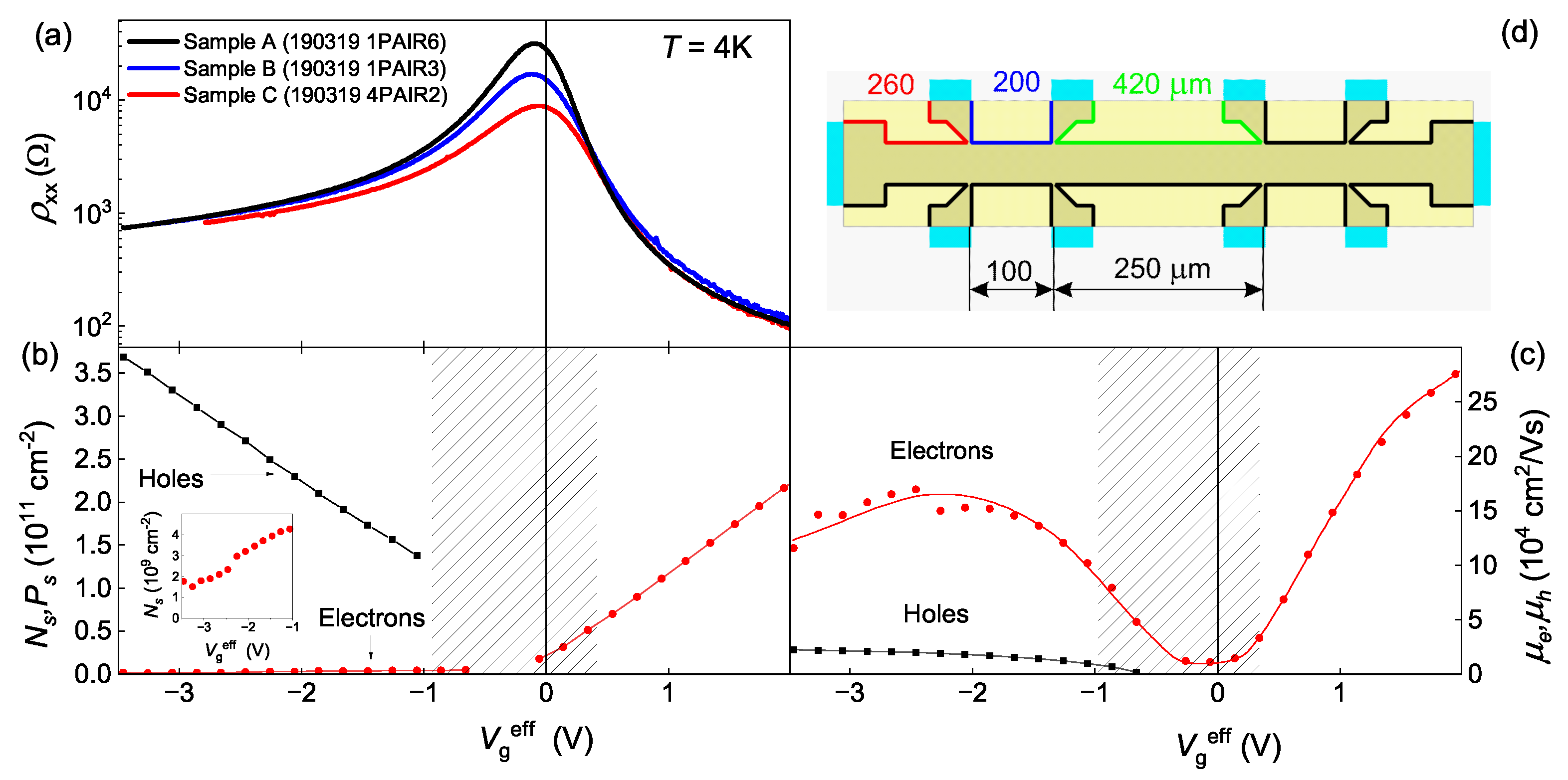
2. Samples
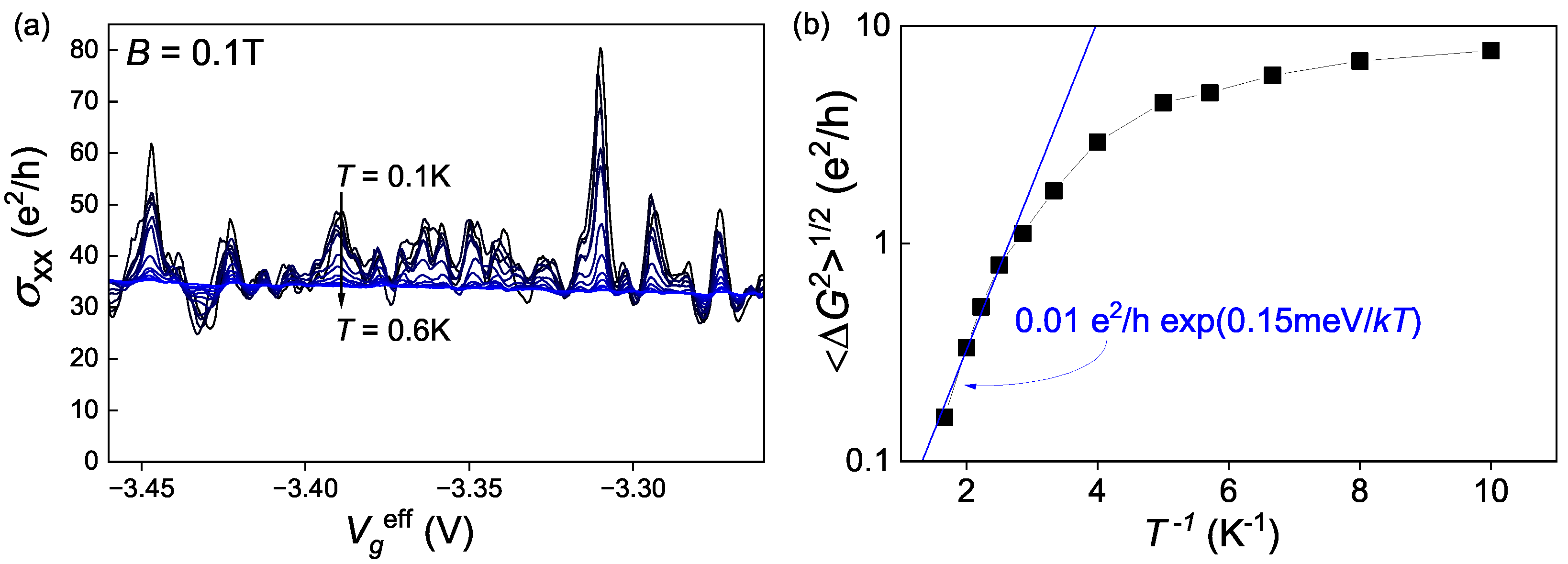
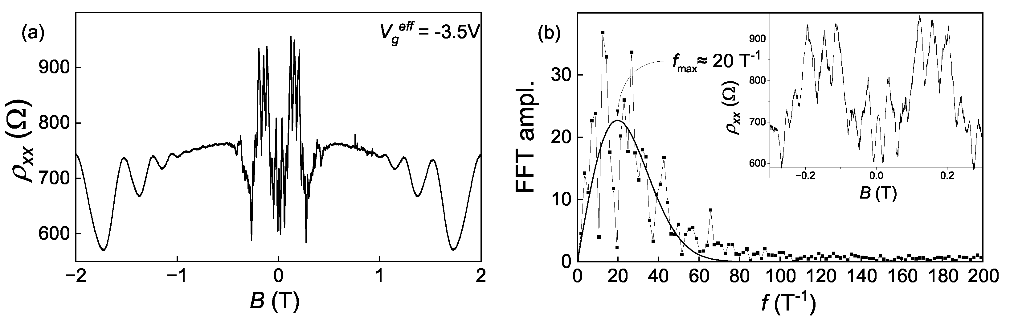
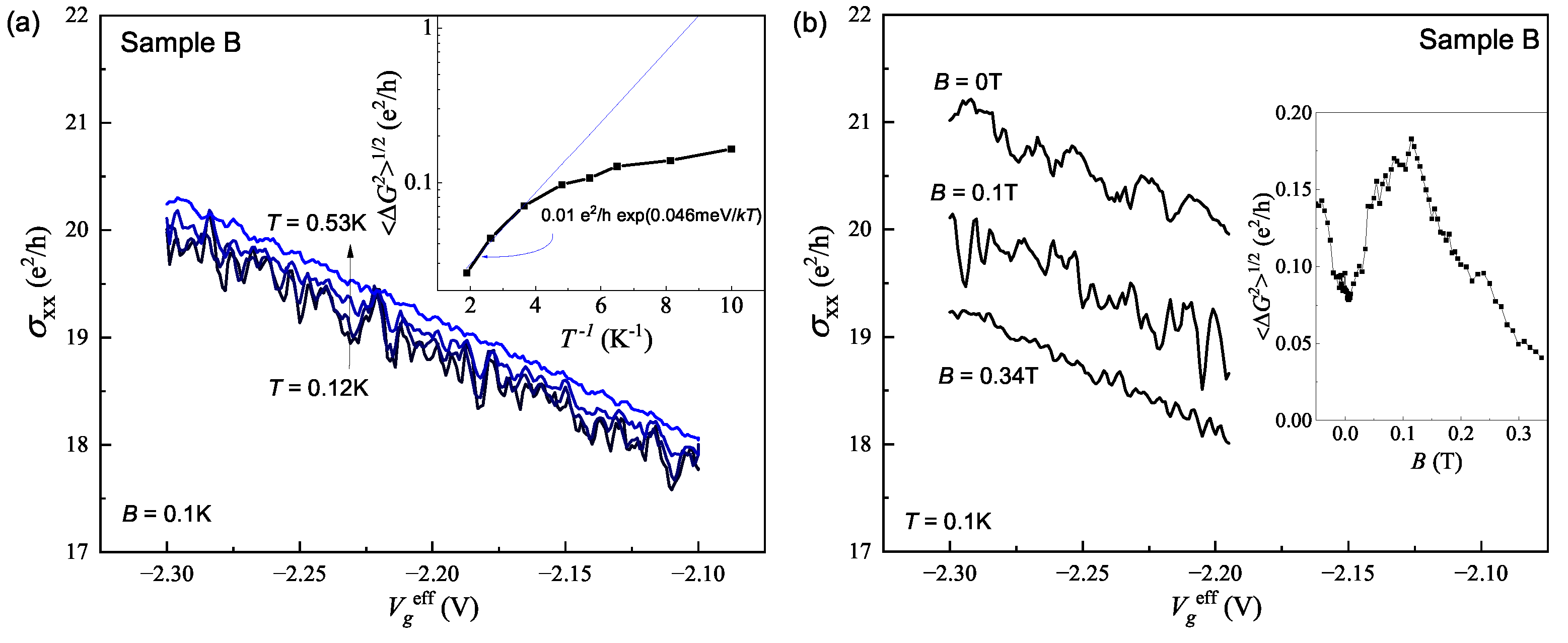
3. Results
4. Discussion
4.1. The Nature of Fluctuations
4.2. Qualitative Model of the Transport
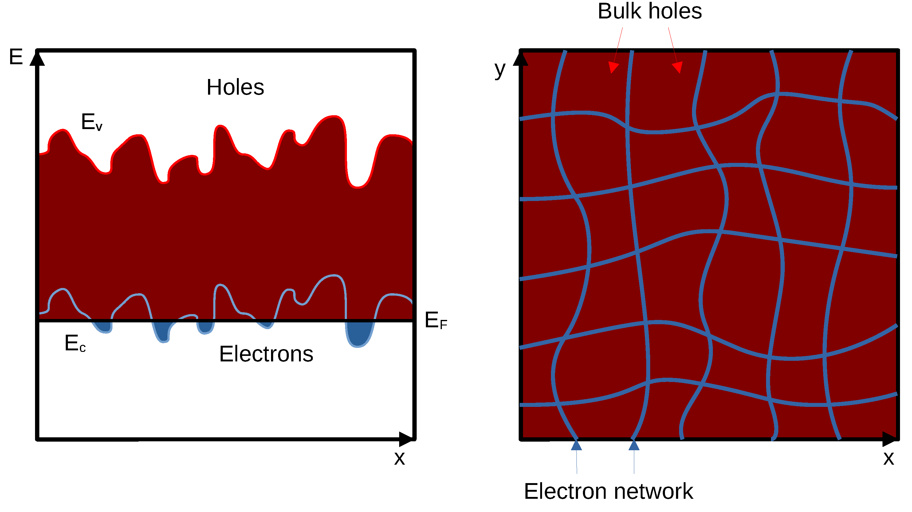
- Firstly, as has already been discussed, we assume that in the presence of impurities and heavy holes, the electron subsystem forms a percolation network. It could be similar to the squared network of electrons from References [45,46,47], but much less ordered. The fact that the formation of the percolation network crucially depends on a random potential of impurities explains the difference in the fluctuations amplitudes of samples A, B, and C with different levels of disorder. The question of how such a network actually forms we will leave to future theoretical studies;
- Secondly, we make the assumption that at low temperatures, the electron and hole subsystems are independent, while at higher temperatures, they exhibit strong interactions. Indeed, the electron-hole scattering is present in HgTe semimetals, resulting in a resistivity increase proportional to [48]. It also appears that direct transitions of an electron between the conduction and valence bands, which could even be present at zero temperature, are suppressed due to the significant distance between the electron and hole subbands in the momentum space. Conversely, electron-hole scattering occurs as an electron and a hole undergo momentum changes within their own subbands;
- Thirdly, we assume that the potentiometric contacts are connected to the electron subsystem. As illustrated in Figure 1d, the gate covers the sample, but the contacts are only partially covered. This implies that the Fermi energy in the areas not under the gate corresponds to a gate voltage of zero, which, for all three samples, corresponds to the electron band scenario. Since the contacts contain only electrons, and given that at low temperatures, the electron and hole subsystems do not interact, the potentiometric contacts provide potentials of exclusively electron subsystems. Furthermore, since the current contacts have a larger area than the potentiometric contacts (see Figure 1d), we can also assume that the potentials of the subsystems would be balanced, allowing the current to be carried by both electrons and holes.
5. Conclusions
Author Contributions
Funding
Data Availability Statement
Conflicts of Interest
Abbreviations
| UCF | Universal conductance fluctuations |
| QW | Quantum well |
References
- Altshuler, B.L. Fluctuations in the extrinsic conductivity of disordered conductors. Sov. J. Exp. Theor. Phys. Lett. 1985, 41, 530–533. [Google Scholar]
- Lee, P.A.; Stone, D.A. Universal conductance fluctuations in metals. Phys. Rev. Let. 1985, 55, 1622–1625. [Google Scholar] [CrossRef] [PubMed]
- Altshuler, B.L.; Khmelnitsky, D.E. Fluctuation properties of small conductors. Sov. J. Exp. Theor. Phys. Lett. 1985, 42, 359. [Google Scholar]
- Lee, P.A.; Stone, A.D.; Fukuyama, H. Universal conductance fluctuations in metals: Effects of finite temperature, interactions, and magnetic field. Phys. Rev. B 1987, 35, 1039. [Google Scholar] [CrossRef]
- Imry, Y. Introduction to Mesoscopic Physics; Oxford University Press Inc.: New York, NY, USA, 2002. [Google Scholar]
- Neuttiens, G.; Strunk, C.; Haesendonck, C.V.; Bruynseraede, Y. Universal conductance fluctuations and low-temperature 1/f noise in mesoscopic AuFe spin glasses. Phys. Rev. B 2000, 62, 3905. [Google Scholar] [CrossRef]
- Imamura, T.; Hikami, K. Mesoscopic Fluctuations in Superconducting Wires. J. Phys. Soc. Jpn. 2001, 70, 3312–3321. [Google Scholar] [CrossRef]
- Kasai, S.; Niiyama, T.; Saitoh, E.; Miyajima, H. Aharonov-Bohm oscillation of resistance observed in a ferromagnetic Fe-Ni nanoring. Appl. Phys. Lett. 2002, 81, 316–318. [Google Scholar] [CrossRef]
- Hara, M.; Endo, A.; Katsumoto, S.; Iye, Y. Universal Conductance Fluctuations in a Narrow Channel of Two-dimensional Electron Gas under Gradient Magnetic Field with Zero Mean. J. Phys. Soc. Jpn. 2004, 73, 2928–2931. [Google Scholar] [CrossRef]
- Spivak, B.; Zyuzin, A.; Cobden, D.H. Mesoscopic Oscillations of the Conductance of Disordered Metallic Samples as a Function of Temperature. Phys. Rev. Lett. 2005, 95, 226804. [Google Scholar] [CrossRef]
- Skvortsov, M.A.; Feigel’man, M.V. Superconductivity in Disordered Thin Films: Giant Mesoscopic Fluctuations. Phys. Rev. Lett. 2005, 95, 057002. [Google Scholar] [CrossRef]
- Adam, S.; Kindermann, M.; Rahav, S.; Brouwer, P.W. Mesoscopic anisotropic magnetoconductance fluctuations in ferromagnets. Phys. Rev. B 2006, 73, 212408. [Google Scholar] [CrossRef]
- Tagliacozzo, A.; Born, D.; Stornaiuolo, D.; Gambale, E.; Dalena, D.; Lombardi, F.; Barone, A.; Altshuler, B.L.; Tafuri, F. Observation of mesoscopic conductance fluctuations in YBa2Cu3O7-δ grain boundary Josephson junctions. Phys. Rev. B 2007, 75, 012507. [Google Scholar] [CrossRef]
- Blömers, C.; Schäpers, T.; Richter, T.; Calarco, R.; Lüth, H.; Marso, M. Phase-coherent transport in InN nanowires of various sizes. Phys. Rev. B 2008, 77, 201301. [Google Scholar] [CrossRef]
- Jespersen, T.S.; Polianski, M.L.; Sørensen, C.B.; Flensberg, K.; Nygård, J. Mesoscopic conductance fluctuations in InAs nanowire-based SNS junctions. New J. Phys. 2009, 11, 113025. [Google Scholar] [CrossRef]
- Alagha, S.; Hernández, S.E.; Blömers, C.; Stoica, T.; Calarco, R.; Schäpers, T. Universal conductance fluctuations and localization effects in InN nanowires connected in parallel. J. Appl. Phys. 2010, 108, 113704. [Google Scholar] [CrossRef]
- Liu, B.; Akis, R.; Ferry, D.K. Conductance fluctuations in semiconductor nanostructures. J. Condens. Matter Phys. 2013, 25, 395802. [Google Scholar] [CrossRef]
- Elm, M.T.; Uredat, P.; Binder, J.; Ostheim, L.; Schäfer, M.; Hille, P.; Müßener, J.; Schörmann, J.; Eickhoff, M.; Klar, P.J. Doping-Induced Universal Conductance Fluctuations in GaN Nanowires. Nano Lett. 2015, 15, 7822–7828. [Google Scholar] [CrossRef]
- Ioselevich, P.A.; Ostrovsky, P.M.; Fominov, Y.V. Mesoscopic supercurrent fluctuations in diffusive magnetic Josephson junctions. Phys. Rev. B 2018, 98, 144521. [Google Scholar] [CrossRef]
- Pessoa, N.L.; Barbosa, A.L.R.; Vasconcelos, G.L.; Macedo, A.M.S. Multifractal magnetoconductance fluctuations in mesoscopic systems. Phys. Rev. E 2021, 104, 054129. [Google Scholar] [CrossRef]
- Rycerz, A.; Tworzydło, J.; Beenakker, C.W.J. Anomalously large conductance fluctuations in weakly disordered graphene. Europhys. Lett. 2007, 79, 57003. [Google Scholar] [CrossRef]
- Kechedzhi, K.; Kashuba, O.; Fal’ko, V.I. Quantum kinetic equation and universal conductance fluctuations in graphene. Phys. Rev. B 2008, 77, 193403. [Google Scholar] [CrossRef]
- Staley, N.E.; Puls, C.P.; Liu, Y. Suppression of conductance fluctuation in weakly disordered mesoscopic graphene samples near the charge neutral point. Phys. Rev. B 2008, 77, 155429. [Google Scholar] [CrossRef]
- Kharitonov, M.Y.; Efetov, K.B. Universal conductance fluctuations in graphene. Phys. Rev. B 2008, 78, 033404. [Google Scholar] [CrossRef]
- Horsell, D.W.; Savchenko, A.K.; Tikhonenko, F.V.; Kechedzhi, K.; Lerner, I.V.; Fal’ko, V.I. Mesoscopic conductance fluctuations in graphene. Solid State Commun. 2009, 149, 1041–1045. [Google Scholar] [CrossRef]
- Bohra, G.; Somphonsane, R.; Aoki, N.; Ochiai, Y.; Ferry, D.K.; Bird, J.P. Robust mesoscopic fluctuations in disordered graphene. Appl. Phys. Lett. 2012, 101, 093110. [Google Scholar] [CrossRef]
- Bohra, G.; Somphonsane, R.; Aoki, N.; Ochiai, Y.; Akis, R.; Ferry, D.K.; Bird, J.P. Non-Ergodicity & Microscopic Symmetry Breaking of the Conductance Fluctuations in Disordered Mesoscopic Graphene. Phys. Rev. B 2012, 86, 161405. [Google Scholar]
- Minke, S.; Bundesmann, J.; Weiss, D.; Eroms, J. Phase coherent transport in graphene nanoribbons and graphene nanoribbon arrays. Phys. Rev. B 2012, 86, 155403. [Google Scholar] [CrossRef]
- Bao, R.; Huang, L.; Lai, Y.-C.; Grebogi, C. Conductance fluctuations in chaotic bilayer graphene quantum dots. Phys. Rev. E 2015, 92, 012918. [Google Scholar] [CrossRef]
- Terasawa, D.; Fukuda, A.; Fujimoto, A.; Ohno, Y.; Kanai, Y.; Matsumoto, K. Universal Conductance Fluctuation Due to Development of Weak Localization in Monolayer Graphene. Phys. Status Solidi B 2019, 256, 1800515. [Google Scholar] [CrossRef]
- Peng, H.; Lai, K.; Kong, D.; Meister, S.; Chen, Y.; Qi, X.-L.; Zhang, S.-C.; Shen, Z.-X.; Cui, Y. Aharonov–Bohm interference in topological insulator nanoribbons. Nat. Mater. 2009, 9, 225–229. [Google Scholar] [CrossRef]
- Matsuo, S.; Koyama, T.; Shimamura, K.; Arakawa, T.; Nishihara, Y.; Chiba, D.; Kobayashi, K.; Ono, T.; Chang, C.-Z.; He, K.; et al. Weak antilocalization and conductance fluctuation in a submicrometer-sized wire of epitaxial Bi2Se3. Phys. Rev. B 2012, 85, 075440. [Google Scholar] [CrossRef]
- Hamdou, B.; Gooth, J.; Dorn, A.; Pippel, E.; Nielsch, K. Aharonov-Bohm oscillations and weak antilocalization in topological insulator Sb2Te3 nanowires. Appl. Phys. Lett. 2013, 102, 223110. [Google Scholar] [CrossRef]
- Matsuo, S.; Chida, K.; Chiba, D.; Ono, T.; Slevin, K.; Kobayashi, K.; Ohtsuki, T.; Chang, C.-Z.; He, K.; Ma, X.-C.; et al. Experimental proof of universal conductance fluctuation in quasi-one-dimensional epitaxial Bi2Se3 wires. Phys. Rev. B 2013, 88, 155438. [Google Scholar] [CrossRef]
- Choe, D.-H.; Chang, K.J. Universal Conductance Fluctuation in Two-Dimensional Topological Insulators. Sci. Rep. 2015, 5, 10997. [Google Scholar] [CrossRef]
- Bhattacharyya, B.; Sharma, A.; Awana, V.P.S.; Srivastava, A.K.; Senguttuvan, T.D.; Husale, S. Observation of quantum oscillations in FIB fabricated nanowires of topological insulator (Bi2Se3). J. Condens. Matter Phys. 2017, 29, 115602. [Google Scholar] [CrossRef]
- Islam, S.; Bhattacharyya, S.; Nhalil, H.; Elizabeth, S.; Ghosh, A. Universal conductance fluctuations and direct observation of crossover of symmetry classes in topological insulators. Phys. Rev. B 2018, 97, 241412. [Google Scholar] [CrossRef]
- Mal, P.; Das, B.; Lakhani, A.; Bera, G.; Turpu, G.R.; Wu, J.-C.; Tomy, C.V.; Das, P. Unusual Conductance Fluctuations and Quantum Oscillation in Mesoscopic Topological Insulator PbBi4Te7. Sci. Rep. 2019, 9, 7018. [Google Scholar] [CrossRef]
- Mallick, D.; Mandal, S.; Ganesan, R.; Anil Kumar, P.S. Existence of electron–hole charge puddles and the observation of strong universal conductance fluctuations in a 3D topological insulator. Appl. Phys. Lett. 2021, 119, 013105. [Google Scholar] [CrossRef]
- Marinho, M.; Vieira, G.; Micklitz, T.; Schwiete, G.; Levchenko, A. Mesoscopic fluctuations in superconductor-topological insulator Josephson junctions. Ann. Phys. 2022, 447, 168978. [Google Scholar] [CrossRef]
- Huang, S.-M.; Lin, C.; You, S.-Y.; Yan, Y.-J.; Yu, S.-H.; Chou, M. The quantum oscillations in different probe configurations in the BiSbTe3 topological insulator macroflake. Sci. Rep. 2022, 12, 5191. [Google Scholar] [CrossRef]
- Vasil’ev, N.N.; Kvon, Z.D.; Mikhailov, N.N.; Ganichev, S.D. Two-Dimensional Semimetal HgTe in 14-nm-Thick Quantum Wells. Sov. J. Exp. Theor. Phys. Lett. 2021, 113, 466–470. [Google Scholar] [CrossRef]
- Kvon, Z.D.; Olshanetsky, E.B.; Drofa, M.A.; Mikhailov, N.N. Anderson Localization in a Two-Dimensional Electron–Hole System. Sov. J. Exp. Theor. Phys. Lett. 2021, 114, 341–346. [Google Scholar] [CrossRef]
- Gospodarič, J.; Shuvaev, A.; Mikhailov, N.N.; Kvon, Z.D.; Novik, E.G.; Pimenov, A. Energy spectrum of semimetallic HgTe quantum wells. Phys. Rev. B 2021, 104, 115307. [Google Scholar] [CrossRef]
- Umbach, C.P.; Van Haesendonck, C.; Laibowitz, R.B.; Washburn, S.; Webb, R.A. Direct observation of ensemble averaging of the Aharonov-Bohm effect in normal-metal loops. Phys. Rev. Let. 1986, 56, 386–389. [Google Scholar] [CrossRef] [PubMed]
- Ferrier, M.; Angers, L.; Rowe, A.C.H.; Guéron, S.; Bouchiat, H.; Texier, C.; Montambaux, G.; Mailly, D. Direct measurement of the phase-coherence length in a GaAs/GaAlAs square network. Phys. Rev. Let. 2004, 93, 246804. [Google Scholar] [CrossRef]
- Ferrier, M.; Rowe, A.C.H.; Guéron, S.; Bouchiat, H.; Texier, C.; Montambaux, G. Geometrical dependence of decoherence by electronic interactions in a GaAs/GaAlAs square network. Phys. Rev. Let. 2008, 100, 146802. [Google Scholar] [CrossRef]
- Kvon, Z.D.; Olshanetsky, E.B.; Kozlov, D.A.; Novik, E.; Mikhailov, N.N.; Dvoretsky, S.A. Two-dimensional semimetal in HgTe-based quantum wells. Low Temp. Phys. 2011, 37, 202–209. [Google Scholar] [CrossRef]


Disclaimer/Publisher’s Note: The statements, opinions and data contained in all publications are solely those of the individual author(s) and contributor(s) and not of MDPI and/or the editor(s). MDPI and/or the editor(s) disclaim responsibility for any injury to people or property resulting from any ideas, methods, instructions or products referred to in the content. |
© 2023 by the authors. Licensee MDPI, Basel, Switzerland. This article is an open access article distributed under the terms and conditions of the Creative Commons Attribution (CC BY) license (https://creativecommons.org/licenses/by/4.0/).
Share and Cite
Khudaiberdiev, D.; Kvon, Z.D.; Entin, M.V.; Kozlov, D.A.; Mikhailov, N.N.; Ryzhkov, M. Mesoscopic Conductance Fluctuations in 2D HgTe Semimetal. Nanomaterials 2023, 13, 2882. https://doi.org/10.3390/nano13212882
Khudaiberdiev D, Kvon ZD, Entin MV, Kozlov DA, Mikhailov NN, Ryzhkov M. Mesoscopic Conductance Fluctuations in 2D HgTe Semimetal. Nanomaterials. 2023; 13(21):2882. https://doi.org/10.3390/nano13212882
Chicago/Turabian StyleKhudaiberdiev, Daniiar, Ze Don Kvon, Matvey V. Entin, Dmitriy A. Kozlov, Nikolay N. Mikhailov, and Maxim Ryzhkov. 2023. "Mesoscopic Conductance Fluctuations in 2D HgTe Semimetal" Nanomaterials 13, no. 21: 2882. https://doi.org/10.3390/nano13212882
APA StyleKhudaiberdiev, D., Kvon, Z. D., Entin, M. V., Kozlov, D. A., Mikhailov, N. N., & Ryzhkov, M. (2023). Mesoscopic Conductance Fluctuations in 2D HgTe Semimetal. Nanomaterials, 13(21), 2882. https://doi.org/10.3390/nano13212882