Abstract
In recent years, scientists have conducted extensive research on Moiré materials and have discovered some compelling properties. The Moiré superlattice allows superconductivity through flat-band and strong correlation effects. The presence of flat bands causes the Moiré material to exhibit topological properties as well. Modulating electronic interactions with magnetic fields in Moiré materials enables the fractional quantum Hall effect. In addition, Moiré materials have ferromagnetic and antiferromagnetic properties. By tuning the interlayer coupling and spin interactions of the Moiré superlattice, different magnetic properties can be achieved. Finally, this review also discusses the applications of Moiré materials in the fields of photocurrent, superconductivity, and thermoelectricity. Overall, Moiré superlattices provide a new dimension in the development of two-dimensional materials.
1. Introduction
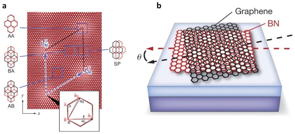
Two-dimensional materials have garnered significant interest due to their unique physical properties following the discovery of graphene in 2004 [1]. These materials are stacked together to form different kinds of homo- or heterostructures through van der Waals (vdW) interactions [2,3,4,5,6,7,8]. VdW materials, on the other hand, are those in which van der Waals forces form between layers [5,9,10,11,12]. These interactions lead to the formation of heterojunctions, enriching the performance of 2D materials as various novel physical and chemical properties manifest themselves [13,14,15]. The periodic Moiré pattern is formed when two 2D sheets are stacked and rotated at a specific angle [16]. Moiré superlattice is a heterostructure formed by lattices mismatching or interlayer twisting [17,18,19,20]. As shown in Figure 1, the materials involved can be identical, as seen in twisted bilayer graphene (TBG), or they can be different materials, such as graphene on hexagonal boron nitride (h-BN) [16,18,21,22,23,24]. By artificially rotating one single graphene with another single graphene at a small specific angle, a twisted bilayer graphene is formed, resulting in a low-energy van Hove singularity [25,26,27]. In graphene-h-BN heterostructures, h-BN helps enhance the carrier mobility of graphene by suppressing charge inhomogeneities [28,29]. A periodic superlattice causes the band gap at the Dirac point of graphene to open, [30,31,32] resulting in several unusual quantum phenomena, including the quantum Hall effect and the Hofstadter butterfly pattern. This is a noteworthy advancement in the field [16,33,34]. The atomic and electronic structure of vdW heterostructures is subject to periodic modulation by Moiré superlattices (MSLs), leading to the appearance of several phenomena such as the formation of shear solitons and topological point defects [35,36,37,38], secondary Dirac cones [39,40,41], and Hofstadter butterfly states [33,42,43,44]. In addition, flat bands were discussed back in 2011; such flat energy bands are of interest and may localize the presence of electronic states. Related insulator behavior is found, and unconventional superconductivity is found in a TBG of approximately 1.1° [45,46,47]. Visualization of flat bands by using angle-resolved photoemission spectroscopy with nanoscale resolution (nanoARPES) was reported in 2021 [48,49].

Figure 1.
Moiré superlattice. (a) Schematic of twisted bilayer graphene [18]. (b) Schematic of twisted graphene/BN [16].
The Moiré superlattice offers new opportunities for the development of two-dimensional materials, providing new dimensions in scientific research in the areas of force, thermal, optical, and electrical fields. This comprehensive review discusses the properties and diverse applications of Moiré materials, encompassing superconductivity, the fractional quantum Hall effect, ferromagnetism, antiferromagnetic, and the topological characteristics of Moiré superlattices. Additionally, it explores the versatile utilization of Moiré materials in photocurrent devices, superconducting quantum interferometry devices, mechanical flexibility, and thermoelectric applications.
2. Properties
2.1. Superconductivity of Moiré Superlattice
The formation of an electronic flat band can stem from various sources, including topological factors, symmetry considerations, and interactions [50,51]. In the case of graphene layer twisting, the topological mechanism is responsible for the flat band formation. Another reason for the emergence of a nearly flat band may be the spontaneous development of a misfit dislocation array at the interface. The topological aspect of this flat band can also be explained in terms of the pseudo-magnetic field generated by strain [52]. These topologically protected band-touching lines in the graphite spectrum, [53] known as Dirac lines, result in an approximately flat band on the surface of graphite or at the interface. Flat bands offer distinct advantages due to their ability to ensure a high density of states, which enhances the impact of interactions. Consequently, superconductivity induced by electronic correlations becomes apparent at temperatures that are remarkably close to room temperature [54].
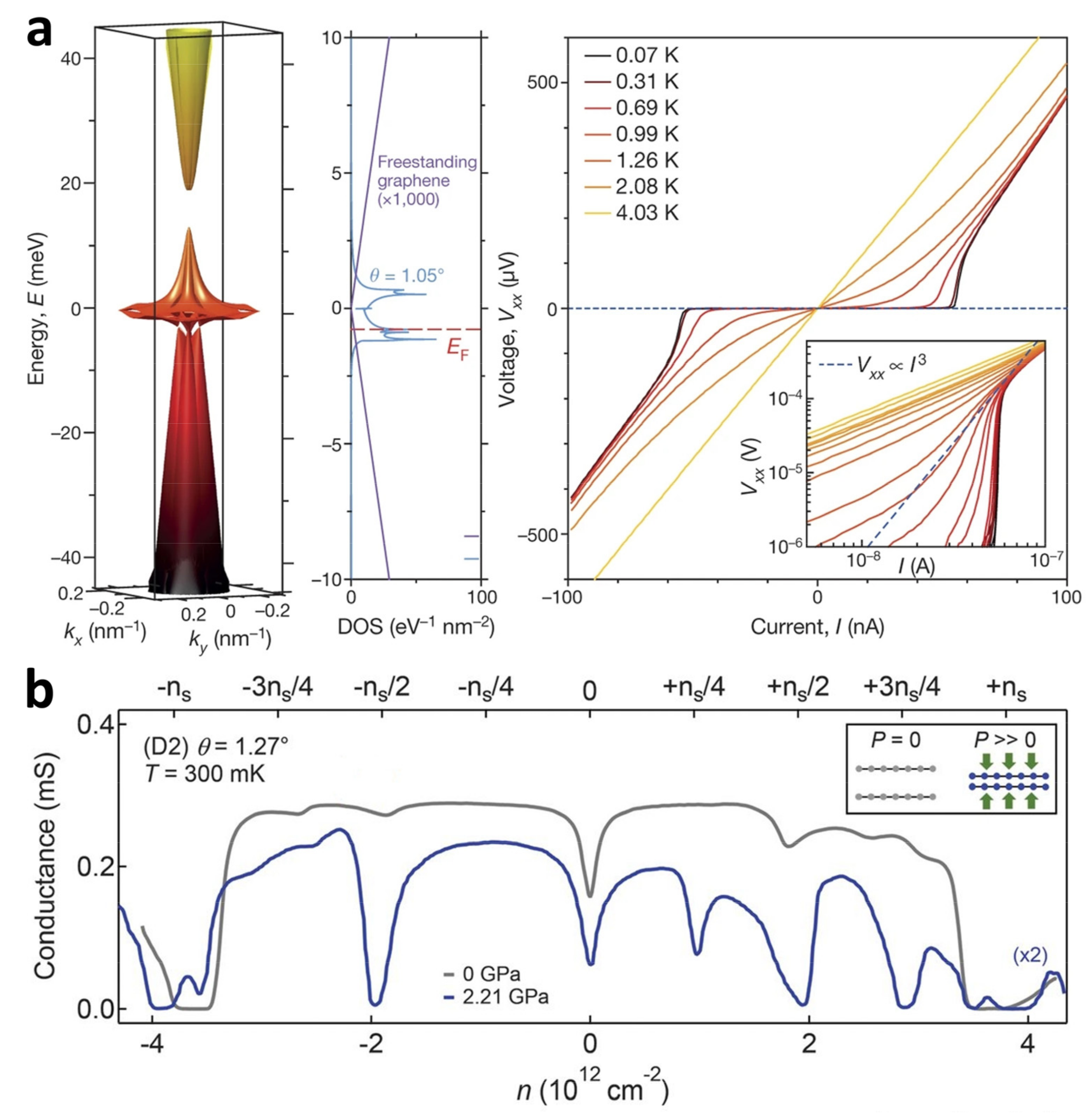
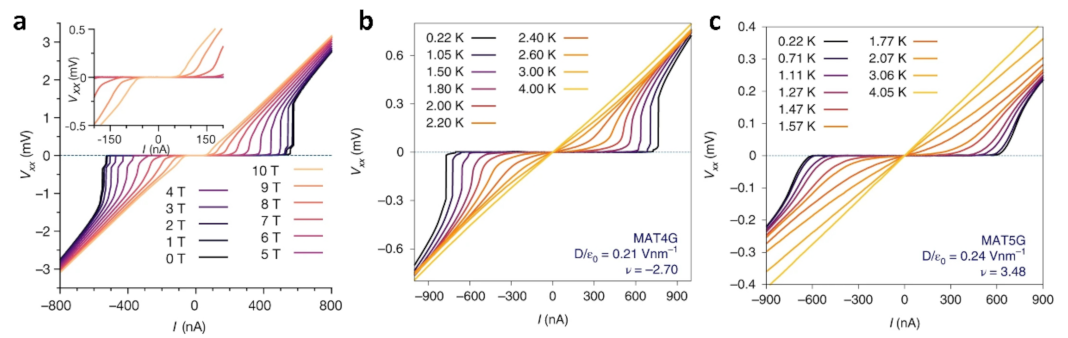
Twisting two monolayer graphene sheets to a specific angle while applying an electric field to control charge density can induce superconductivity at low temperatures. This discovery has ignited global interest in researching twisted-angle graphene systems [46]. In Figure 2a, the device exhibits superconductivity when the Fermi energy of the TBG with θ = 1.05° approaches half of the filling of the lower flat band. The flat-band energy level exhibits energy levels that are over 1000 times greater than the energy levels of two separate, unconnected graphene sheets. This phenomenon occurs as a result of reduced Fermi velocity and increased localization near the magic angle. In Figure 2a, when examining the I–Vxx curves of devices with an angle of θ = 1.05° at various temperatures, it is evident that they exhibit the characteristics of a 2D superconductor. Notably, the curve shows a critical current of about 50 nA at temperatures as low as 70 mK. The electrical conductivity plotted against the density of electron holes for a TBG device featuring a twist angle of θ = 1.27° is displayed in Figure 2b. The strong insulating state at 0 GPa appears at ±ns of the fully filled Moiré cell, indicating the existence of an isolated low-energy band. The feeble insulating states are shown near ±ns/2 and ±3ns/4, and there is no indication of superconductivity. These observations suggest that the low energy band is not significantly involved at this angle. The insulating state becomes apparent at several reasonable fillings of the molar unit cell at 2.21 GPa, most notably at ±ns/2 and +3ns/4, and even weaker at +ns/4. In Figure 3a, the evolution of the Vxx–I (voltage–current) curve as a function of B∥ for twisted three–layer graphene (θ = 1.57°, with adjacent layers sequentially twisted by θ and −θ) shows the robustness of superconductivity (i.e., not the low resistance in the normal state). Despite the fact that the critical current shows a gradual decrease as the parallel magnetic field (B∥) increases, it is evident that when B∥ reaches 10 T, the Vxx–I graph still displays a significantly level region for a given DC current bias, suggesting the absence of resistance. However, a sudden increase can be observed in the differential resistance at the critical current. Sharp switching behavior in the V–I curves of twisted four-layer graphene (T4G) and twisted five-layer graphene (T5G) confirms true, robust superconductivity (Figure 3b,c).
Figure 2.
(a) TBG (θ = 1.05°) energy band and the corresponding DOS. Measured Vxx–I curves for devices at different temperatures [46]. (b) The conductivity of TBG (θ = 1.27°) is modulated by the pressure modulation results. The inset shows the effect of pressure on the interlayer distance [55].
Figure 3.
(a) Vxx–I curves for T3G modulated by in-plane magnetic fields [56]. (b,c) Vxx–I curves for T4G and T5G at different temperatures [57].
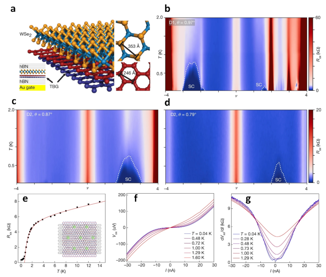
Figure 4a shows a device made from an hBN-TBG-WSe2-hBN van der Waals stack, where the WSe2 monolayer is located between the top hBN and TBG instead of the usual hBN-TBG-hBN structure. In Figure 4b–d, the temperature dependence of the resistances of the TBG-WSe2 structures (θ = 0.97°, θ = 0.87° and θ = 0.79°) shows superconductivity. The trilayer graphene/hBN Moiré superlattice shows a significant decrease in resistance over a small temperature range (Figure 4e). At the lowest temperature, the I–V curve demonstrates a critical current of less than 10 nA, while at higher temperatures, it shows a near-linear behavior. The differential resistance in Figure 4g highlights a critical current of approximately 10 nA at temperatures below 0.3 K, which develops into normal metallic behavior at temperatures above about 1 K, progressing to normal metal behavior above approximately 1 K.

Figure 4.
(a) Diagram of the structure of TBG-WSe2, top view of WSe2 and graphene. (b–d) Relationship between resistance Rxx and temperature and electron density for the three twist angles [58]. (e) Rxx–T curve for trilayer graphene/hBN Moiré superlattice. (f) I–V curves of trilayer graphene/hBN at different temperatures. (g) dVxx/dI–I curves at different temperatures of trilayer graphene/hBN [59].
2.2. Fractional Quantum Hall Effect of Moiré Superlattice
At extremely low temperatures, a 2D electron gas exposed to a perpendicular magnetic field undergoes energy quantization into discrete Landau levels. In the presence of a strong magnetic field, the Hall conductance exhibits a quantum plateau as the field strength varies. These plateaus exist near the filling factor of the Landau energy level by an integer or a specific fraction and are known as the integer or fractional quantum Hall effect. The investigation of topological states originated from the experimental observation of fractional quantum Hall effects in 1982, as reported in reference [60].
The fractional quantum Hall effect, as a topological state due to inter-electron interaction, has attracted widespread interest due to its fractionalized quasiparticle excitation. Back in 2013, the quantum Hall effect of graphene was observed, and the fractional quantum Hall effect was discussed [34].
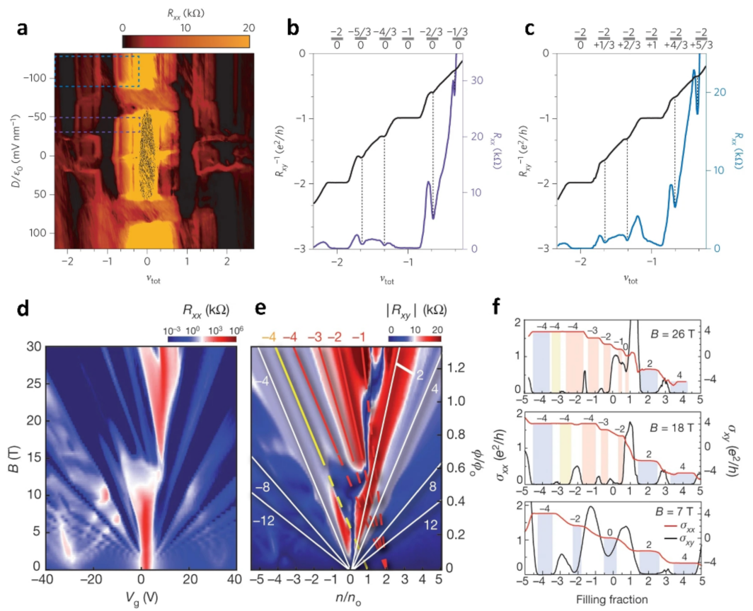
Figure 5a–c shows the Fractional quantum Hall effect in twisted bilayer graphene [61]. The Rxx at B = 9 T shows several significant minima (Figure 5a), while one graphene layer exhibits a ν = 0 insulating state (Figure 5b). A significant fractional quantum Hall effect was found in the electron–hole in the TBG. The detection of fractional quantum Hall states sets the foundation for achieving a fractional quantum spin Hall state, which is an essential component in current plans to create fractional versions of Majorana fermions [62,63,64]. Figure 5d–f shows the anomalous quantum Hall states of twist graphene/h-BN [16]. These are the results of a study on magnetic transport at high magnetic fields. The authors focus on the evolution of Rxx and Rxy at magnetic fields up to 31 T and plot these quantitative values on images of adjustable experimental gate voltages and magnetic fields, respectively, as well as on dimensionless parameters that appear in the Diophantine equation. They compare their results with those of conventional quantum Hall systems and find that at large magnetic fields, in addition to the usual sequence of bilayer graphene, several additional quantum Hall effect (QHE) states appear, which exhibit minimal values in Rxx and plateaus in Rxy and exhibit linear trajectories when plotted on the Landau sector diagram. These anomalous QHE states are characterized by integer-valued intercepts s and slopes t and are consistent with a fully developed spectral gap arising from a Hofstadter-type energy spectrum. The authors present conclusive proof that the quantum Hall effect properties related to the Hofstadter spectral gap can be identified by the intercept and slope quantum numbers in the Wannier diagram.

Figure 5.
(a) Rxx at B = 9 T as a function of νtot and D. (b) The Rxx and Rxy lines in the purple rectangular range in a. The result is a fractional state for the top layer and an insulating state for the bottom layer, respectively. (c) The Rxx and Rxy lines in the blue rectangular range in a. The data correspond to the electron–hole combination. The plotted lines in b and c are averages of the measured quantities over a range of D field values as indicated respectively by the purple and blue rectangles in the colourmap of a. (d) Resistance Rxx as a function of B(T) and Vg(V). (e) Resistance Rxy as a function of ϕ/ϕo and n/no. (f) Longitudinal and transverse Hall conductivity at different magnetic fields. Yellow and red bars indicate correspondence to the similarly coloured anomalous features marked by solid lines in d, e. Blue bars indicate the conventional QHE features.
The quantum Hall effect appears not only in twisted bilayer graphene but also in other Moiré materials, such as twisted ZrS2 heterostructures. The Moiré superlattice of twisted heterostructures of ZrS2 stacks in AA, AB, and BA (Figure 6a) [65]. Neglecting spin-orbit coupling, the valence bands degenerate at Γ in both the AA and AB regions. A very strong anomalous Hall effect appears, as shown in Figure 6b. The difference, however, is that it is not the same as the QHE in the TBG. This phenomenon relies on the intrinsically topologically non-trivial Moiré band structure because of spin-orbit coupling and avoids the simultaneous valley polarization and base effects.
Figure 6.
(a) Twisted heterostructures of ZrS2 and degradation of the electronic state. (b) Quantum anomalous Hall effect and fractional Chern insulators [65].
2.3. Ferromagnetic of Moiré Superlattice
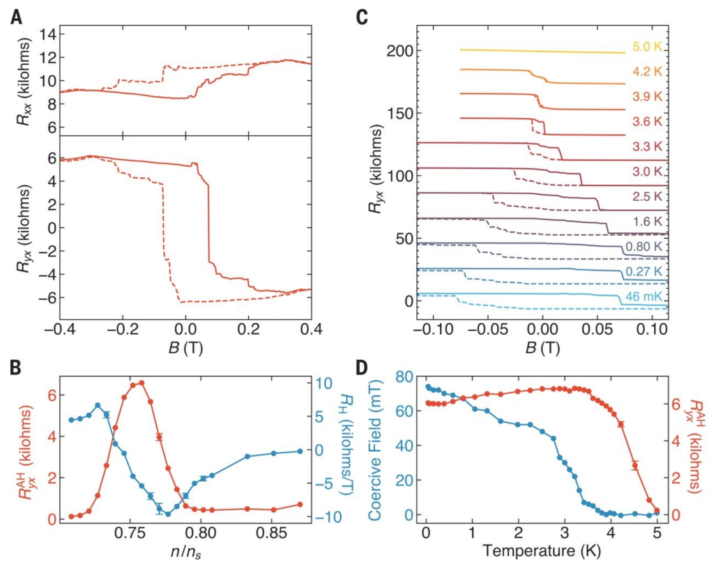
TBG experiences pronounced electron interactions at a specific angle [66,67,68]. At a particular electron density, magic angle graphene exhibits magnetic properties [69,70,71,72]. Theoretical calculations suggest that this magnetic behavior arises due to the interaction, which lifts spin and valley degeneracy. Typically, the magnetic transport in graphene heterostructures remains unaffected by an applied magnetic field. However, in Figure 7 [73], the magnetic field-dependent resistance in the TBG shows a remanence phenomenon (Figure 7A,B). The transport is hysteretic with respect to an applied out-of-plane magnetic field B (Figure 7A). This phenomenon is important because there are neither transition metals nor heavy elements in the TBG, and the response of the TBG to the magnetic field is related to the effect. The hysteresis loop closes when the temperature rises (Figure 7C,D).

Figure 7.
In TBG, (A) magnetic field dependent longitudinal resistance Rxx and Hall resistance Ryx. (B) AH resistance Ryx and RH as a function of n/ns. (C) Temperature-dependent Ryx as a function of B. (D) Coercive field and AH resistance Ryx as a function of temperature [73].
The ABC-TLG/hBN heterostructure offers a highly compelling platform for investigating interrelated topological phenomena [74,75,76,77,78]. Figure 8a shows the ABC-trilayer graphene/hexagonal boron nitride (ABC-TLG/hBN) moiré superlattice Hall bar device [79]. In Figure 8b, the graph depicts the Hall resistivity as a function of temperature while subjecting a minor perpendicular magnetic field to a sweeping range of −0.1 T to 0.1 T. Notably, the Hall resistivity exhibits a pronounced anomalous Hall signal accompanied by a robust ferromagnetic hysteresis. The correlated Chern insulator retains its properties even in the absence of a magnetic field, leading to the spontaneous violation of time-reversal symmetry. This state can also give rise to valley-flavor ferromagnetism when filled to one-fourth of its capacity. Notably, ferromagnetic behavior and significant anomalous Hall signals manifest in the Chern insulator state, even when no external magnetic field is applied.
Figure 8.
(a) Schematic of the ABC-trilayer graphene/hexagonal boron nitride (ABC-TLG/hBN) moiré superlattice Hall bar device. The inset shows that the moiré pattern exists between ABC-TLG and bottom hBN. (b) Magnetic-field-dependent ρyx at different temperatures [79].
2.4. Antiferromagnetic of Twisted Bilayer CrI3
In Moiré materials, Moiré superlattices are capable of generating new magnetic properties through interlayer coupling interactions [77,78,79,80,81]. The researchers found that the coexistence of ferromagnetism (FM) and antiferromagnetism (AF) occurs in twisted bilayers of CrI3 at small angles [78]. Three types of stacking appear in the twisted bilayer CrI3 (Figure 9a) [82]. The occurrence of the magic pattern results in the formation of a magnetic domain boundary separating the R and M regions. (Figure 9b). On the scale of the Moiré length, the competing interactions between interlayer antiferromagnetic and ferromagnetic forces can generate magnetic ground states that are non-trivial, featuring coexisting domains of antiferromagnetic and ferromagnetic properties [83]. At 1.2° ferromagnetism and antiferromagnetism coexist. As θ increases, AF behavior decreases. At 4°, there is small AF behavior; at 15°, there is only FM behavior (Figure 9c–f). Above the critical angle θc ≈ 3°, only the FM response is observed as the AF-FM coexistence disappears (Figure 9g). However, below θc, we observe that FM, Bc, and FM are all only slightly dependent on the angle.
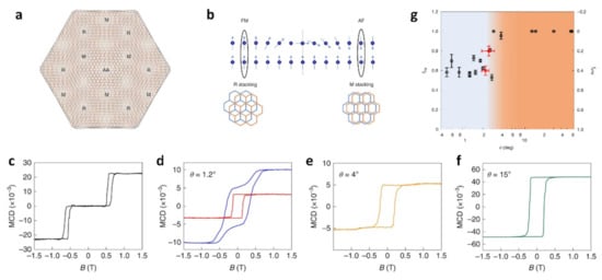
Figure 9.
(a) Schematic diagram of the twisted bilayer CrI3 structure. R, M, and AA are shorthand for these stacking methods, i.e., rhombohedral, monoclinic, and AA stacking. (b) The magnetic domain wall appears between R and M. (c–f) MCD microscopy of twist bilayer CrI3, where MCD of bilayer CrI3 is shown in a, and the red line in b is the MCD of a monolayer of CrI3. Black, blue, yellow and green lines indicate natural bilayer CrI3 (a) and twisted bilayer CrI3 with torsion angles of 1.2°, 4° and 15°, respectively. (g) Twist angle θ dependent AM and FM [82].
2.5. Topological of Twisted Monolayer-Bilayer Graphene
Understanding the quantum properties in crystalline solids hinges on grasping the fundamental concept of the topological phase of matter [84]. The topological classification hinges on the presence of an energy spectrum gap, with the topological invariant determined by how eigenstates below this gap vary concerning the Bloch wave number [85,86]. Quasicrystalline systems have garnered significant interest due to their topological characteristics. If two atomic layers are superimposed at an arbitrary rotation angle, it typically results in a lack of alignment between the periodic patterns of the individual layers, causing the entire system to exhibit quasiperiodic behavior. Expanding beyond the bilayer scenario, when the relative twist angles form rational ratios, a periodic pattern emerges in the quasimomentum space, resulting in moiré Bloch bands. This occurs even when the system lacks a crystalline lattice structure in real space [87]. One notable characteristic of these 2D twisted quasicrystals is their electronic structure, which can be systematically altered through adjustments in the twist angle or by introducing changes to the lattice structure of individual layers [88].
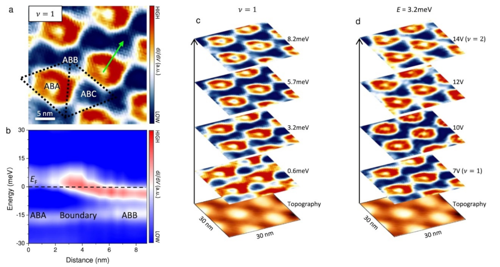
The lattice misalignment between layers of the vdH heterostructure can lead to the emergence of flat bands, a phenomenon that can be explored for related quantum phenomena [45,46,47]. The potential reduction of spatial symmetry when multi-layered graphene is twisted leads to topological non-trivial in flat bands [89,90,91]. Twisted monolayer-bilayer graphene (tMBG) possesses an inherent non-trivial band topology that distinguishes it from the Chern bands found in TBG [92,93]. The filling state of the conduction flat band (CFB) in tMBG with θ = 1.04° determines the topological properties of the system. The CFB filling is induced within the Moiré lattice, and accordingly, there is a change in the topological properties [94]. As shown in Figure 10a, ABB and ABA structures possess dissimilar topological characteristics in the vicinity of the Fermi energy level. Consequently, the density of states experiences a boost owing to the protection of topological boundaries (Figure 10b) [95,96]. An important point to note is that the radius of the circular structure remains constant regardless of changes in energy or doping (Figure 10c,d). This formation of ring structure originates from topologically protected boundary states. By combining a relevant driven electronic crystal with a ribbon-shaped topological structure, it is possible to create topologically protected states and lattice structures with circular geometry [94].
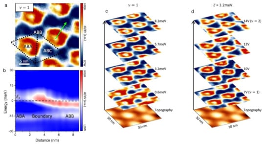
Figure 10.
(a) Plot of dI/dV at v = 1. (b)Variation of dI/dV intensity from ABA to ABB regions along the direction of the arrow in (a). (c) Variation of dI/dV with energy at ν = 1. (d) Plot of dI/dV at different doping for E = 3.2 meV [94].
3. Applications of Moiré Superlattices
3.1. Photocurrent of TBG Device
A new type of photodetector called scanning nanophotocurrent imaging has the ability to detect and pinpoint changes in the DC transport characteristics of graphene at the nanoscale level [97]. Small angles of TBG change the electronic properties due to interlayer coupling [98,99,100,101]. It is shown that bias modulation opens the band gap of graphene [102,103,104,105]. In TBG devices, researchers concentrate the infrared light onto the metal tip to amplify the electric field beneath it (Figure 11a) [97]. This amplified electric field produces a photocurrent in the local area, which we detect without applying any bias voltage. Photocurrents are produced in graphene as a result of the photoelectric effect (PTE) caused by variations in electron distribution [106,107,108]. The images in Figure 11c–e use red and blue colors to represent positive and negative currents, respectively, and white areas indicate zero current. The photocurrent image displays the intricate structure of the hexagonal lattice, which corresponds to the magnetic domain walls of the relaxed Mohr superlattice in the TBG. The charge neutral point (CNP) is visible when the gate voltage (VG) is +4 V. When comparing the results for gate voltages of −12 V and 14 V, the photocurrent exhibits a similar zigzag pattern for both positive and negative gate voltages, with the only difference being a change in sign. Figure 11f displays the photocurrent patterns acquired through hyperbolic tip calculations, which accurately replicate both the zigzag pattern and intricate details of the domain walls. The results reveal a correlation between the characteristics observed in the photocurrent images and those present in the Seebeck coefficients (Figure 11b). Specifically, the straight lines running along the y-axis and the zero-crossing contours are a result of the magnetic domain walls themselves, while the curved over-zero contour intersects with the magnetic zone wall, leading to interference from the photocurrent in the adjacent zone wall. These findings demonstrate that photocurrent experiments provide direct insight into the nanoscale variations of Seebeck coefficients within the domain walls.
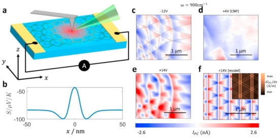
Figure 11.
(a) Schematic of the scanning photocurrent of a small angle TBG device. (b) Seebeck coefficient curves. (c–e) Illustration of photocurrent at different bias voltages. (f) The photocurrent pattern was computed utilizing the Shockley-Ramo formalism [97,109].
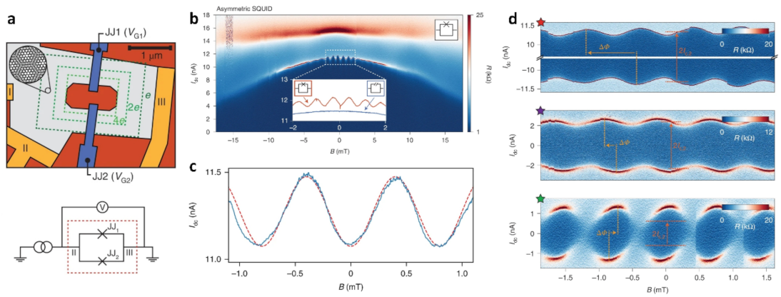
3.2. Superconducting Quantum Interference Device (SQUID)
Electrostatic doping is a viable method for adjusting numerous relevant material states of the Moiré superlattice [106]. Tunable Josephson junctions have been made possible by the existence of a range of in situ tunable states [110,111,112,113]. Despite the measurement of phase-coherent phenomena, there has been no demonstration of controlling the phase difference between the superconducting condensates thus far. On the basis of the implementation of gate control, a superconducting quantum interference device (SQUID) has been fabricated in TBG [111]. By electrostatic manipulation of the proximity current through the junction in SQUID, its properties can be adjusted (Figure 12a) [114]. At critical currents, oscillations are found, and the superconducting state can be tuned out by electrostatics to suppress the oscillations (Figure 12b). A reduction in the offset 2Ic,2 between the mean values of the positive and negative switching currents results in a change in symmetry from asymmetry to symmetry (Figure 12d). The current phase relationship (CPR) shows that the applied magnetic field and Idc are sinusoidal (Figure 12c).

Figure 12.
(a) Schematic diagram of the SQUI device and circuit equivalents. (b) Image of the resistance as a function of Idc and the magnetic field. The illustration shows the trajectory of the critical current line within the oscillation region. (c) The image of Idc as a function of the magnetic field showing the current phase relationship (CPR). (d) Magnetic interference patterns [114].
3.3. Moiré Superlattices Derived from Mechanical Flexibility
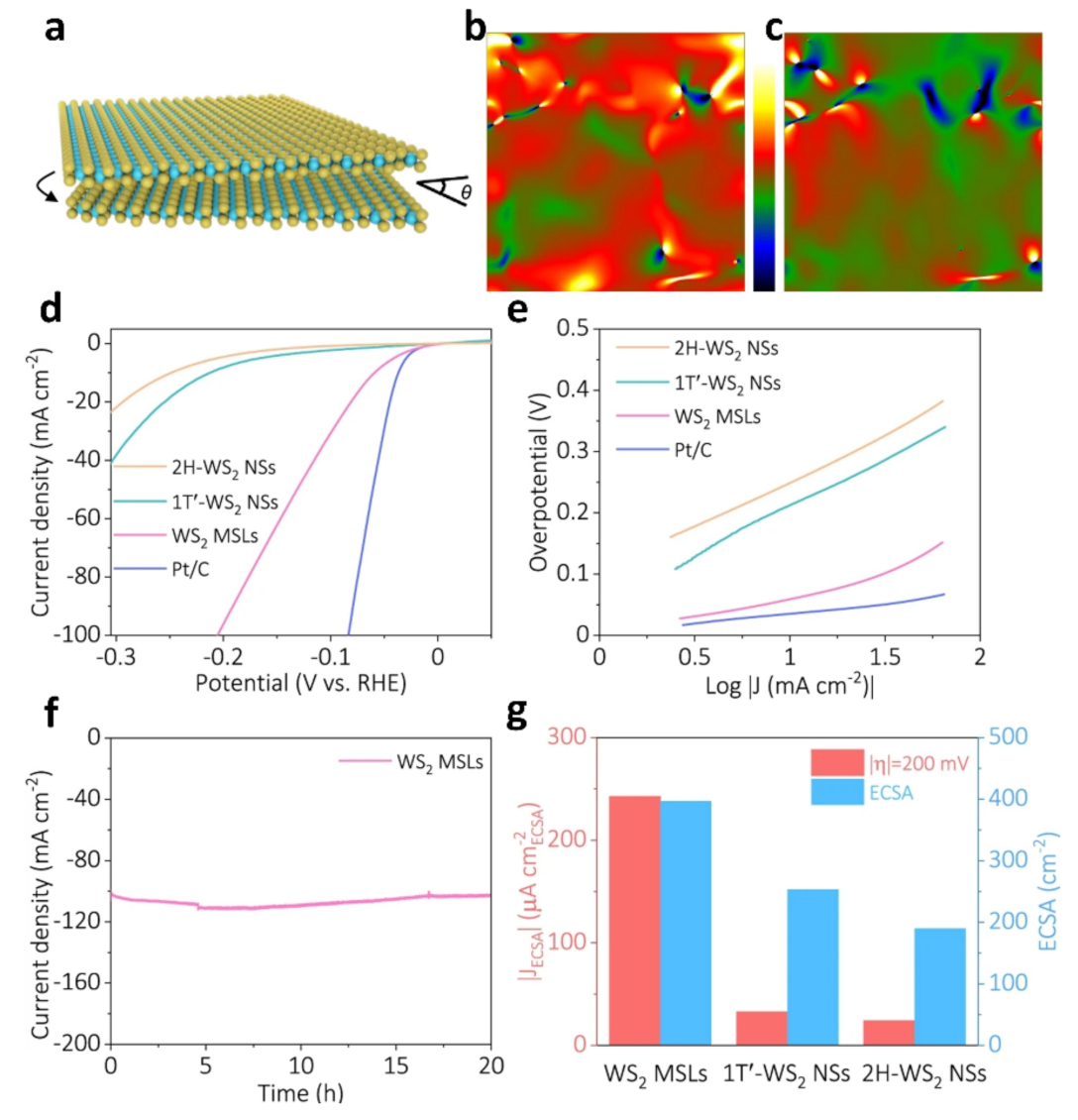
The conventional method of fabricating Moiré superlattices (MSLs) involves stacking materials together, which is highly demanding and requires stringent experimental conditions [115,116]. By applying mechanical strain between WS2 layers, a Moiré superlattice with periodic structures is formed. This superlattice structure significantly influences the hydrogen evolution reaction performance of WS2 catalysts. WS2 Moiré superlattices exhibit excellent catalytic activity and stability, effectively promoting the hydrogen evolution reaction. As illustrated in Figure 13a, the mechanical instability leads to S-W-S layer slippage, which in turn causes the formation of Moiré superlattices [117]. Figure 13b,c demonstrate the successful introduction of strain through topology engineering utilizing mechanical flexibility. Figure 13d reveals that the WS2 MSLs exhibit a remarkably low overpotential of only 60 mV vs. RHE at a current density of 10 mA cm−2, which is significantly superior to other WS2 samples. Figure 13e reveals that the Tafel slope implies that the hydrogen evolution reaction (HER) reaction of WS2 MSLs may exhibit a similar mechanism to Volmer–Heyrovsky and is strongly influenced by electrochemical desorption [118,119]. WS2 Moiré superlattices exhibit superior hydrogen evolution reaction performance. The results of a 20-h current duration test indicate that the stability of WS2 Moiré superlattices remains unaffected during this process. Electrochemically active surface area (ECSA) results reveal that WS2 Moiré superlattices possess a higher concentration of enriched activity.

Figure 13.
(a) WS2 Moiré superlattices. (b,c) Strain distributions of exx and exy, respectively. (The color from green to dark blue and the color from red to bright yellow represent the compressive strain and tensile strain, respectively). (d) Polarization curves of all catalysts. (e) The corresponding Tafel curves for catalysts derived from (d). (f) Continuous HER recorded from synthesized WS2 MSLs. (g) Comparison of the ECSA and JECSA [117].
3.4. Thermoelectric of Twist Bilayer Borophene
Twisted superlattices made of 2D materials frequently exhibit fascinating properties and can be tuned accordingly. In 2023, Song et al. conducted a theoretical investigation on 30° twisted α-bilayer borophene (TBB) and examined the feasibility of its synthesis (Figure 14) [120]. Twisting the α-bilayer borophene introduces unique interlayer charge-transfer interactions, where electrons are transferred from Ag to TBB. This electron transfer enhances the stability of TBB synthesis on an Ag substrate. Moreover, the act of twisting significantly enhances the thermoelectric performance of bilayer borophene. The inversion of the Seebeck coefficient is a result of the Dirac point splitting near the Γ point. Introducing a twisted superlattice enhances the Seebeck coefficient, increasing it from 300 to 500 μV/K, and raises the optimum temperature to approximately 110 K. Twisting the superlattice creates multiple quantum wells, effectively aligning the high conductivity and large Seebeck coefficient within the same range. The coexistence of large S (Seebeck coefficient) and σ (conductivity) in this region results in an increase in the figure of merit (ZT), demonstrating a notable correlation between the structure and properties of the material.
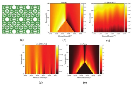
Figure 14.
(a) twisted -bilayer borophene, Chemical dependent (b) Seebeck coefficient, (c) thermal conductivity, (d) electrical conductivity, and (e) thermoelectric effect [120].
4. Conclusions
Based on the above discussions, Moiré superlattices have been extensively explored for various material properties and application research, including superconductivity, ferromagnetism, antiferromagnetism, topological properties, quantum Hall effect, optoelectronic applications, and so on.
In the field of superconductivity, Moiré superlattices provide a new approach to studying superconducting materials and open up new avenues for superconducting applications. The mechanisms of superconductivity, including critical currents and temperature ranges, need to be further understood. The role of electron–electron interactions, lattice effects, and other factors in promoting superconductivity also needs to be replicated. Moiré superlattices with ferromagnetic, antiferromagnetic, and topological properties also provide new platforms for the study of these materials. The stability of these magnetic behaviors is a key point that cannot be ignored. It is necessary to understand the relationship between twist angles, topological properties, and potential applications, offering the possibility of creating topologically protected states for various electronic and quantum applications. The study of the quantum Hall effect can also be conducted through Moiré superlattices, which is of great significance for developing new electronic devices.
In addition, Moiré superlattices have also been applied in the field of optoelectronics, such as photodetectors, solar cells, opto-control devices, etc. The realization of these applications requires in-depth research on the optoelectronic properties and performance of Moiré superlattices, as well as the development of efficient and controllable preparation methods.
Despite the progress that has been made in various fields using Moiré superlattices, there are still many unresolved issues and challenges, such as how to precisely control the structure and properties of Moiré superlattices, how to improve their preparation efficiency and scalability, and so on. With the continuous advancement of technology and methods, research and applications of Moiré superlattices are expected to continue to develop and provide new solutions for scientific and engineering problems in various fields.
Author Contributions
Content and design: M.S.; Writing of manuscript: J.S., S.W. and S.C.; Original writing: J.S.; All authors have read and agreed to the published version of the manuscript.
Funding
This work was supported by the National Science Foundation of China (12374181,11874407, 91436102, and 11374353) and the Fundamental Research Funds for the Central Universities (06500067).
Conflicts of Interest
The authors declare no conflict of interest.
References
- Novoselov, K.S.; Geim, A.K.; Morozov, S.V.; Jiang, D.; Zhang, Y.; Dubonos, S.V.; Grigorieva, I.V.; Firsov, A.A. Electric field effect in atomically thin carbon films. Science 2004, 306, 666–669. [Google Scholar] [CrossRef] [PubMed]
- Lemme, M.C.; Akinwande, D.; Huyghebaert, C.; Stampfer, C. 2D materials for future heterogeneous electronics. Nat. Commun. 2022, 13, 1392. [Google Scholar] [CrossRef]
- Choi, S.H.; Yun, S.J.; Won, Y.S.; Oh, C.S.; Kim, S.M.; Kim, K.K.; Lee, Y.H. Large-scale synthesis of graphene and other 2D materials towards industrialization. Nat. Commun. 2022, 13, 1484. [Google Scholar] [CrossRef] [PubMed]
- Bao, C.; Tang, P.; Sun, D.; Zhou, S. Light-induced emergent phenomena in 2D materials and topological materials. Nat. Rev. Phys. 2022, 4, 33–48. [Google Scholar] [CrossRef]
- Geim, A.K.; Grigorieva, I.V. Van der Waals heterostructures. Nature 2013, 499, 419–425. [Google Scholar] [CrossRef]
- Novoselov, K.S.; Mishchenko, A.; Carvalho, A.; Neto, A.H.C. 2D materials and van der Waals heterostructures. Science 2016, 353, aac9439. [Google Scholar] [CrossRef] [PubMed]
- Liu, Y.; Weiss, N.O.; Duan, X.; Cheng, H.-C.; Huang, Y.; Duan, X. Van der Waals heterostructures and devices. Nat. Rev. Mater. 2016, 1, 16042. [Google Scholar] [CrossRef]
- Li, W.; Yang, Z.; Sun, M.; Dong, J. Interlayer interactions in transition metal dichalcogenides heterostructures. Rev. Phys. 2022, 9, 100077. [Google Scholar] [CrossRef]
- Wang, Q.H.; Bedoya-Pinto, A.; Blei, M.; Dismukes, A.H.; Hamo, A.; Jenkins, S.; Koperski, M.; Liu, Y.; Sun, Q.-C.; Telford, E.J. The magnetic genome of two-dimensional van der Waals materials. ACS Nano 2022, 16, 6960. [Google Scholar] [CrossRef]
- Wu, Y.; Duan, J.; Ma, W.; Ou, Q.; Li, P.; Alonso-González, P.; Caldwell, J.D.; Bao, Q. Manipulating polaritons at the extreme scale in van der Waals materials. Nat. Rev. Phys. 2022, 4, 578–594. [Google Scholar] [CrossRef]
- Healey, A.; Scholten, S.; Yang, T.; Scott, J.; Abrahams, G.; Robertson, I.; Hou, X.; Guo, Y.; Rahman, S.; Lu, Y. Quantum microscopy with van der Waals heterostructures. Nat. Phys. 2023, 19, 87–91. [Google Scholar] [CrossRef]
- Castellanos-Gomez, A.; Duan, X.; Fei, Z.; Gutierrez, H.R.; Huang, Y.; Huang, X.; Quereda, J.; Qian, Q.; Sutter, E.; Sutter, P. Van der Waals heterostructures. Nat. Rev. Methods Primers 2022, 2, 58. [Google Scholar] [CrossRef]
- Wang, Q.H.; Kalantar-Zadeh, K.; Kis, A.; Coleman, J.N.; Strano, M.S. Electronics and optoelectronics of two-dimensional transition metal dichalcogenides. Nat. Nanotechnol. 2012, 7, 699–712. [Google Scholar] [CrossRef] [PubMed]
- Low, J.; Yu, J.; Jaroniec, M.; Wageh, S.; Al-Ghamdi, A.A. Heterojunction photocatalysts. Adv. Mater. 2017, 29, 1601694. [Google Scholar] [CrossRef]
- Li, X.; Shen, R.; Ma, S.; Chen, X.; Xie, J. Graphene-based heterojunction photocatalysts. Appl. Surf. Sci. 2018, 430, 53–107. [Google Scholar] [CrossRef]
- Dean, C.R.; Wang, L.; Maher, P.; Forsythe, C.; Ghahari, F.; Gao, Y.; Katoch, J.; Ishigami, M.; Moon, P.; Koshino, M.; et al. Hofstadter’s butterfly and the fractal quantum Hall effect in moiré superlattices. Nature 2013, 497, 598–602. [Google Scholar] [CrossRef]
- Zhang, Z.; Chen, P.; Duan, X.; Zang, K.; Luo, J.; Duan, X. Robust epitaxial growth of two-dimensional heterostructures, multiheterostructures, and superlattices. Science 2017, 357, 788–792. [Google Scholar] [CrossRef]
- Nam, N.N.T.; Koshino, M. Lattice relaxation and energy band modulation in twisted bilayer graphene. Phys. Rev. B 2017, 96, 075311. [Google Scholar] [CrossRef]
- Dai, Z.; Hu, G.; Si, G.; Ou, Q.; Zhang, Q.; Balendhran, S.; Rahman, F.; Zhang, B.Y.; Ou, J.Z.; Li, G.; et al. Edge-oriented and steerable hyperbolic polaritons in anisotropic van der Waals nanocavities. Nat. Commun. 2020, 11, 6086. [Google Scholar] [CrossRef]
- Du, L.; Molas, M.R.; Huang, Z.; Zhang, G.; Wang, F.; Sun, Z. Moiré photonics and optoelectronics. Science 2023, 379, eadg0014. [Google Scholar] [CrossRef]
- Schmidt, H.; Rode, J.C.; Smirnov, D.; Haug, R.J. Superlattice structures in twisted bilayers of folded graphene. Nat. Commun. 2014, 5, 5742. [Google Scholar] [CrossRef]
- Wang, J.; Mu, X.; Wang, L.; Sun, M. Properties and applications of new superlattice: Twisted bilayer graphene. Mater. Today Phys. 2019, 9, 100099. [Google Scholar] [CrossRef]
- Wang, D.; Chen, G.; Li, C.; Cheng, M.; Yang, W.; Wu, S.; Xie, G.; Zhang, J.; Zhao, J.; Lu, X.; et al. Thermally induced graphene rotation on hexagonal boron nitride. Phys. Rev. Lett. 2016, 116, 126101. [Google Scholar] [CrossRef] [PubMed]
- Yang, X.; Zhang, B. Heterostrain and temperature-tuned twist between graphene/h-BN bilayers. Sci. Rep. 2023, 13, 4364. [Google Scholar] [CrossRef] [PubMed]
- Li, G.; Luican, A.; Santos, J.M.B.L.D.; Neto, A.H.C.; Reina, A.; Kong, J.; Andrei, E.Y. Observation of Van Hove singularities in twisted graphene layers. Nat. Phys. 2010, 6, 109–113. [Google Scholar] [CrossRef]
- Ciepielewski, A.S.; Tworzydło, J.; Hyart, T.; Lau, A. Transport signatures of Van Hove singularities in mesoscopic twisted bilayer graphene. Phys. Rev. Res. 2022, 4, 043145. [Google Scholar] [CrossRef]
- Sanchez, D.S.; Cochran, T.A.; Belopolski, I.; Cheng, Z.-J.; Yang, X.P.; Liu, Y.; Hou, T.; Xu, X.; Manna, K.; Shekhar, C. Tunable topologically driven Fermi arc van Hove singularities. Nat. Phys. 2023, 19, 682–688. [Google Scholar] [CrossRef]
- Dean, C.R.; Young, A.F.; Meric, I.; Lee, C.; Wang, L.; Sorgenfrei, S.; Watanabe, K.; Taniguchi, T.; Kim, P.; Shepard, K.L.; et al. Boron nitride substrates for high-quality graphene electronics. Nat. Nanotechnol. 2010, 5, 722–726. [Google Scholar] [CrossRef]
- Xue, J.; Sanchez-Yamagishi, J.; Bulmash, D.; Jacquod, P.; Deshpande, A.; Watanabe, K.; Taniguchi, T.; Jarillo-Herrero, P.; LeRoy, B.J. Scanning tunnelling microscopy and spectroscopy of ultra-flat graphene on hexagonal boron nitride. Nat. Mater. 2011, 10, 282–285. [Google Scholar] [CrossRef]
- Giovannetti, G.; Khomyakov, P.A.; Brocks, G.; Kelly, P.J.; van den Brink, J. Substrate-induced band gap in graphene on hexagonal boron nitride: Ab initio density functional calculations. Phys. Rev. B 2007, 76, 073103. [Google Scholar] [CrossRef]
- Amet, F.; Williams, J.R.; Watanabe, K.; Taniguchi, T.; Goldhaber-Gordon, D. Insulating behavior at the neutrality point in single-layer graphene. Phys. Rev. Lett. 2013, 110, 216601. [Google Scholar] [CrossRef] [PubMed]
- Gorbachev, R.V.; Song, J.C.W.; Yu, G.L.; Kretinin, A.V.; Withers, F.; Cao, Y.; Mishchenko, A.; Grigorieva, I.V.; Novoselov, K.S.; Levitov, L.S.; et al. Detecting topological currents in graphene superlattices. Science 2014, 346, 448–451. [Google Scholar] [CrossRef] [PubMed]
- Hunt, B.; Sanchez-Yamagishi, J.D.; Young, A.F.; Yankowitz, M.; LeRoy, B.J.; Watanabe, K.; Taniguchi, T.; Moon, P.; Koshino, M.; Jarillo-Herrero, P.; et al. Massive Dirac fermions and Hofstadter butterfly in a van der Waals heterostructure. Science 2013, 340, 1427–1430. [Google Scholar] [CrossRef] [PubMed]
- Ponomarenko, L.A.; Gorbachev, R.V.; Yu, G.L.; Elias, D.C.; Jalil, R.; Patel, A.A.; Mishchenko, A.; Mayorov, A.S.; Woods, C.R.; Wallbank, J.R.; et al. Cloning of Dirac fermions in graphene superlattices. Nature 2013, 497, 594–597. [Google Scholar] [CrossRef] [PubMed]
- Alden, J.S.; Tsen, A.W.; Huang, P.Y.; Hovden, R.; Brown, L.; Park, J.; Muller, D.A.; McEuen, P.L. Strain solitons and topological defects in bilayer graphene. Proc. Natl. Acad. Sci. USA 2013, 110, 11256–11260. [Google Scholar] [CrossRef]
- San-Jose, P.; Gorbachev, R.V.; Geim, A.K.; Novoselov, K.S.; Guinea, F. Stacking boundaries and transport in bilayer graphene. Nano Lett. 2014, 14, 2052–2057. [Google Scholar] [CrossRef]
- Gargiulo, F.; Yazyev, O.V. Structural and electronic transformation in low-angle twisted bilayer graphene. 2D Mater. 2018, 5, 015019. [Google Scholar] [CrossRef]
- Wijk, M.M.V.; Schuring, A.; Katsnelson, M.I.; Fasolino, A. Relaxation of moiré patterns for slightly misaligned identical lattices: Graphene on graphite. 2D Mater. 2015, 2, 034010. [Google Scholar] [CrossRef]
- Wang, E.; Lu, X.; Ding, S.; Yao, W.; Yan, M.; Wan, G.; Deng, K.; Wang, S.; Chen, G.; Ma, L.; et al. Gaps induced by inversion symmetry breaking and second-generation Dirac cones in graphene/hexagonal boron nitride. Nat. Phys. 2016, 12, 1111–1115. [Google Scholar] [CrossRef]
- Smeyers, R.; Milošević, M.V.; Covaci, L. Strong gate-tunability of flat bands in bilayer graphene due to moiré encapsulation between hBN monolayers. Nanoscale 2023, 15, 4561–4569. [Google Scholar] [CrossRef]
- Lin, X.; Zhu, H.; Ni, J. High pressure induced secondary and tertiary gaps in relaxed graphene on hexagonal boron nitride. Phys. Rev. B 2022, 105, 075424. [Google Scholar] [CrossRef]
- Vu, N.H.; Le, H.V.; Phan, T.B.; Thoai, N.; Nguyen, T.T.; Le, H.M.; Kawazoe, Y.; Cao, T.M. Emergence of different replica Dirac cones and intra-and intervalley scatterings in short-wavelength graphene superlattices modulated by an atomic-scale sharp potential. J. Phys. Chem. C 2022, 126, 15415–15423. [Google Scholar] [CrossRef]
- Shaffer, D.; Wang, J.; Santos, L.H. Unconventional self-similar Hofstadter superconductivity from repulsive interactions. Nat. Commun. 2022, 13, 7785. [Google Scholar] [CrossRef] [PubMed]
- Adak, P.C.; Sinha, S.; Giri, D.; Mukherjee, D.K.; Chandan; Sangani, L.D.V.; Layek, S.; Mukherjee, A.; Watanabe, K.; Taniguchi, T.; et al. Perpendicular electric field drives Chern transitions and layer polarization changes in Hofstadter bands. Nat. Commun. 2022, 13, 7781. [Google Scholar] [CrossRef] [PubMed]
- Bistritzer, R.; MacDonald, A.H. Moiré bands in twisted double-layer graphene. Proc. Natl. Acad. Sci. USA 2011, 108, 12233–12237. [Google Scholar] [CrossRef]
- Cao, Y.; Fatemi, V.; Fang, S.; Watanabe, K.; Taniguchi, T.; Kaxiras, E.; Jarillo-Herrero, P. Unconventional superconductivity in magic-angle graphene superlattices. Nature 2018, 556, 43–50. [Google Scholar] [CrossRef]
- Cao, Y.; Fatemi, V.; Demir, A.; Fang, S.; Tomarken, S.L.; Luo, J.Y.; Sanchez-Yamagishi, J.D.; Watanabe, K.; Taniguchi, T.; Kaxiras, E.; et al. Correlated insulator behaviour at half-filling in magic-angle graphene superlattices. Nature 2018, 556, 80–84. [Google Scholar] [CrossRef]
- Utama, M.I.B.; Koch, R.J.; Lee, K.; Leconte, N.; Li, H.; Zhao, S.; Jiang, L.; Zhu, J.; Watanabe, K.; Taniguchi, T.; et al. Visualization of the flat electronic band in twisted bilayer graphene near the magic angle twist. Nat. Phys. 2021, 17, 184–188. [Google Scholar] [CrossRef]
- Lisi, S.; Lu, X.; Benschop, T.; de Jong, T.A.; Stepanov, P.; Duran, J.R.; Margot, F.; Cucchi, I.; Cappelli, E.; Hunter, A.; et al. Observation of flat bands in twisted bilayer graphene. Nat. Phys. 2021, 17, 189–193. [Google Scholar] [CrossRef]
- Hyart, T.; Ojajärvi, R.; Heikkilä, T. Two topologically distinct Dirac-line semimetal phases and topological phase transitions in rhombohedrally stacked honeycomb lattices. J. Low Temp. Phys. 2018, 191, 35–48. [Google Scholar] [CrossRef]
- Shashkin, A.; Dolgopolov, V.; Clark, J.; Shaginyan, V.; Zverev, M.; Khodel, V. Merging of Landau Levels in a Strongly Interacting Two-Dimensional Electron System in Silicon. Phys. Rev. Lett. 2014, 112, 186402. [Google Scholar] [CrossRef] [PubMed]
- Kauppila, V.; Aikebaier, F.; Heikkilä, T. Flat-band superconductivity in strained Dirac materials. Phys. Rev. B 2016, 93, 214505. [Google Scholar] [CrossRef]
- Mikitik, G.; Sharlai, Y.V. Dirac points of electron energy spectrum, band-contact lines, and electron topological transitions of 3 ½ kind in three-dimensional metals. Phys. Rev. B 2014, 90, 155122. [Google Scholar] [CrossRef]
- Bednorz, J.G.; Müller, K.A. Possible highTc superconductivity in the Ba−La−Cu−O system. Z. Phys. B 1986, 64, 189–193. [Google Scholar] [CrossRef]
- Yankowitz, M.; Chen, S.; Polshyn, H.; Zhang, Y.; Watanabe, K.; Taniguchi, T.; Graf, D.; Young, A.F.; Dean, C.R. Tuning superconductivity in twisted bilayer graphene. Science 2019, 363, 1059–1064. [Google Scholar] [CrossRef] [PubMed]
- Cao, Y.; Park, J.M.; Watanabe, K.; Taniguchi, T.; Jarillo-Herrero, P. Pauli-limit violation and re-entrant superconductivity in moiré graphene. Nature 2021, 595, 526–531. [Google Scholar] [CrossRef]
- Park, J.M.; Cao, Y.; Xia, L.-Q.; Sun, S.; Watanabe, K.; Taniguchi, T.; Jarillo-Herrero, P. Robust superconductivity in magic-angle multilayer graphene family. Nat. Mater. 2022, 21, 877–883. [Google Scholar] [CrossRef]
- Arora, H.S.; Polski, R.; Zhang, Y.; Thomson, A.; Choi, Y.; Kim, H.; Lin, Z.; Wilson, I.Z.; Xu, X.; Chu, J.-H.; et al. Superconductivity in metallic twisted bilayer graphene stabilized by WSe2. Nature 2020, 583, 379–384. [Google Scholar] [CrossRef]
- Chen, G.; Sharpe, A.L.; Gallagher, P.; Rosen, I.T.; Fox, E.J.; Jiang, L.; Lyu, B.; Li, H.; Watanabe, K.; Taniguchi, T.; et al. Signatures of tunable superconductivity in a trilayer graphene moiré superlattice. Nature 2019, 572, 215–219. [Google Scholar] [CrossRef]
- Tsui, D.C.; Stormer, H.L.; Gossard, A.C. Two-dimensional magnetotransport in the extreme quantum limit. Phys. Rev. Lett. 1982, 48, 1559. [Google Scholar] [CrossRef]
- Sanchez-Yamagishi, J.D.; Luo, J.Y.; Young, A.F.; Hunt, B.M.; Watanabe, K.; Taniguchi, T.; Ashoori, R.C.; Jarillo-Herrero, P. Helical edge states and fractional quantum Hall effect in a graphene electron–hole bilayer. Nature nanotechnology. Nat. Nanotechnol. 2017, 12, 118–122. [Google Scholar] [CrossRef] [PubMed]
- Lindner, N.H.; Berg, E.; Refael, G.; Stern, A. Fractionalizing majorana fermions: Non-abelian statistics on the edges of abelian quantum hall states. Phys. Rev. X 2012, 2, 041002. [Google Scholar] [CrossRef]
- Clarke, D.J.; Alicea, J.; Shtengel, K. Exotic non-Abelian anyons from conventional fractional quantum Hall states. Nat. Commun. 2013, 4, 1348. [Google Scholar] [CrossRef] [PubMed]
- Cheng, M. Superconducting proximity effect on the edge of fractional topological insulators. Phys. Rev. B 2012, 86, 195126. [Google Scholar] [CrossRef]
- Claassen, M.; Xian, L.; Kennes, D.M.; Rubio, A. Ultra-strong spin–orbit coupling and topological moiré engineering in twisted ZrS2 bilayers. Nat. Commun. 2022, 13, 4915. [Google Scholar] [CrossRef]
- Kang, J.; Vafek, O. Strong coupling phases of partially filled twisted bilayer graphene narrow bands. Phys. Rev. Lett. 2019, 122, 246401. [Google Scholar] [CrossRef] [PubMed]
- Xie, M.; MacDonald, A.H. Nature of the correlated insulator states in twisted bilayer graphene. Phys. Rev. Lett. 2020, 124, 097601. [Google Scholar] [CrossRef] [PubMed]
- Ochi, M.; Koshino, M.; Kuroki, K. Possible correlated insulating states in magic-angle twisted bilayer graphene under strongly competing interactions. Phys. Rev. B 2018, 98, 081102. [Google Scholar] [CrossRef]
- Thomson, A.; Chatterjee, S.; Sachdev, S.; Scheurer, M.S. Triangular antiferromagnetism on the honeycomb lattice of twisted bilayer graphene. Phys. Rev. B 2018, 98, 075109. [Google Scholar] [CrossRef]
- Venderbos, J.W.F.; Fernandes, R.M. Correlations and electronic order in a two-orbital honeycomb lattice model for twisted bilayer graphene. Phys. Rev. B 2018, 98, 245103. [Google Scholar] [CrossRef]
- Seo, K.; Kotov, V.N.; Uchoa, B. Ferromagnetic mott state in twisted graphene bilayers at the magic angle. Phys. Rev. Lett. 2019, 122, 246402. [Google Scholar] [CrossRef]
- Padhi, B.; Phillips, P.W. Pressure-induced metal-insulator transition in twisted bilayer graphene. Phys. Rev. B 2019, 99, 205141. [Google Scholar] [CrossRef]
- Sharpe, A.L.; Fox, E.J.; Barnard, A.W.; Finney, J.; Watanabe, K.; Taniguchi, T.; Kastner, M.A.; Goldhaber-Gordon, D. Emergent ferromagnetism near three-quarters filling in twisted bilayer graphene. Science 2019, 365, 605–608. [Google Scholar] [CrossRef] [PubMed]
- Chittari, B.L.; Chen, G.; Zhang, Y.; Wang, F.; Jung, J. Gate-tunable topological flat bands in trilayer graphene boron-nitride moiré superlattices. Phys. Rev. Lett. 2019, 122, 016401. [Google Scholar] [CrossRef]
- Zhang, Y.-H.; Mao, D.; Cao, Y.; Jarillo-Herrero, P.; Senthil, T. Nearly flat Chern bands in moiré superlattices. Phys. Rev. B 2019, 99, 075127. [Google Scholar] [CrossRef]
- Chen, G.; Jiang, L.; Wu, S.; Lyu, B.; Li, H.; Chittari, B.L.; Watanabe, K.; Taniguchi, T.; Shi, Z.; Jung, J. Evidence of a gate-tunable Mott insulator in a trilayer graphene moiré superlattice. Nat. Phys. 2019, 15, 237–241. [Google Scholar] [CrossRef]
- Hejazi, K.; Luo, Z.-X.; Balents, L. Noncollinear phases in moiré magnets. Proc. Natl. Acad. Sci. USA 2020, 117, 10721–10726. [Google Scholar] [CrossRef]
- Tong, Q.; Liu, F.; Xiao, J.; Yao, W. Skyrmions in the Moiré of van der Waals 2D Magnets. Nano Lett. 2018, 18, 7194–7199. [Google Scholar] [CrossRef] [PubMed]
- Chen, G.; Sharpe, A.L.; Fox, E.J.; Zhang, Y.-H.; Wang, S.; Jiang, L.; Lyu, B.; Li, H.; Watanabe, K.; Taniguchi, T.; et al. Tunable correlated Chern insulator and ferromagnetism in a moiré superlattice. Nature 2020, 579, 56–61. [Google Scholar] [CrossRef]
- Akram, M.; Erten, O. Skyrmions in twisted van der Waals magnets. Phys. Rev. B 2021, 103, L140406. [Google Scholar] [CrossRef]
- Xiao, F.; Chen, K.; Tong, Q. Magnetization textures in twisted bilayer Cr X3 (X = Br, I). Phys. Rev. Res. 2021, 3, 013027. [Google Scholar] [CrossRef]
- Xu, Y.; Ray, A.; Shao, Y.-T.; Jiang, S.; Lee, K.; Weber, D.; Goldberger, J.E.; Watanabe, K.; Taniguchi, T.; Muller, D.A.; et al. Coexisting ferromagnetic–antiferromagnetic state in twisted bilayer CrI3. Nat. Nanotechnol. 2022, 17, 143–147. [Google Scholar] [CrossRef] [PubMed]
- Wang, C.; Gao, Y.; Lv, H.; Xu, X.; Xiao, D. Stacking domain wall magnons in twisted van der Waals magnets. Phys. Rev. Lett. 2020, 125, 247201. [Google Scholar] [CrossRef]
- Koshino, M.; Oka, H. Topological invariants in two-dimensional quasicrystals. Phys. Rev. Res. 2022, 4, 013028. [Google Scholar] [CrossRef]
- Yerin, Y.; Varlamov, A.; Petrillo, C. Topological nature of the transition between the gap and the gapless superconducting states. Europhys. Lett. 2022, 138, 16005. [Google Scholar] [CrossRef]
- Tateishi, I.; Hirayama, M. Topological invariant and domain connectivity in moiré materials. Phys. Rev. B 2023, 107, 125308. [Google Scholar] [CrossRef]
- Mora, C.; Regnault, N.; Bernevig, B.A. Flatbands and perfect metal in trilayer moiré graphene. Phys. Rev. Lett. 2019, 123, 026402. [Google Scholar] [CrossRef] [PubMed]
- Ma, C.; Wang, Q.; Mills, S.; Chen, X.; Deng, B.; Yuan, S.; Li, C.; Watanabe, K.; Taniguchi, T.; Du, X. Moiré band topology in twisted bilayer graphene. Nano Lett. 2020, 20, 6076–6083. [Google Scholar] [CrossRef] [PubMed]
- Chen, S.; He, M.; Zhang, Y.-H.; Hsieh, V.; Fei, Z.; Watanabe, K.; Taniguchi, T.; Cobden, D.H.; Xu, X.; Dean, C.R.; et al. Electrically tunable correlated and topological states in twisted monolayer–bilayer graphene. Nat. Phys. 2021, 17, 374–380. [Google Scholar] [CrossRef]
- Xu, S.; Al Ezzi, M.M.; Balakrishnan, N.; Garcia-Ruiz, A.; Tsim, B.; Mullan, C.; Barrier, J.; Xin, N.; Piot, B.A.; Taniguchi, T.; et al. Tunable van Hove singularities and correlated states in twisted monolayer–bilayer graphene. Nat. Phys. 2021, 17, 619–626. [Google Scholar] [CrossRef]
- Polshyn, H.; Zhu, J.; Kumar, M.A.; Zhang, Y.; Yang, F.; Tschirhart, C.L.; Serlin, M.; Watanabe, K.; Taniguchi, T.; MacDonald, A.H.; et al. Electrical switching of magnetic order in an orbital Chern insulator. Nature 2020, 588, 66–70. [Google Scholar] [CrossRef] [PubMed]
- Choi, Y.; Kim, H.; Peng, Y.; Thomson, A.; Lewandowski, C.; Polski, R.; Zhang, Y.; Arora, H.S.; Watanabe, K.; Taniguchi, T.; et al. Correlation-driven topological phases in magic-angle twisted bilayer graphene. Nature 2021, 589, 536–541. [Google Scholar] [CrossRef] [PubMed]
- Nuckolls, K.P.; Oh, M.; Wong, D.; Lian, B.; Watanabe, K.; Taniguchi, T.; Bernevig, B.A.; Yazdani, A. Strongly correlated Chern insulators in magic-angle twisted bilayer graphene. Nature 2020, 588, 610–615. [Google Scholar] [CrossRef]
- Li, S.-Y.; Wang, Z.; Xue, Y.; Wang, Y.; Zhang, S.; Liu, J.; Zhu, Z.; Watanabe, K.; Taniguchi, T.; Gao, H.-J.; et al. Imaging topological and correlated insulating states in twisted monolayer-bilayer graphene. Nat. Commun. 2022, 13, 4225. [Google Scholar] [CrossRef]
- Tong, Q.; Yu, H.; Zhu, Q.; Wang, Y.; Xu, X.; Yao, W. Topological mosaics in moiré superlattices of van der Waals heterobilayers. Nat. Phys. 2017, 13, 356–362. [Google Scholar] [CrossRef]
- Huang, S.; Kim, K.; Efimkin, D.K.; Lovorn, T.; Taniguchi, T.; Watanabe, K.; MacDonald, A.H.; Tutuc, E.; LeRoy, B.J. Topologically protected helical states in minimally twisted bilayer graphene. Phys. Rev. Lett. 2018, 121, 037702. [Google Scholar] [CrossRef] [PubMed]
- Sunku, S.S.; Halbertal, D.; Stauber, T.; Chen, S.; McLeod, A.S.; Rikhter, A.; Berkowitz, M.E.; Lo, C.F.B.; Gonzalez-Acevedo, D.E.; Hone, J.C.; et al. Hyperbolic enhancement of photocurrent patterns in minimally twisted bilayer graphene. Nat. Commun. 2021, 12, 1641. [Google Scholar] [CrossRef]
- Kerelsky, A.; McGilly, L.J.; Kennes, D.M.; Xian, L.; Yankowitz, M.; Chen, S.; Watanabe, K.; Taniguchi, T.; Hone, J.; Dean, C.; et al. Maximized electron interactions at the magic angle in twisted bilayer graphene. Nature 2019, 572, 95–100. [Google Scholar] [CrossRef]
- Xie, Y.; Lian, B.; Jäck, B.; Liu, X.; Chiu, C.-L.; Watanabe, K.; Taniguchi, T.; Bernevig, B.A.; Yazdani, A. Spectroscopic signatures of many-body correlations in magic-angle twisted bilayer graphene. Nature 2019, 572, 101–105. [Google Scholar] [CrossRef]
- Jiang, Y.; Lai, X.; Watanabe, K.; Taniguchi, T.; Haule, K.; Mao, J.; Andrei, E.Y. Charge order and broken rotational symmetry in magic-angle twisted bilayer graphene. Nature 2019, 573, 91–95. [Google Scholar] [CrossRef]
- Choi, Y.; Kemmer, J.; Peng, Y.; Thomson, A.; Arora, H.; Polski, R.; Zhang, Y.; Ren, H.; Alicea, J.; Refael, G.; et al. Electronic correlations in twisted bilayer graphene near the magic angle. Nat. Phys. 2019, 15, 1174–1180. [Google Scholar] [CrossRef]
- Ju, L.; Shi, Z.; Nair, N.; Lv, Y.; Jin, C.; Velasco, J.; Ojeda-Aristizabal, C.; Bechtel, H.A.; Martin, M.C.; Zettl, A.; et al. Topological valley transport at bilayer graphene domain walls. Nature 2015, 520, 650–655. [Google Scholar] [CrossRef] [PubMed]
- Jiang, B.-Y.; Ni, G.-X.; Addison, Z.; Shi, J.K.; Liu, X.; Zhao, S.Y.F.; Kim, P.; Mele, E.J.; Basov, D.N.; Fogler, M.M. Plasmon reflections by topological electronic boundaries in bilayer graphene. Nano Lett. 2017, 17, 7080–7085. [Google Scholar] [CrossRef] [PubMed]
- Sunku, S.S.; Ni, G.X.; Jiang, B.Y.; Yoo, H.; Sternbach, A.; McLeod, A.S.; Stauber, T.; Xiong, L.; Taniguchi, T.; Watanabe, K.; et al. Photonic crystals for nano-light in moiré graphene superlattices. Science 2018, 362, 1153–1156. [Google Scholar] [CrossRef] [PubMed]
- Yin, L.-J.; Jiang, H.; Qiao, J.-B.; He, L. Direct imaging of topological edge states at a bilayer graphene domain wall. Nat. Commun. 2016, 7, 11760. [Google Scholar] [CrossRef]
- Xu, X.; Gabor, N.M.; Alden, J.S.; van der Zande, A.M.; McEuen, P.L. Photo-thermoelectric effect at a graphene interface junction. Nano Lett. 2010, 10, 562–566. [Google Scholar] [CrossRef]
- Gabor, N.M.; Song, J.C.W.; Ma, Q.; Nair, N.L.; Taychatanapat, T.; Watanabe, K.; Taniguchi, T.; Levitov, L.S.; Jarillo-Herrero, P. Hot carrier–assisted intrinsic photoresponse in graphene. Science 2011, 334, 648–652. [Google Scholar] [CrossRef]
- Song, J.C.W.; Rudner, M.S.; Marcus, C.M.; Levitov, L.S. Hot carrier transport and photocurrent response in graphene. Nano Lett. 2011, 11, 4688–4692. [Google Scholar] [CrossRef]
- Song, J.C.W.; Levitov, L.S. Shockley-Ramo theorem and long-range photocurrent response in gapless materials. Phys. Rev. B 2014, 90, 075415. [Google Scholar] [CrossRef]
- Lu, X.; Stepanov, P.; Yang, W.; Xie, M.; Aamir, M.A.; Das, I.; Urgell, C.; Watanabe, K.; Taniguchi, T.; Zhang, G.; et al. Superconductors, orbital magnets and correlated states in magic-angle bilayer graphene. Nature 2019, 574, 653–657. [Google Scholar] [CrossRef]
- de Vries, F.K.; Portolés, E.; Zheng, G.; Taniguchi, T.; Watanabe, K.; Ihn, T.; Ensslin, K.; Rickhaus, P. Gate-defined Josephson junctions in magic-angle twisted bilayer graphene. Nat. Nanotechnol. 2021, 16, 760–763. [Google Scholar] [CrossRef]
- Rodan-Legrain, D.; Cao, Y.; Park, J.M.; de la Barrera, S.C.; Randeria, M.T.; Watanabe, K.; Taniguchi, T.; Jarillo-Herrero, P. Highly tunable junctions and non-local Josephson effect in magic-angle graphene tunnelling devices. Nat. Nanotechnol. 2021, 16, 769–775. [Google Scholar] [CrossRef] [PubMed]
- Diez-Merida, J.; Díez-Carlón, A.; Yang, S.; Xie, Y.-M.; Gao, X.-J.; Watanabe, K.; Taniguchi, T.; Lu, X.; Law, K.T.; Efetov, D.K. Magnetic Josephson junctions and superconducting diodes in magic angle twisted bilayer graphene. arXiv 2021, arXiv:2110.01067. [Google Scholar]
- Portolés, E.; Iwakiri, S.; Zheng, G.; Rickhaus, P.; Taniguchi, T.; Watanabe, K.; Ihn, T.; Ensslin, K.; de Vries, F.K. A tunable monolithic SQUID in twisted bilayer graphene. Nat. Nanotechnol. 2022, 17, 1159–1164. [Google Scholar] [CrossRef] [PubMed]
- Qin, F.; Shi, W.; Ideue, T.; Yoshida, M.; Zak, A.; Tenne, R.; Kikitsu, T.; Inoue, D.; Hashizume, D.; Iwasa, Y. Superconductivity in a chiral nanotube. Nat. Commun. 2017, 8, 14465. [Google Scholar] [CrossRef]
- Dong, J.; Zhang, L.; Dai, X.; Ding, F. The epitaxy of 2D materials growth. Nat. Commun. 2020, 11, 5862. [Google Scholar] [CrossRef] [PubMed]
- Xie, L.; Wang, L.; Zhao, W.; Liu, S.; Huang, W.; Zhao, Q. WS2 moiré superlattices derived from mechanical flexibility for hydrogen evolution reaction. Nat. Commun. 2021, 12, 5070. [Google Scholar] [CrossRef] [PubMed]
- Kibsgaard, J.; Jaramillo, T.F.; Besenbacher, F. Building an appropriate active-site motif into a hydrogen-evolution catalyst with thiomolybdate [Mo3S13]2− clusters. Nat. Chem. 2014, 6, 248–253. [Google Scholar] [CrossRef]
- Gauthier, J.A.; King, L.A.; Stults, F.T.; Flores, R.A.; Kibsgaard, J.; Regmi, Y.N.; Chan, K.; Jaramillo, T.F. Transition metal arsenide catalysts for the hydrogen evolution reaction. J. Phys. Chem. C 2019, 123, 24007–24012. [Google Scholar] [CrossRef]
- Song, J.; Cao, Y.; Dong, J.; Sun, M. Superior Thermoelectric Properties of Twist-Angle Superlattice Borophene Induced by Interlayer Electrons Transport. Small 2023, 19, 2301348. [Google Scholar] [CrossRef]


Disclaimer/Publisher’s Note: The statements, opinions and data contained in all publications are solely those of the individual author(s) and contributor(s) and not of MDPI and/or the editor(s). MDPI and/or the editor(s) disclaim responsibility for any injury to people or property resulting from any ideas, methods, instructions or products referred to in the content. |
© 2023 by the authors. Licensee MDPI, Basel, Switzerland. This article is an open access article distributed under the terms and conditions of the Creative Commons Attribution (CC BY) license (https://creativecommons.org/licenses/by/4.0/).