Article

Cluster Formation Effect of Water on Pristine and Defective MoS2 Monolayers

Institut für Chemie und Biochemie, Freie Universität Berlin, Arnimallee 22, 14195 Berlin, Germany
*
Authors to whom correspondence should be addressed.
Nanomaterials 2023, 13(2), 229; https://doi.org/10.3390/nano13020229
Submission received: 30 November 2022 / Revised: 23 December 2022 / Accepted: 27 December 2022 / Published: 4 January 2023
(This article belongs to the Special Issue Graphene and Related 2D Materials)

Abstract

:
The structure and electronic properties of the molybdenum disulfide (MoS2) monolayer upon water cluster adsorption are studied using density functional theory and the optical properties are further analyzed with the Bethe–Salpeter equation (BSE). Our results reveal that the water clusters are electron acceptors, and the acceptor tendency tends to increase with the size of the water cluster. The electronic band gap of both pristine and defective MoS2 is rather insensitive to water cluster adsorbates, as all the clusters are weakly bound to the MoS2 surface. However, our calculations on the BSE level show that the adsorption of the water cluster can dramatically redshift the optical absorption for both pristine and defective MoS2 monolayers. The binding energy of the excitons of MoS2 is greatly enhanced with the increasing size of the water cluster and finally converges to a value of approximately 1.16 eV and 1.09 eV for the pristine and defective MoS2 monolayers, respectively. This illustrates that the presence of the water cluster could localize the excitons of MoS2, thereby greatly enhance the excitonic binding energy.

Graphical Abstract

1. Introduction

Recently, layered transition metal dichalcogenides (TMDs) have gained great attention due to their unusual electronic and optical properties, including sizable band gap, strong photoluminescence, excitonic effect, valley-specific circular dichroism, and so on [1,2,3,4,5,6,7,8]. For instance, while the bulk MoS2 is an indirect band gap semiconductor, monolayer MoS2 is a direct band gap semiconductor. Importantly, the exciton in the MoS2 monolayer is strongly bound because of the reduced dimensionality. The presence of intrinsic structural defects in TMDs [9,10,11], which is inevitable in the experiments, provides even more possibility to tune the reactivity and transport properties and create new functionalities. For example, NO molecules can chemically adsorb on the sulfur (S) defects of the MoS2 monolayer [12,13,14], indicating the high sensitivity towards NO molecules and the great potential of TMDs as gas sensors. These suggest that the layered TMDs, in particular MoS2, are promising candidates for graphene replacement with various application possibilities.
In reality, the humidity, i.e., the effect of adsorption of water, plays an important role in countless applications and technological processes, since water is present in the environment of almost any device. Examples include field-effect transistors [15], gas sensors [16,17], and electronic devices [18]. In addition, various water clusters (H2O)n can form via intermolecular hydrogen bonds on the surface of a solid depending on the environmental conditions [19,20,21,22,23,24,25,26]. Therefore, the understanding of the properties of water/solid interface is very important for the development and improvement of various applications.
The great potential of the MoS2 monolayer and the importance of the water/solid interface call for a theoretical perspective on how the presence of water influences the electronic and optical properties of MoS2. A single water molecule was theoretically predicted to only weakly adsorb on the MoS2 surface compared with other inorganic molecules, and had no influence on the electronic band gap [12,13,27,28,29,30]. However, there is still a lack of theoretical understanding of the influence of a single water molecule on the optical and excitonic properties. More importantly, the effect of water clusters associated with hydrogen bonds on the electronic and optical properties of the MoS2 monolayer is still largely unexplored.
It is well known that the GW approximation combined with the Bethe–Salpeter equation based on DFT (DFT-GW-BSE) [31,32,33] can accurately model photoemission measurements and optical absorption. In this work, by employing this method, we analyze how the water cluster influences the electronic, optical and excitonic properties of both pristine and defective MoS2 monolayers. In this model, a water cluster consisting of up to five water molecules is considered to adsorb on a large supercell of the MoS2 monolayer.

2. Computational Details

All calculations except for the charge density difference are performed using GPAW code [34] based on the projector augmented wave method. To describe the exchange and correlation effects, including the dispersion interaction, we adopt the vdW-DF-CX functional [35] to obtain the structures upon water cluster adsorption. A cutoff energy of 500 eV for the plane-wave basis set and a Monkhorst–Pack k-point sampling of 6 × 6 × 1 are employed. The S defect is the main factor among the intrinsic structural defects in TMDs. Therefore, in order to ensure that the S defect density in our simulation models is in the same magnitude of experimental density (1013 cm−2) [9,36], one S defect is created in a (4 × 4) supercell of the MoS2 monolayer, corresponding to a defect density of 6.2 × 1013 cm−2. A vacuum space of more than 15 Å is chosen during geometry optimization to avoid undesired interactions between neighboring supercells in the perpendicular direction. The clusters containing up to five water molecules are considered to absorb on the MoS2 surface. All the structures are fully relaxed until the maximum force acting on each atom is less than 0.02 eV/Å and the energy change is less than 10−5 eV. Within this frame, we obtain a lattice constant of 3.18 Å and a Mo-S bond length of 2.41 Å for the pristine MoS2, which are in good agreement with experimental results [37] and previous simulations [38,39]. Using the optimized structures, the charge transfer between adsorbate and substrate is discussed by means of Bader analysis [40]. The charge density calculation is performed by means of the DFT method at the vdW-DF-CX level using the plane wave Vienna ab initio Simulation Package (VASP) code [41,42] and the same computational parameters as for the GPAW calculations.
The DFT-GW-BSE method is a three-step procedure to determine the electronic and optical properties of a solid. The first step is to obtain the Kohn–Sham energies and wave functions by DFT calculation. In the second step, the quasi-particle (QP) band structure energies are obtained by GW approximation. Finally, the BSE is solved to get the coupled electron–hole excitation energies and exciton wave functions. Motivated by the weak interaction between adsorbate and substrate and the high cost of GW calculation, we use an approximated method, DFT-appG0W0-BSE (one-shot G0W0: GW equations are not solved self-consistently), to perform the BSE calculation. In this method, the electron–hole interaction is approximated by applying the scissor operator to the DFT band structure of the adsorbate/substrate system according to the QP band gap of the substrate (as displayed in Figure 1), motivated by the negligible influence of the adsorbate on the electron–hole interaction in a certain range. To enable a more direct comparison with DFT-GW-BSE, we apply the DFT-G0W0-BSE and DFT-appG0W0-BSE methods to the case of a single H2O molecule on the pristine MoS2 unit cell. The corresponding results are displayed in Figure 2. It is clear that the optical absorption spectrum calculated by the DFT-appG0W0-BSE method is in good agreement with that by the DFT-G0W0-BSE method within 0.05 eV deviation.
After successfully applying the DFT-appG0W0-BSE method to describe the optical properties of a single H2O molecule on the pristine MoS2 unit cell, we extend our investigation to the optical properties of the water cluster on a (4 × 4) supercell. The DFT calculation is performed by the general gradient approximation along with the Perdew–Burke–Ernzerhof (PBE) exchange–correlation functional [43]. Our previous study [39] shows that for a (4 × 4) supercell, 10 Å vacuum with 50 eV G0W0 self-energy and 3 × 3 × 1 k-point sampling is sufficient to obtain the converged QP band gap by employing the 2D truncation. Therefore, the same parameters are applied to the G0W0 calculation of the pristine and defective MoS2. To obtain converged optical spectra, the 16 highest valence bands and the 32 lowest conduction bands are used as a basis to calculate excitonic contribution with a large k-point grid of 8 × 8 × 1. The spectrum is obtained by applying a Lorentzian broadening with a fullwidth half maximum of 0.05 eV.

3. Results

3.1. Configurations of (H2O)n on MoS2 Monolayers

We first investigate the adsorption of (H2O)n on both pristine and defective MoS2 surfaces by identifying the most stable adsorption structures. Various high-symmetry adsorption sites and adsorption orientations are considered; the most favorable configurations and corresponding results are presented in Figure 3 and Table 1, respectively. We discriminate between the adsorption energy of the whole cluster on MoS2 and the binding energy, which is referred to the isolated water molecules. The adsorption energy is calculated as
E a d = E t o t E M o S 2 E c l u s t e r
where E t o t represents the total energy of MoS2 with cluster adsorbed, E M o S 2 and E c l u s t e r are the energies of the MoS2 monolayer and the isolated cluster. The binding energy is determined using
E b i n d = E t o t E M o S 2 n E H 2 O
where E t o t , E M o S 2 , E H 2 O , and n are the total energy of MoS2 with the cluster adsorbed, the energy of the MoS2 monolayer, the energy of relaxed H2O molecule, and the number of H2O molecules in the cluster, respectively. As shown in Figure 3, for the pristine surface, the monomer H2O is preferably adsorbed at the hollow site, with two O-H bonds orienting towards the monolayer. In the case of the dimer, trimer, tetramer, and pentamer, water clusters prefer to form the linear, triangular, quadrilateral, and pentagonal shapes on the surface of MoS2, respectively. In particular, we observe that a ring trimer is more stable than an open structure on the MoS2 surface, which differs from that on the Pt(111) surface [44]. In addition, due to the cluster–surface interaction, these water clusters tend to lie on the pristine surface. Generally speaking, the shape and orientation of water clusters on the pristine MoS2 surface are almost identical to the gas-phase of water clusters [45,46,47,48]. As displayed in Table 1, the binding energy of water clusters on the pristine surface dramatically increases with the increasing size of the cluster as more hydrogen bonds form within the cluster. We also note that the hydrogen bonds in the cluster become stronger with the size of the water cluster, e.g., trimer: 0.23 eV, tetramer: 0.31 eV, and pentamer: 0.33 eV. This is because the angular strain becomes smaller in a large water cluster. In comparison with the adsorption energy, the binding energy has a larger negative value since it contains contributions from the intermolecular hydrogen bonding in addition to the cluster–surface interaction. Both binding and adsorption energies show that the water cluster binds stronger to the MoS2 surface than monomer water, indicating the tendency towards larger water clusters on the MoS2 surface. In general, the water clusters are weakly bound to the pristine MoS2 with a large separation bigger than 2.98 Å between them.
For the defective surface, we find that the monomer water adopts a vertical configuration with one O-H bond pointing towards the defect, which is in good agreement with the previous calculations [12]. When the dimer, trimer, tetramer, and pentamer adsorb on the defective MoS2 surface, the structure of the water clusters changes as influenced by hydrogen bonding and cluster–defect interactions. Therefore, one molecule of the water cluster is always adsorbed at the defect with a small separation. The adsorption energy of water clusters on the defective surface (in range of −0.21 eV to −0.54 eV) is slightly larger than that on the pristine surface (in range of −0.14 to −0.49 eV), implying that the defect is a center of adsorption. Although the adsorption energy and distance between the water cluster and MoS2 monolayer are greatly influenced by the presence of the defect, all these water clusters are only physisorbed on the defective MoS2.

3.2. Electronic Properties

Figure 4 and Table 1 display how the electron density rearranges upon the adsorption of the water clusters. The corresponding charge density difference is calculated by the formula Δ ρ = ρ t o t ρ M o S 2 ρ c l u s t e r , where ρ t o t , ρ M o S 2 and ρ c l u s t e r are the charge density of the MoS2 with adsorption, MoS2 monolayer, and isolated cluster, respectively. It is shown that for both pristine and defective MoS2, the oxygen atom in the water gains charge density, while the hydrogens lose charge density, resulting in a small number of electrons to be transferred from MoS2 to the water cluster. It also implies that the charge rearrangement between MoS2 and the water cluster depends on the orientation of the water molecule. For example, when a water dimer is adsorbed on the pristine surface, 0.022 e is transferred from the MoS2 to one water molecule (labeled as H2O(2) in Table 1); while 0.005 e is transferred to the MoS2 from the other water molecule (labeled as H2O(1) in Table 1). The charge rearrangement mainly occurs on the S atoms and partly on the Mo atoms of MoS2 around each absorption site. As the water cluster grows, the charge transfer between the water cluster and host tends to converge for both pristine and defective surfaces. Compared with the pristine surface, a larger charge transfer occurs between the water cluster and the defective MoS2, also reflected by their stronger adsorption as described above. As revealed by Table 1, up to 0.033 e is transferred from the defective MoS2 to the water cluster. The transferred electrons are mainly distributed in the water molecule adsorbed at the S defect (labeled as H2O(1)). This behavior arises from the presence of the unsaturated Mo atom on the surface, which leaves excess electrons at the S defect. We can conclude overall from this analysis that the water clusters acting as electron acceptors induce charge redistribution for both pristine and defective MoS2 hosts.
We next examine the band structure and DOS (see Supporting Information) of the water cluster adsorbing on both pristine and defective MoS2 surfaces. Since the DFT method always underestimates the band gap, the G0W0 calculation is performed for the pristine and defective MoS2. For the pristine MoS2 monolayer, our G0W0 band gap of 2.55 eV is slightly larger than our previous result of 2.49 eV, mainly due to the exclusion of spin–orbit interaction in the present work. We find that the spin–orbit splitting calculated by G0W0 is almost the same as vdW-DF-CX. Therefore, after including the spin–orbit splitting from the DFT method at the vdW-DF-CX level, the calculated band gap of 2.48 eV of the pristine MoS2 monolayer agrees well with the experimental values of approximately 2.5 eV [49]. The presence of an S defect on the MoS2 induces three localized states in the band gap: two unoccupied states around 1.58 eV and one occupied state around −0.42 eV (see Figure S1 in Supporting Information). In addition, the unoccupied states undergo a spin–orbit splitting of 0.05 eV at the K point, giving rise to a QP band gap of 1.95 eV. Concerning the adsorption of the water clusters, our DFT band structure and DOS calculation show that the molecular states are present deeply in the valence band and conduction band of MoS2 and hybrids with host states, implying that the band gap of MoS2 is insensitive towards perturbations by the water clusters. Thus, the G0W0 calculation will not be performed upon the adsorption of the water clusters.

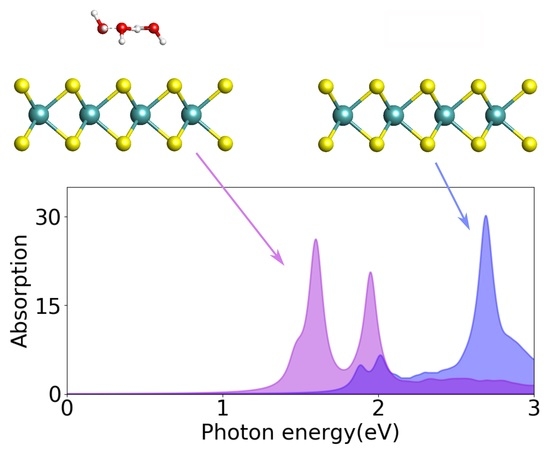
3.3. Optical and Excitonic Properties

We proceed to investigate the optical properties of (H2O)n/MoS2 by solving the BSE equations. Figure 5 depicts the optical absorption spectra with and without the adsorption of water clusters on the MoS2 monolayer, and the corresponding results are summarized in Table 2. The calculated optical band gap of 1.89 eV for the pristine MoS2 monolayer is in excellent agreement with the experimental value of approximately 1.9 eV [6,49]. As a result, the corresponding excitonic binding energy of 0.59 eV is obtained in this work. The sharp peaks A and B are located at 1.89 eV and 2.02 eV, respectively, associating with the direct transitions from the spin–orbit split valence band to the conduction bands at the K point in the Brillouin zone. The adsorption of the monomer water on the pristine MoS2 dramatically redshifts the absorption edge of the optical spectrum and induces an absorption shoulder at 1.64 eV, corresponding to a strongly bound exciton with 0.84 eV binding energy. It is well known that the excitons in 2D-TMDs are of the Wannier–Mott type and thus delocalized in space [50]. A localized exciton with strong electron–hole interaction is observed upon the adsorption of the water cluster. In addition, as the water cluster grows, the optical absorption peak is shifted to lower energy and the binding energy of excitons becomes larger, and both of them finally converge to a value of approximately 1.32 eV and 1.17 eV, respectively. This convergence indicates that the exciton binding energy may be insensitive to further growth of the water cluster. More interestingly, the optical absorption is greatly strengthened in the spectral range of 1.5–2.5 eV. The enhanced optical absorption is attributed to the charge transfer between the water cluster and host which depletes the n-type conductivity in MoS2 and further reduces the electrostatic screening [51,52].
In comparison with the pristine MoS2, the presence of an S defect greatly redshifts the first absorption peak to 1.32 eV with attenuated intensity. The excitonic binding energy with 0.63 eV is slightly stronger than that of the pristine MoS2. This is because the unsaturated Mo atom leaves excess electrons at the S defect, leading to the formation of the charged exciton. The adsorption of the water clusters on the defective surface also redshifts the optical absorption edge compared with that on the pristine MoS2, but the optical band gap converges to a smaller value of approximately 0.86 eV with the increasing size of the water cluster. Thus, the binding energy of the charged exciton converges to a value of approximately 1.09 eV with the increasing size of the water cluster. Although the first optical absorption peak is weakened by the adsorption of the water clusters, the optical absorption between 1.5 and 2.0 eV is greatly strengthened as similarly observed for the pristine MoS2 series. In conclusion, the optical absorption of both pristine and defective MoS2 can be redshifted and is further enhanced in the infrared region by water clusters adsorption.

4. Conclusions

In summary, by employing the DFT-appG0W0-BSE method, we explored how the electronic and optical properties of the MoS2 monolayer are affected by the adsorption of water clusters of different sizes. It was found that (1) the water clusters (H2O)n (n = 1–5) have weak interaction with both pristine and defective MoS2 monolayers, (2) no additional states are introduced in the gap region of both pristine and defective MoS2 by the adsorption of the water clusters; and (3) the presence of the water clusters can dramatically redshift the optical absorption for both pristine and defective MoS2 monolayers.

Supplementary Materials

The following supporting information can be downloaded at: https://www.mdpi.com/article/10.3390/nano13020229/s1, Figure S1: electronic band structure for the pristine and defective MoS2 monolayers; Figures S2 and S3: electronic band structure for (H2O)n (n = 1–5) on the pristine and defective MoS2 monolayers, respectively; Figure S4: total density of states and the projected density of states for (H2O)n (n = 1–5) on pristine and defective MoS2; optimized geometries considered in this work.

Author Contributions

Conceptualization, B.P. and K.W.; formal analysis, K.W.; funding acquisition, B.P. and K.W.; investigation, K.W.; resources, B.P. and K.W.; supervision, B.P.; validation, K.W.; visualization, K.W.; writing—original draft, K.W.; writing—review and editing, K.W. and B.P. All authors have read and agreed to the published version of the manuscript.

Funding

This research received no external funding. The publication of this article was funded by Freie Universität Berlin.

Institutional Review Board Statement

Not applicable.

Informed Consent Statement

Not applicable.

Data Availability Statement

Not applicable.

Acknowledgments

K.W. acknowledges the China Scholarship Council for the financial support. B.P. and K.W. thank Kirill Bolotin for the fruitful discussions. The computations were performed with resources provided by the North-German Supercomputing Alliance (HLRN) and computer facilities of the Freie Universitäte Berlin (ZEDAT).

Conflicts of Interest

The authors have no conflict to declare.

References

  1. Gusakova, J.; Wang, X.; Shiau, L.L.; Krivosheeva, A.; Shaposhnikov, V.; Borisenko, V.; Gusakov, V.; Tay, B.K. Electronic Properties of Bulk and Monolayer TMDs: Theoretical Study Within DFT Framework (GVJ-2e Method). Phys. Status Solidi A 2017, 214, 1700218. [Google Scholar] [CrossRef]
  2. Kylänpää, I.; Komsa, H.-P. Binding energies of exciton complexes in transition metal dichalcogenide monolayers and effect of dielectric environment. Phys. Rev. B 2015, 92, 205418. [Google Scholar] [CrossRef] [Green Version]
  3. Berghäuser, G.; Malic, E. Analytical approach to excitonic properties of MoS2. Phys. Rev. B 2014, 89, 125309. [Google Scholar] [CrossRef] [Green Version]
  4. Ramasubramaniam, A. Large excitonic effects in monolayers of molybdenum and tungsten dichalcogenides. Phys. Rev. B 2012, 86, 115409. [Google Scholar] [CrossRef] [Green Version]
  5. He, K.; Kumar, N.; Zhao, L.; Wang, Z.; Mak, K.F.; Zhao, H.; Shan, J. Tightly Bound Excitons in Monolayer WSe2. Phys. Rev. Lett. 2014, 113, 026803. [Google Scholar] [CrossRef] [PubMed] [Green Version]
  6. Mak, K.F.; Lee, C.; Hone, J.; Shan, J.; Heinz, T.F. Atomically Thin MoS2: A New Direct-Gap Semiconductor. Phys. Rev. Lett. 2010, 105, 136805. [Google Scholar] [CrossRef] [Green Version]
  7. Mak, K.F.; He, K.; Shan, J.; Heinz, T.F. Control of valley polarization in monolayer MoS2 by optical helicity. Nat. Nanotechnol. 2012, 7, 494–498. [Google Scholar] [CrossRef] [PubMed]
  8. Splendiani, A.; Sun, L.; Zhang, Y.; Li, T.; Kim, J.; Chim, C.-Y.; Galli, G.; Wang, F. Emerging Photoluminescence in Monolayer MoS2. Nano Lett. 2010, 10, 1271–1275. [Google Scholar] [CrossRef]
  9. Hong, J.; Hu, Z.; Probert, M.; Li, K.; Lv, D.; Yang, X.; Gu, L.; Mao, N.; Feng, Q.; Xie, L.; et al. Exploring atomic defects in molybdenum disulphide monolayers. Nat. Commun. 2015, 6, 6293. [Google Scholar] [CrossRef] [Green Version]
  10. Zhou, W.; Zou, X.; Najmaei, S.; Liu, Z.; Shi, Y.; Kong, J.; Lou, J.; Ajayan, P.M.; Yakobson, B.I.; Idrobo, J.-C. Intrinsic structural defects in monolayer molybdenum disulfide. Nano Lett. 2013, 13, 2615–2622. [Google Scholar] [CrossRef]
  11. Stampfer, B.; Zhang, F.; Illarionov, Y.Y.; Knobloch, T.; Wu, P.; Waltl, M.; Grill, A.; Appenzeller, J.; Grasser, T. Characterization of Single Defects in Ultrascaled MoS2 Field-Effect Transistors. ACS Nano 2018, 12, 5368–5375. [Google Scholar] [CrossRef] [PubMed]
  12. Li, H.; Huang, M.; Cao, G. Markedly different adsorption behaviors of gas molecules on defective monolayer MoS2: A first-principles study. Phys. Chem. Chem. Phys. 2016, 18, 15110–15117. [Google Scholar] [CrossRef] [PubMed]
  13. González, C.; Biel, B.; Dappe, Y.J. Adsorption of small inorganic molecules on a defective MoS2 monolayer. Phys. Chem. Chem. Phys. 2017, 19, 9485–9499. [Google Scholar] [CrossRef] [PubMed] [Green Version]
  14. Li, F.; Shi, C. NO-sensing performance of vacancy defective monolayer MoS2 predicted by density function theory. Appl. Surf. Sci. 2017, 434, 294–306. [Google Scholar] [CrossRef]
  15. Lowe, B.M.; Maekawa, Y.; Shibuta, Y.; Sakata, T.; Skylaris, C.-K.; Green, N.G. Dynamic behaviour of the silica-water-bio electrical double layer in the presence of a divalent electrolyte. Phys. Chem. Chem. Phys. 2017, 19, 2687–2701. [Google Scholar] [CrossRef] [Green Version]
  16. Kokabu, T.; Inoue, S.; Matsumura, Y. Effect of molecular coverage on the electric conductance of a multi-walled carbon nanotube thin film. Chem. Phys. Lett. 2016, 654, 9–12. [Google Scholar] [CrossRef]
  17. Kokabu, T.; Takashima, K.; Inoue, S.; Matsumura, Y.; Yamamoto, T. Transport phenomena of electrons at the carbon nanotube interface with molecular adsorption. J. Appl. Phys. 2017, 122, 015308. [Google Scholar] [CrossRef]
  18. Melios, C.; Giusca, C.E.; Panchal, V.; Kazakova, O. Water on graphene: Review of recent progress. 2D Mater. 2018, 5, 022001. [Google Scholar] [CrossRef] [Green Version]
  19. Thiel, P.A.; Madey, T.E. The interaction of water with solid surfaces: Fundamental aspects. Surf. Sci. Rep. 1987, 7, 211–385. [Google Scholar] [CrossRef]
  20. Henderson, M.A. The interaction of water with solid surfaces: Fundamental aspects revisited. Surf. Sci. Rep. 2002, 46, 1–308. [Google Scholar] [CrossRef]
  21. Hodgson, A.; Haq, S. Water adsorption and the wetting of metal surfaces. Surf. Sci. Rep. 2009, 64, 381–451. [Google Scholar] [CrossRef]
  22. Carrasco, J.; Hodgson, A.; Michaelides, A. A molecular perspective of water at metal interfaces. Nat. Mater. 2012, 11, 667–674. [Google Scholar] [CrossRef] [PubMed] [Green Version]
  23. Mitsui, T.; Rose, M.K.; Fomin, E.; Ogletree, D.F.; Salmeron, M. Water Diffusion and Clustering on Pd(111). Science 2002, 297, 1850–1852. [Google Scholar] [CrossRef] [PubMed]
  24. Dong, A.; Yan, L.; Sun, L.; Yan, S.; Shan, X.; Guo, Y.; Meng, S.; Lu, X. Identifying Few Molecule Water Clusters with High Precision on Au(111) Surface. ACS Nano 2018, 12, 6452–6457. [Google Scholar] [CrossRef] [PubMed]
  25. Tatarkhanov, M.; Ogletree, D.F.; Rose, F.; Mitsui, T.; Fomin, E.; Maier, S.; Rose, M.; Cerdá, J.I.; Salmeron, M. Metal- and Hydrogen-Bonding Competition during Water Adsorption on Pd(111) and Ru(0001). J. Am. Chem. Soc. 2009, 131, 18425–18434. [Google Scholar] [CrossRef] [PubMed]
  26. Drüppel, M.; Deilmann, T.; Krüger, P.; Rohlfing, M. Diversity of trion states and substrate effects in the optical properties of an MoS2 monolayer. Nat. Commun. 2017, 8, 2117. [Google Scholar] [CrossRef] [Green Version]
  27. Yue, Q.; Shao, Z.; Chang, S.; Li, J. Adsorption of gas molecules on monolayer MoS2 and effect of applied electric field. Nanoscale Res. Lett. 2013, 8, 425. [Google Scholar] [CrossRef] [Green Version]
  28. Zhao, S.; Xue, J.; Kang, W. Gas adsorption on MoS2 monolayer from first-principles calculations. Chem. Phys. Lett. 2014, 595, 35–42. [Google Scholar] [CrossRef] [Green Version]
  29. Ferreira, F.; Carvalho, A.; Moura, Í.J.M.; Coutinho, J.; Ribeiro, R.M. Adsorption of H2, O2, H2O, OH and H on monolayer MoS2. J. Phys. Condens. Matter 2018, 30, 035003. [Google Scholar] [CrossRef] [Green Version]
  30. Levita, G.; Restuccia, P.; Righi, M.C. Graphene and MoS2 interacting with water: A comparison by ab initio calculations. Carbon 2016, 107, 878–884. [Google Scholar] [CrossRef]
  31. Hybertsen, M.S.; Louie, S.G. Electron correlation in semiconductors and insulators: Band gaps and quasiparticle energies. Phys. Rev. B 1986, 34, 5390–5413. [Google Scholar] [CrossRef] [PubMed]
  32. Rohlfing, M.; Louie, S.G. Electron-Hole Excitations in Semiconductors and Insulators. Phys. Rev. Lett. 1998, 81, 2312–2315. [Google Scholar] [CrossRef]
  33. Benedict, L.X.; Shirley, E.L.; Bohn, R.B. Optical Absorption of Insulators and the Electron-Hole Interaction: An Ab Initio Calculation. Phys. Rev. Lett. 1998, 80, 4514–4517. [Google Scholar] [CrossRef] [Green Version]
  34. Enkovaara, J.; Rostgaard, C.; Mortensen, J.J.; Chen, J.; Dułak, M.; Ferrighi, L.; Gavnholt, J.; Glinsvad, C.; Haikola, V.; Hansen, H.A.; et al. Electronic structure calculations with GPAW: A real-space implementation of the projector augmented-wave method. J. Phys. Condens. Matter 2010, 22, 253202. [Google Scholar] [CrossRef]
  35. Berland, K.; Hyldgaard, P. Exchange functional that tests the robustness of the plasmon description of the van der Waals density functional. Phys. Rev. B 2014, 89, 035412. [Google Scholar] [CrossRef] [Green Version]
  36. Qiu, H.; Xu, T.; Wang, Z.; Ren, W.; Nan, H.; Ni, Z.; Chen, Q.; Yuan, S.; Miao, F.; Song, F.; et al. Hopping transport through defect-induced localized states in molybdenum disulphide. Nat. Commun. 2013, 4, 2642. [Google Scholar] [CrossRef] [Green Version]
  37. Wilson, J.A.; Yoffe, A.D. The transition metal dichalcogenides discussion and interpretation of the observed optical, electrical and structural properties. Adv. Phys. 1969, 18, 193–335. [Google Scholar] [CrossRef]
  38. Rasmussen, F.A.; Thygesen, K.S. Computational 2D Materials Database: Electronic Structure of Transition-Metal Dichalcogenides and Oxides. J. Phys. Chem. C 2015, 119, 13169–13183. [Google Scholar] [CrossRef]
  39. Wang, K.; Paulus, B. Tuning the binding energy of excitons in the MoS2 monolayer by molecular functionalization and defective engineering. Phys. Chem. Chem. Phys. 2020, 22, 11936–11942. [Google Scholar] [CrossRef]
  40. Tang, W.; Sanville, E.; Henkelman, G. A grid-based Bader analysis algorithm without lattice bias. J. Phys. Condens. Matter 2009, 21, 084204. [Google Scholar] [CrossRef]
  41. Kresse, G.; Hafner, J. Ab initio molecular dynamics for liquid metals. Phys. Rev. B 1993, 47, 558–561. [Google Scholar] [CrossRef] [PubMed]
  42. Kresse, G.; Furthmüller, J. Efficient iterative schemes for ab initio total-energy calculations using a plane-wave basis set. Phys. Rev. B 1996, 54, 11169–11186. [Google Scholar] [CrossRef] [PubMed]
  43. Perdew, J.P.; Burke, K.; Ernzerhof, M. Generalized Gradient Approximation Made Simple. Phys. Rev. Lett. 1996, 77, 3865–3868. [Google Scholar] [CrossRef] [PubMed] [Green Version]
  44. Árnadóttir, L.; Stuve, E.M.; Jónsson, H. Adsorption of water monomer and clusters on platinum(111) terrace and related steps and kinks: I. Configurations, energies, and hydrogen bonding. Surf. Sci. 2010, 604, 1978–1986. [Google Scholar] [CrossRef]
  45. Ludwig, R. Water: From Clusters to the Bulk. Angew. Chem. Int. Ed. 2001, 40, 1808–1827. [Google Scholar] [CrossRef]
  46. Keutsch, F.N.; Saykally, R.J. Water clusters: Untangling the mysteries of the liquid, one molecule at a time. Proc. Natl. Acad. Sci. USA 2001, 98, 10533–10540. [Google Scholar] [CrossRef] [Green Version]
  47. Dunn, M.E.; Pokon, E.K.; Shields, G.C. The ability of the Gaussian-2, Gaussian-3, Complete Basis Set–QB3, and Complete Basis Set–APNO model chemistries to model the geometries of small water clusters. Int. J. Quantum Chem. 2004, 100, 1065–1070. [Google Scholar] [CrossRef] [Green Version]
  48. Shields, R.M.; Temelso, B.; Archer, K.A.; Morrell, T.E.; Shields, G.C. Accurate Predictions of Water Cluster Formation, (H2O)n=2−10. J. Phys. Chem. A 2010, 114, 11725–11737. [Google Scholar] [CrossRef] [Green Version]
  49. Klots, A.R.; Newaz, A.K.M.; Wang, B.; Prasai, D.; Krzyzanowska, H.; Lin, J.; Caudel, D.; Ghimire, N.J.; Yan, J.; Ivanov, B.L.; et al. Probing excitonic states in suspended two-dimensional semiconductors by photocurrent spectroscopy. Sci. Rep. 2014, 4, 6608. [Google Scholar] [CrossRef] [Green Version]
  50. Yu, H.; Cui, X.; Xu, X.; Yao, W. Valley excitons in two-dimensional semiconductors. Natl. Sci. Rev. 2015, 2, 57–70. [Google Scholar] [CrossRef]
  51. Mouri, S.; Miyauchi, Y.; Matsuda, K. Tunable Photoluminescence of Monolayer MoS2 via Chemical Doping. Nano Lett. 2013, 13, 5944–5948. [Google Scholar] [CrossRef] [PubMed] [Green Version]
  52. Tongay, S.; Zhou, J.; Ataca, C.; Liu, J.; Kang, J.S.; Matthews, T.S.; You, L.; Li, J.; Grossman, J.C.; Wu, J. Broad-Range Modulation of Light Emission in Two-Dimensional Semiconductors by Molecular Physisorption Gating. Nano Lett. 2013, 13, 2831–2836. [Google Scholar] [CrossRef] [PubMed]
Figure 1. Schematic illustration of DFT-GW-BSE [31,32,33] and DFT-appG0W0-BSE.
Nanomaterials 13 00229 g001
Figure 2. Optical absorption spectra for MoS2 with one H2O molecule in a unit cell by DFT-G0W0-BSE and DFT-appG0W0-BSE methods with PBE functional. The spectra are obtained by applying a Lorentzian broadening of 0.05 eV. For both cases, the electronic band gap is 2.48 eV. The corresponding structure is also shown.
Nanomaterials 13 00229 g002
Figure 3. The most favorable configurations for (H2O)n (n = 1–5) on the pristine and defective MoS2 monolayers obtained by geometry optimization with the vdW-DF-CX functional. The notations of (1a5a) and (1b5b) correspond to the pristine and defective surface, respectively; numbers 1–5 correspond to the number of water molecules on the surface. The S defect is represented by the black circle.
Nanomaterials 13 00229 g003
Figure 4. Charge density difference plots for (H2O)n (n = 1–5) on the pristine and defective MoS2 monolayers by vdW-DF-cx functional. The notations of (1a5a) and (1b5b) correspond to the pristine and defective surfaces, respectively; numbers 1–5 correspond to the number of water molecules on the surface. The red (blue) distribution corresponds to charge accumulation (depletion). The isosurface value of 0.005 e/Bohr3 is considered for all the cases.
Nanomaterials 13 00229 g004
Figure 5. The optical absorption spectra for (H2O)n (n = 1–5) on the pristine and defective MoS2 monolayers simulated with the DFT-appG0W0-BSE method. The dark solid and dashed lines indicate the optical and electronic band gap, respectively. Excitonic binding energies are shown as well. The notations of A, B and C correspond to the optical absorption peaks. The notations of (a) and (b) correspond to the pristine and defective surfaces, respectively; numbers 1–5 correspond to the number of water molecules on the surface.
Nanomaterials 13 00229 g005
Table 1. The binding energy (Ebind), adsorption energy (Ead), and equilibrium height (h) between the center of mass of the molecule and the top S-layer, total charge transfer (ΔQ) from MoS2 to water cluster, and individual charge.
No. aEbind(eV)Ead(eV)h(Å)ΔQ(e) bIndividual ΔQ(e)
H2O(1) cH2O(2) cH2O(3) cH2O(4) cH2O(5) c
1a)−0.140−0.1402.9760.0060.006
2a)−0.488−0.2732.8660.017−0.0050.022
3a)−0.990−0.3083.1100.0250.0100.0000.015
4a)−1.649−0.4023.1930.0220.0080.0010.0120.001
5a)−2.127−0.4863.1770.0200.0110.0020.007−0.0030.003
1b)−0.209−0.2092.0820.0320.032
2b)−0.537−0.3222.3850.0250.0180.007
3b)−1.029−0.3472.8490.0320.0230.0040.005
4b)−1.663−0.4162.9760.0330.0260.0010.0060.001
5b)−2.178−0.5373.0610.0310.0220.004−0.0030.0070.001
a The numbering notations correspond to the structures presented in Figure 3. b The sign of the charge transfer value indicates the direction. c The numbering notations correspond to the water molecules presented in Figure 3.
Table 2. The QP electronic band gap (Eele), optical band gap (Eopt), and excitonic binding energy (Eext) for (H2O)n (n = 1–5) on the pristine and defective MoS2 monolayers.
No.Eele(eV)Eopt(eV)Eext(eV)
pristine MoS22.481.890.59
1a)2.481.640.84
2a)2.481.490.99
3a)2.481.311.17
4a)2.481.31.18
5a)2.481.321.16
defective MoS21.951.320.63
1b)1.951.170.78
2b)1.951.070.88
3b)1.950.881.07
4b)1.950.821.13
5b)1.950.861.09
Disclaimer/Publisher’s Note: The statements, opinions and data contained in all publications are solely those of the individual author(s) and contributor(s) and not of MDPI and/or the editor(s). MDPI and/or the editor(s) disclaim responsibility for any injury to people or property resulting from any ideas, methods, instructions or products referred to in the content.

