
Four-Point Measurement Setup for Correlative Microscopy of Nanowires

 , , , , ,
  , and
, and
Abstract
:
1. Introduction
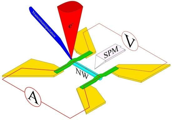
2. Materials and Methods
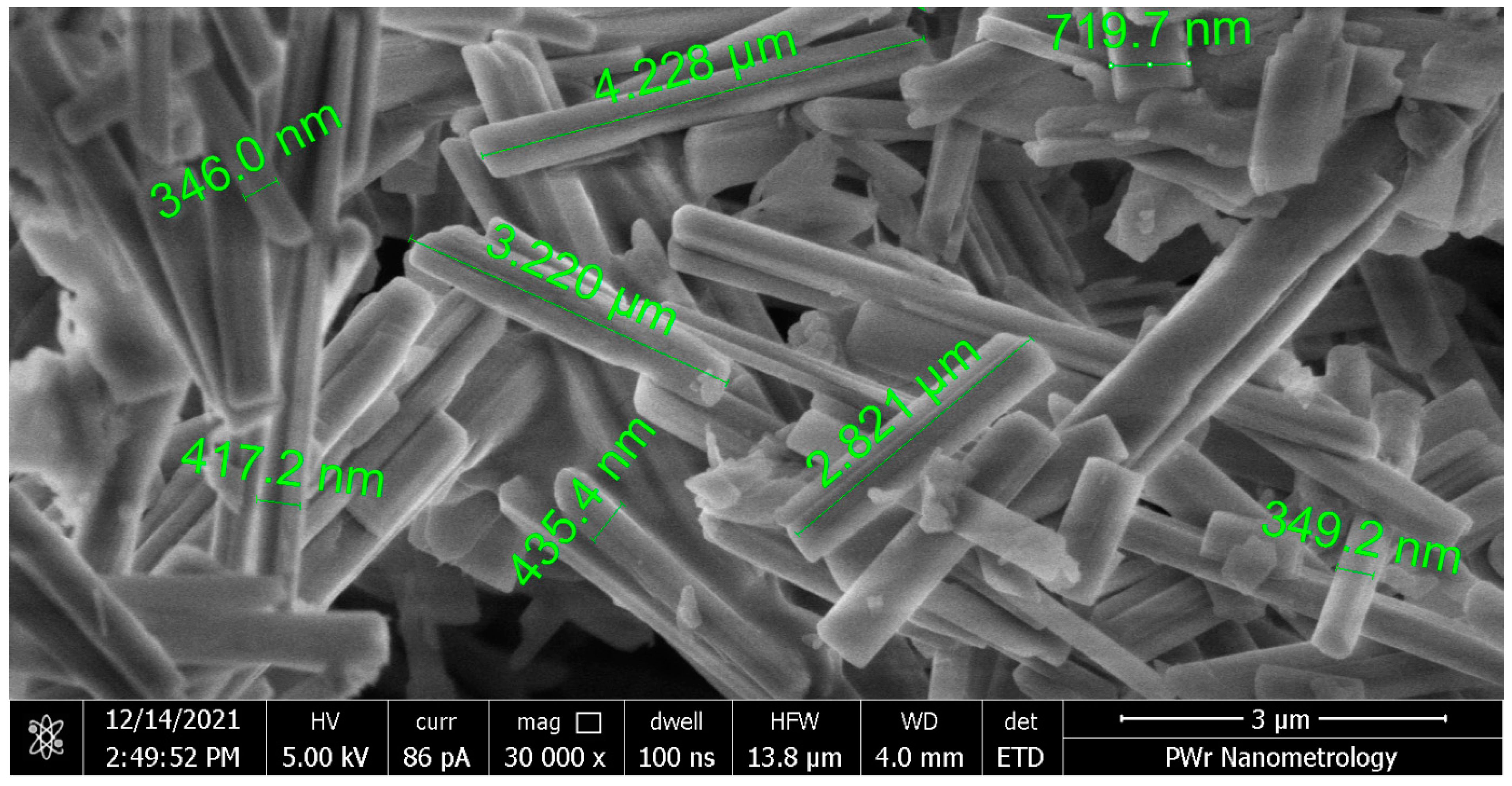
2.1. Nanowires
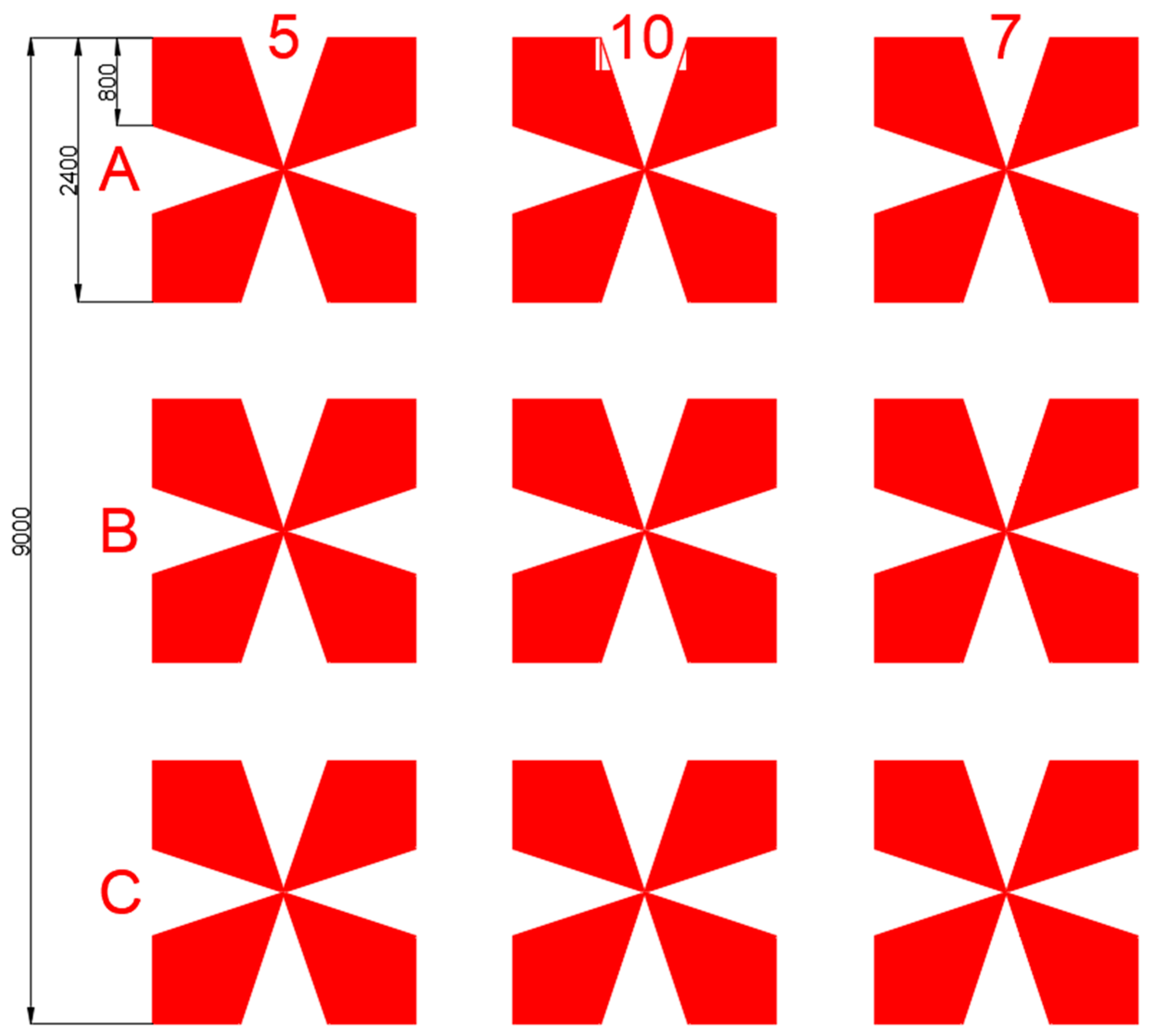
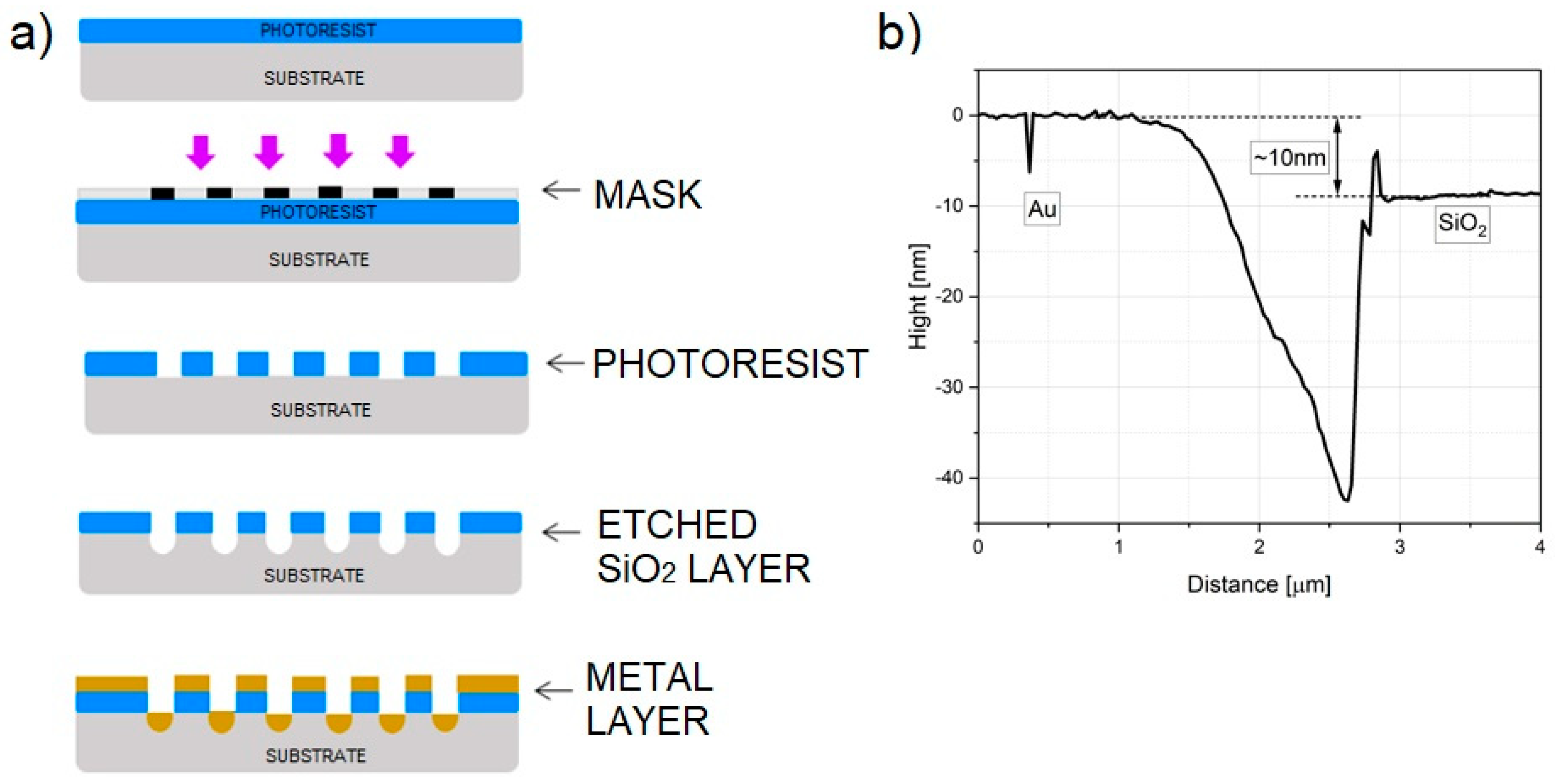
2.2. Measurement Substrates
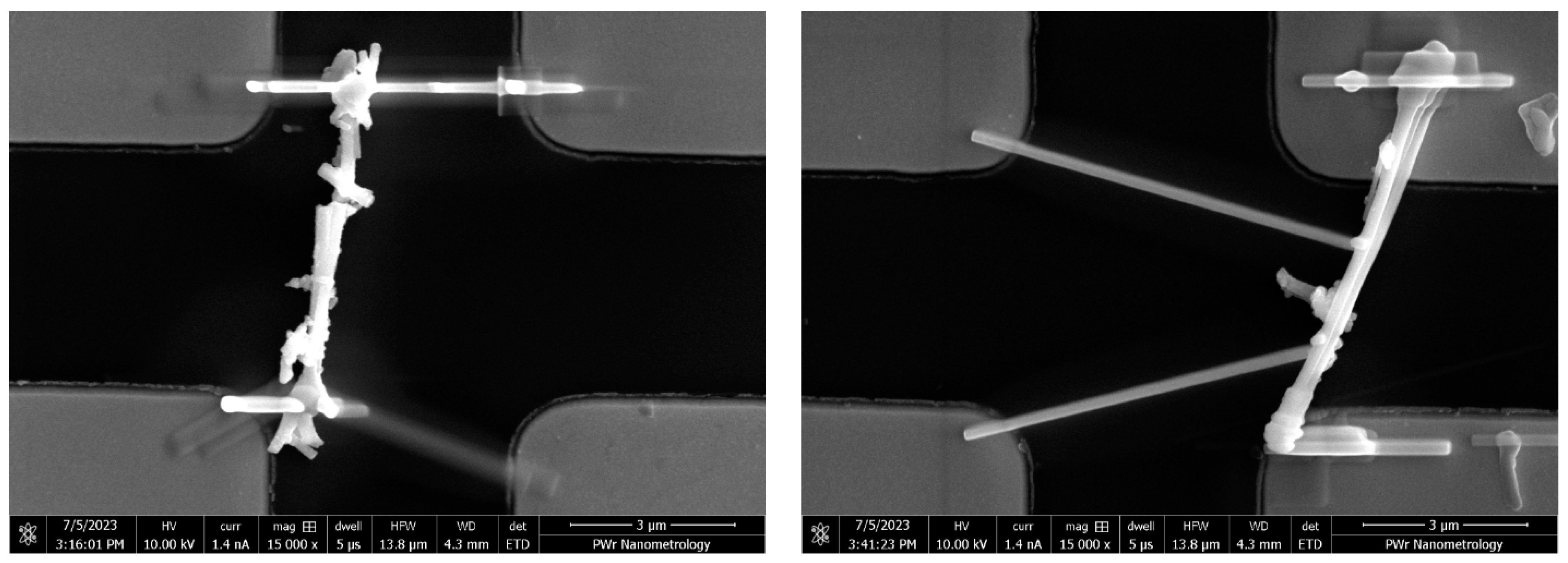
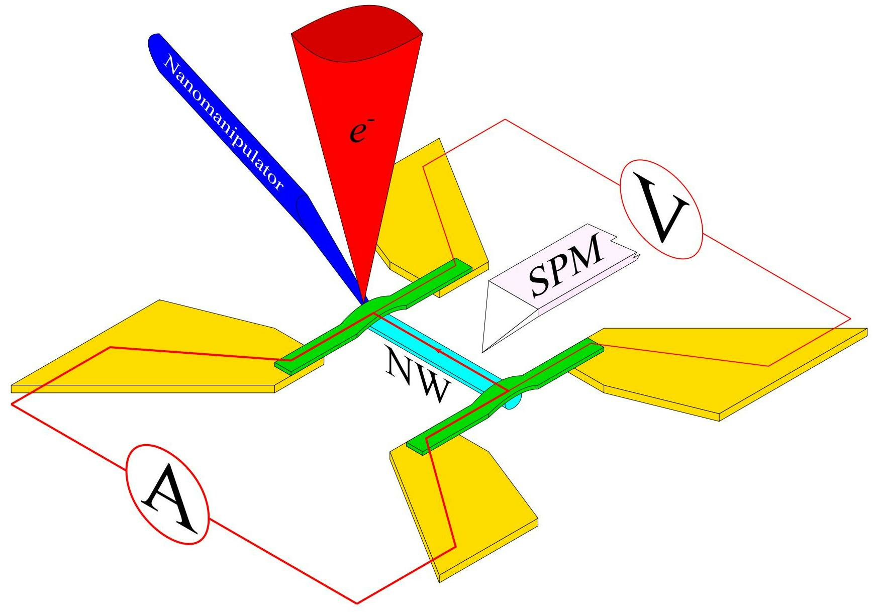
2.3. Nanowires Contacting
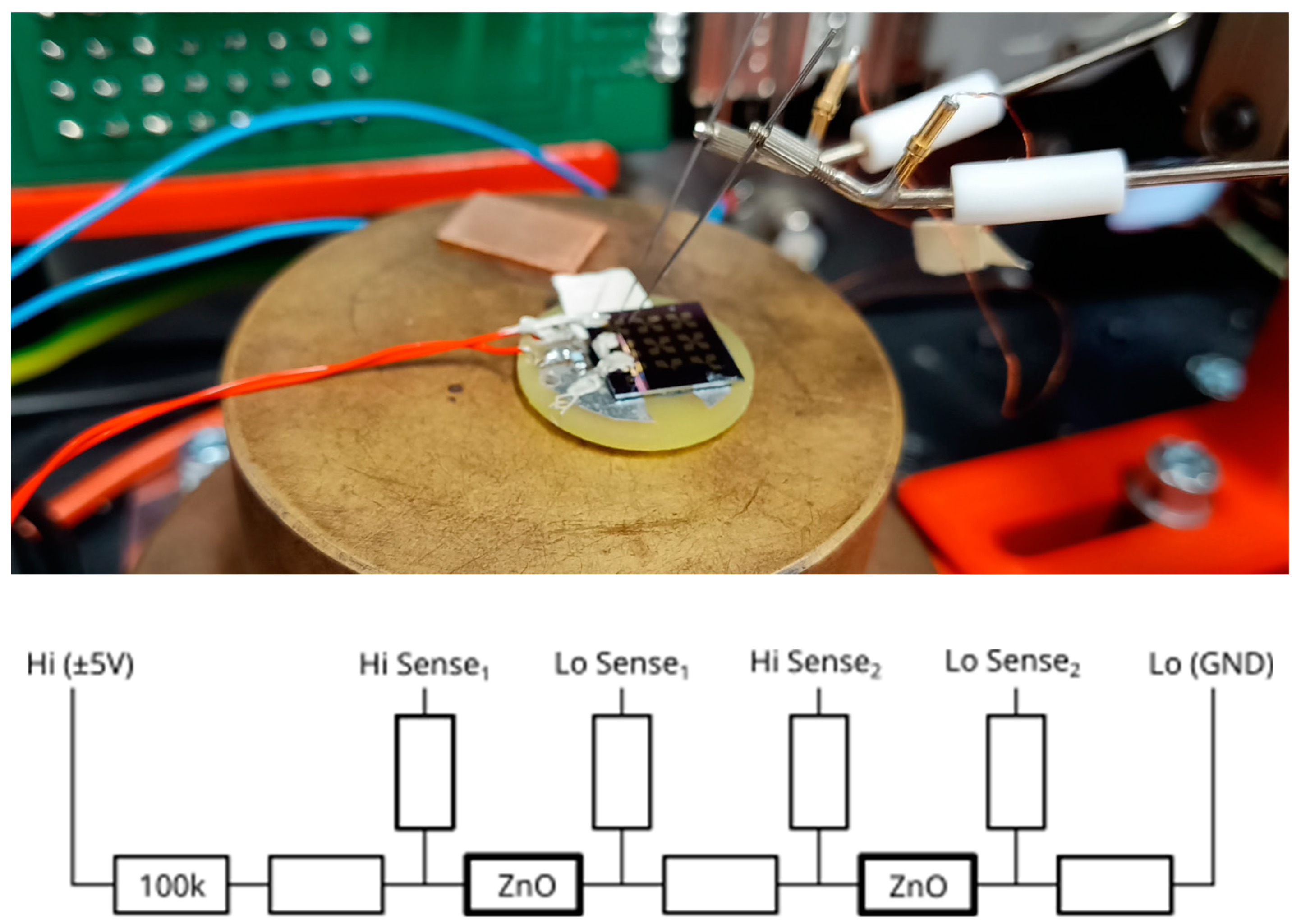
2.4. Electrical Measurements
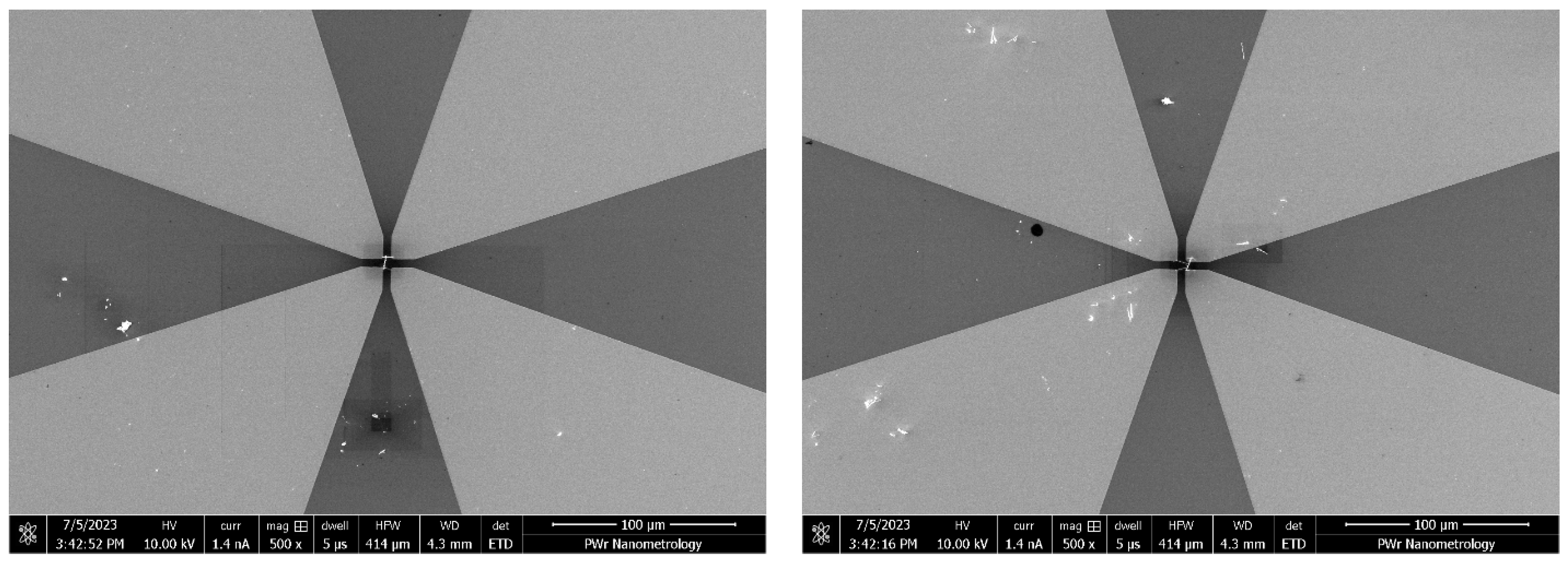
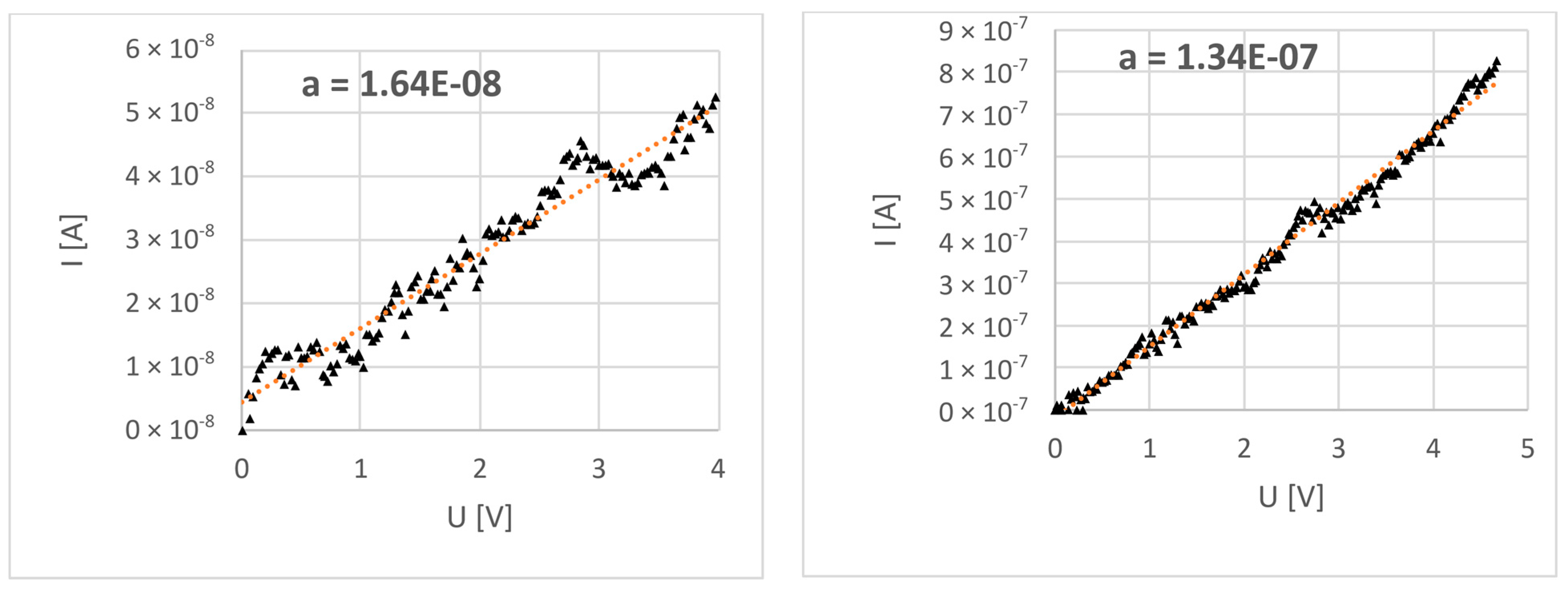
3. Results
4. Discussion
5. Conclusions
Author Contributions
Funding
Data Availability Statement
Acknowledgments
Conflicts of Interest
References
- Bieniek, T.; Janczyk, G.; Janus, P.; Grabiec, P.; Nieprzecki, M.; Wielgoszewski, G.; Moczała, M.; Gotszalk, T.; Buitrago, E.; Badia, M.F.-B.; et al. Silicon nanowires reliability and robustness investigation using AFM-based techniques. Electron. Technol. Conf. 2013, 8902, 89022L. [Google Scholar] [CrossRef]
- Jang, S.; Sung, J.; Chang, B.; Kim, T.; Ko, H.; Koo, K.-I.; Cho, D.-I. Characterization of the Piezoresistive Effects of Silicon Nanowires. Sensors 2018, 18, 3304. [Google Scholar] [CrossRef]
- Hur, S.; Lee, K.-H.; Hahn, Y.-B.; Kim, W.-D.; Choi, H. Power generation using piezoelectric ZnO nanowires for nano-scale devices. In Proceedings of the 10th IEEE International Conference on Nanotechnology, Ilsan, Korea, 17–20 August 2010; pp. 763–767. [Google Scholar] [CrossRef]
- Rojo, M.M.; Calero, O.C.; Lopeandia, A.F.; Rodriguez-Viejo, J.; Martín-Gonzalez, M. Review on measurement techniques of transport properties of nanowires. Nanoscale 2013, 5, 11526–11544. [Google Scholar] [CrossRef]
- Michels, T.; Rangelow, I.W. Review of scanning probe micromachining and its applications within nanoscience. Microelectron. Eng. 2014, 126, 191–203. [Google Scholar] [CrossRef]
- Ru, C.; Zhang, Y.; Sun, Y.; Zhong, Y.; Sun, X.; Hoyle, D.; Cotton, I. Automated Four-Point Probe Measurement of Nanowires Inside a Scanning Electron Microscope. IEEE Trans. Nanotechnol. 2010, 10, 674–681. [Google Scholar] [CrossRef]
- Janesch, J. Two-Wire vs. Four-Wire Resistance Measurements: Which Configuration Makes Sense for Your Application? Keithley Instruments Inc.: Cleveland, OH, USA, 2013. [Google Scholar]
- Nägelein, A.; Liborius, L.; Steidl, M.; Blumberg, C.; Kleinschmidt, P.; Poloczek, A.; Hannappel, T. Comparative analysis on resistance profiling along tapered semiconductor nanowires: Multi-tip technique versus transmission line method. J. Physics Condens. Matter 2017, 29, 394007. [Google Scholar] [CrossRef]
- He, H.; Hsin, L.; Liu, J.; Chen, J.; Wang, L. Piezoelectric Gated Diode of a Single ZnO Nanowire. Adv. Mater. 2009, 19, 781–784. [Google Scholar] [CrossRef]
- Ramanayaka, A.N.; Kim, H.-S.; Tang, K.; Wang, X.; Silver, R.M.; Stewart, M.D., Jr.; Pomeroy, J.M. STM patterned nanowire measurements using photolitographically defined implants in Si(100). Sci. Rep. 2018, 8, 1790. [Google Scholar] [CrossRef]
- Vinaji, S.; Lochthofen, A.; Mertin, W.; Regolin, I.; Gutsche, C.; Blekker, K.; Prost, W.; Tegude, F.J.; Bacher, G.; Caldas, M.; et al. Local Electrical Analysis of a Single Semiconductor Nanowire by Kelvin Probe Force Microscopy. AIP Conf. Proc. 2010, 1199, 329–330. [Google Scholar] [CrossRef]
- Cheng-Hao, C.; Ming-Hua, M.; Che-Wei, Y.; Hao-Hsiung, L. A New Analytic Formula for Minority Carrier Decay Length ex-traction from scanning Photocurrent Profiles in Ohmic-Contact Nanowire Devices. Sci. Rep. 2019, 9, 9426. [Google Scholar]
- Lin, R.; Bammerlin, M.; Hansen, O.; Schlittler, R.R.; Bøggild, P. Micro-four-point-probe characterization of nanowires fabricated using the nanostencil technique. Nanotechnology 2004, 15, 1363–1367. [Google Scholar] [CrossRef]
- Cronin, S.; Lin, Y.; Koga, T.; Sun, X.; Ying, J.; Dresselhaus, M. Thermoelectric investigation of bismuth nanowires. In Proceedings of the International Conference on Thermoelectrics (ICT), La Grande Motte, France, 17–21 August 2003; pp. 554–557. [Google Scholar] [CrossRef]
- Miccoli, I.; Edler, F.; Pfnur, H.; Tegenkamp, C.; Prete, P.; Lovergine, N. Surface-mediated electrical transport in single GaAs nanowires, 2015 1st Work. Nanotechnol. Instrum. Meas. NANOFIM 2018, 2015, 136–140. [Google Scholar] [CrossRef]
- Cardoza-Contreras, M.N.; Romo-Herrera, J.M.; Ríos, L.A.; García-Gutiérrez, R.; Zepeda, T.A.; Contreras, O.E. Single ZnO Nanowire-Based Gas Sensors to Detect Low Concentrations of Hydrogen. Sensors 2015, 15, 30539–30544. [Google Scholar] [CrossRef]
- Menke, E.J.; Brown, M.A.; Li, Q.; Hemminger, J.C.; Penner, R.M. Bismuth Telluride (Bi2Te3) Nanowires: Synthesis by Cyclic Electrodeposition/Stripping, Thinning by Electrooxidation, and Electrical Power Generation. Langmuir 2006, 22, 10564–10574. [Google Scholar] [CrossRef]
- Mølhave, K.; Wich, T.; Kortschack, A.; Bøggild, P. Pick-and-place nanomanipulation using microfabricated grippers. Nanotechnology 2006, 17, 2434–2441. [Google Scholar] [CrossRef]
- Zaraska, L.; Mika, K.; Syrek, K.; Sulka, G.D. Formation of ZnO nanowires during anodic oxidation of zinc in bicarbonate electrolytes. J. Electroanal. Chem. 2017, 801, 511–520. [Google Scholar] [CrossRef]
- Zaraska, L.; Mika, K.; Hnida, K.E.; Gajewska, M.; Łojewski, T.; Jaskuła, M.; Sulka, G.D. High aspect-ratio semiconducting ZnO nanowires formed by anodic oxidation of Zn foil and thermal treatment. Mater. Sci. Eng. B 2017, 226, 94–98. [Google Scholar] [CrossRef]
- Mika, K.; Wiercigroch, E.; Pisarek, M.; Kozieł, M.; Majda, D.; Lytvynenko, A.S.; Sulka, G.D.; Zaraska, L. Nanostructured films formed on Zn during anodic oxidation in different carbonate-based electrolytes. Appl. Surf. Sci. 2023, 623, 157102. [Google Scholar] [CrossRef]
- Paiman, S.; Ling, T.H.; Husham, M.; Sagadevan, S. Significant effect on annealing temperature and enhancement on structural, optical and electrical properties of zinc oxide nanowires. Results Phys. 2020, 17, 103185. [Google Scholar] [CrossRef]
- Cronin, S.B.; Lin, Y.M.; Koga, T.; Ying, J.Y.; Dresselhaus, M.S. Transport Measurements of Individual Bi Nanowires. MRS Proc. 1999, 582, 13–18. [Google Scholar] [CrossRef]
- Farrance, I.; Frenkel, R. Uncertainty of Measurement: A Review of the Rules for Calculating Uncertainty Components through Functional Relationships. Clin. Biochem. Rev. 2012, 33, 49–75. [Google Scholar]
- Lord, A.M.; Maffeis, T.G.; Walton, A.S.; Kepaptsoglou, D.M.; Ramasse, Q.M.; Ward, M.B.; Köble, J.; Wilks, S.P. Factors that determine and limit the resistivity of high-quality individual ZnO nanowires. Nanotechnology 2013, 24, 435706. [Google Scholar] [CrossRef]
- Schlenker, E.; Bakin, A.; Weimann, T.; Hinze, P.; Weber, D.H.; Gölzhäuser, A.; Wehmann, H.-H.; Waag, A. On the difficulties in characterizing ZnO nanowires. Nanotechnology 2008, 19, 365707. [Google Scholar] [CrossRef]
- Yi, G.-C.; Wang, C.; Park, W.I. ZnO nanorods: Synthesis, characterization and applications. Semicond. Sci. Technol. 2005, 20, S22–S34. [Google Scholar] [CrossRef]
- He, J.H.; Lao, C.S.; Chen, L.J.; Davidovic, D.; Wang, Z.L. Large-Scale Ni-Doped ZnO Nanowire Arrays and Electrical and Optical Properties. J. Am. Chem. Soc. 2005, 127, 16376–16377. [Google Scholar] [CrossRef]


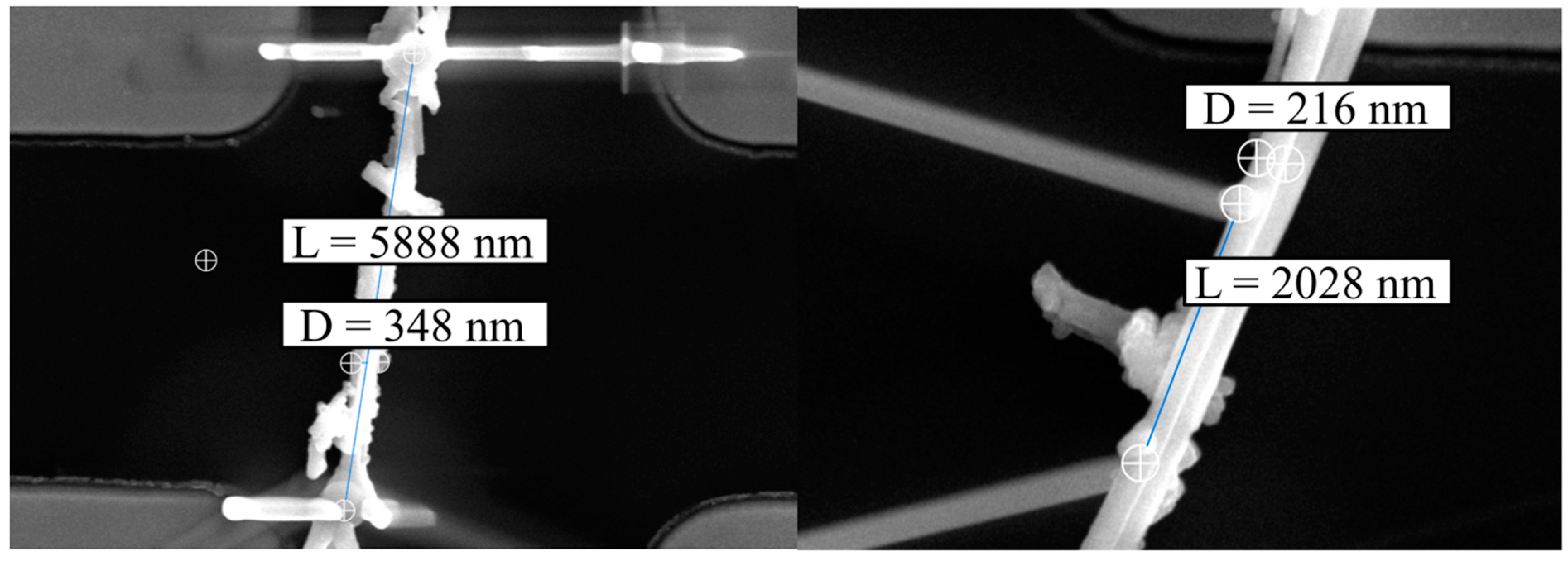
| Annealed Sample | Length (nm) | Diameter (nm) | Resistance (MΩ) | Resistivity (Ωm) |
|---|---|---|---|---|
| 200 °C | 5888 ± 50 | 348 ± 20 | 74.8 ± 1.25 | 3.9 ± 0.46 |
| 300 °C | 2028 ± 50 | 216 ± 20 | 6 ± 0.11 | 0.55 ± 0.11 |
Disclaimer/Publisher’s Note: The statements, opinions and data contained in all publications are solely those of the individual author(s) and contributor(s) and not of MDPI and/or the editor(s). MDPI and/or the editor(s) disclaim responsibility for any injury to people or property resulting from any ideas, methods, instructions or products referred to in the content. |
© 2023 by the authors. Licensee MDPI, Basel, Switzerland. This article is an open access article distributed under the terms and conditions of the Creative Commons Attribution (CC BY) license (https://creativecommons.org/licenses/by/4.0/).
Share and Cite
Pruchnik, B.C.; Fidelus, J.D.; Gacka, E.; Kwoka, K.; Pruchnik, J.; Piejko, A.; Usydus, Ł.; Zaraska, L.; Sulka, G.D.; Piasecki, T.; et al. Four-Point Measurement Setup for Correlative Microscopy of Nanowires. Nanomaterials 2023, 13, 2451. https://doi.org/10.3390/nano13172451
Pruchnik BC, Fidelus JD, Gacka E, Kwoka K, Pruchnik J, Piejko A, Usydus Ł, Zaraska L, Sulka GD, Piasecki T, et al. Four-Point Measurement Setup for Correlative Microscopy of Nanowires. Nanomaterials. 2023; 13(17):2451. https://doi.org/10.3390/nano13172451
Chicago/Turabian StylePruchnik, Bartosz C., Janusz D. Fidelus, Ewelina Gacka, Krzysztof Kwoka, Julia Pruchnik, Adrianna Piejko, Łukasz Usydus, Leszek Zaraska, Grzegorz D. Sulka, Tomasz Piasecki, and et al. 2023. "Four-Point Measurement Setup for Correlative Microscopy of Nanowires" Nanomaterials 13, no. 17: 2451. https://doi.org/10.3390/nano13172451
APA StylePruchnik, B. C., Fidelus, J. D., Gacka, E., Kwoka, K., Pruchnik, J., Piejko, A., Usydus, Ł., Zaraska, L., Sulka, G. D., Piasecki, T., & Gotszalk, T. P. (2023). Four-Point Measurement Setup for Correlative Microscopy of Nanowires. Nanomaterials, 13(17), 2451. https://doi.org/10.3390/nano13172451