Article

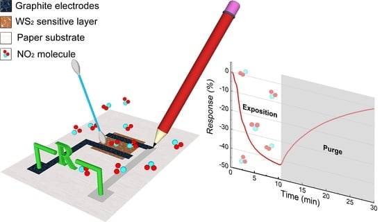
Eco-Friendly Disposable WS2 Paper Sensor for Sub-ppm NO2 Detection at Room Temperature

by
Daniel Matatagui
1,*,
Carlos Cruz
1,
Felix Carrascoso
2,
Abdullah M. Al-Enizi
3,
Ayman Nafady
3,
Andres Castellanos-Gomez
2,* and
María del Carmen Horrillo
1
1
Grupo de Tecnología de Sensores Avanzados (SENSAVAN), Instituto de Tecnologías Físicas y de la Información (ITEFI), CSIC, 28006 Madrid, Spain
2
Materials Science Factory, Instituto de Ciencia de Materiales de Madrid (ICMM-CSIC), 28049 Madrid, Spain
3
Department of Chemistry, College of Science, King Saud University, Riyadh 11451, Saudi Arabia
*
Authors to whom correspondence should be addressed.
Nanomaterials 2022, 12(7), 1213; https://doi.org/10.3390/nano12071213
Submission received: 16 March 2022 / Revised: 28 March 2022 / Accepted: 1 April 2022 / Published: 5 April 2022
(This article belongs to the Special Issue 2D Materials and Their Heterostructures and Superlattices II)

Abstract

:
We developed inexpensive and disposable gas sensors with a low environmental footprint. This approach is based on a biodegradable substrate, paper, and features safe and nontoxic electronic materials. We show that abrasion-induced deposited WS2 nanoplatelets on paper can be employed as a successful sensing layer to develop high-sensitivity and selective sensors, which operate even at room temperature. Its performance is investigated, at room temperature, against NO2 exposure, finding that the electrical resistance of the device drops dramatically upon NO2 adsorption, decreasing by ~42% (~31% half a year later) for 0.8 ppm concentration, and establishing a detection limit around~2 ppb (~3 ppb half a year later). The sensor is highly selective towards NO2 gas with respect to the interferents NH3 and CO, whose responses were only 1.8% (obtained for 30 ppm) and 1.5% (obtained for 8 ppm), respectively. Interestingly, an improved response of the developed sensor under humid conditions was observed (tested for 25% relative humidity at 23 °C). The high-performance, in conjunction with its small dimensions, low cost, operation at room temperature, and the possibility of using it as a portable system, makes this sensor a promising candidate for continuous monitoring of NO2 on-site.

Graphical Abstract

1. Introduction

Gas sensing is becoming more and more important in our society. In fact, detection of various gases in low concentrations is crucial (and sometimes even mandatory) in fields such as air quality assessment, greenhouse gas emissions control, the quantification of volatiles for smart maintenance in the industry sector, and identification of biomarkers in medical diagnosis [1,2,3,4,5].
Among the gaseous species that should be monitored, detection of nitrogen dioxide (NO2) is required in different applications. In the atmosphere, NO2 plays the role of greenhouse gas and causes acid rain and photochemical smog problems [6]. Long-term exposure to high levels of NO2 produces harmful effects for humans and other living beings [7,8]. Additionally, nitrogen oxides (NOx) in exhaled breath are biomarkers for inflammatory and oxidative changes in lungs, serving as early indicators of the pathophysiology of many respiratory diseases [9].
Chemical sensors based on semiconductor materials [10,11,12,13,14,15], and particularly metal oxides, are the most popular devices to sense NO2 gas [16,17,18,19]. However, these metal-oxide-based devices present poor sensitivity at room temperature, requiring high-temperature operation that leads to high power consumption and the eventual degradation of the sensing material [20]. Moreover, metal-oxide devices require the use of substrates compatible with micro-fabrication techniques (i.e., silicon, glass, quartz, etc.), which hampers their application in disposable electronics applications where the use of ultra-low cost and biodegradable substrates is crucial to emerging technologies and environmental impacts.
Over the past two decades, thanks to the revival of interest in van der Waals materials aroused by the isolation of graphene [21], sensors based on layered materials have been presented as a real step forward in gas sensing. Their exceptionally large surface-area-to-volume ratio makes these materials strongly sensitive to adsorbed gases, and therefore they are promising candidates for gas detection [22,23,24,25,26,27,28]. In fact, over the last years, several examples of NO2 gas sensors based on van der Waals materials, operating even at room temperature, have been proved [26,29,30,31,32].
The attractive properties of the conventional printer paper as a substrate, mainly its environmental-friendliness and low-cost, have led researchers to develop paper-based devices for various applications, including memory devices [33], solar cells [34,35], RFID-enabled wireless sensors [36], or supercapacitors [37]. Recently, some of the authors have demonstrated the integration of van der Waals materials on paper substrates through direct abrasion against the rough surface of paper [38,39,40,41]. However, only light and temperature sensors have been demonstrated so far, with gas sensing remaining unexplored. Because of the combination of ultra-low cost, availability, and biodegradability of paper substrates, integrating van der Waals materials on paper substrates opens the door for low-cost and disposable [42,43,44,45,46,47,48,49,50] gas sensors.
Here, we demonstrate the fabrication of gas sensors on standard copy paper substrates using abrasion-induced deposited WS2 films as a sensing material. This process is simple to implement and yields low-cost and environmentally-friendly devices. In fact, standard copy paper substrates are biodegradable, and the sensing film (WS2) and electrodes (graphite) are safe, nontoxic materials that can be found as natural minerals on Earth’s crust. The sensing performance of the WS2-based sensor under exposure to NO2 gas, operating at room temperature, is examined. Furthermore, the selectivity relative to potential interfering gases (NH3 and CO) is analyzed [51,52,53].

2. Materials and Methods

2.1. Materials

Standard (untreated) copy printer paper (80 g/m2) was used as supporting substrates because of its low cost and availability. Tungsten disulfide (WS2) from HAGEN automation Ltd. (Bedford, UK) (0.6 microns APS Ultra Grade Micronized) was used as gas sensing channel material. Among the different semiconducting transition metal dichalcogenides, we selected WS2 as it yielded films with the lower electrical resistance facilitating the electrical read-out of the fabricated devices. Graphite pencil (Madrid, Spain) (4B, Faber Castell) was employed to pattern graphite-based electrical leads (it has ~80% of graphite content [54]) to connect the WS2 channel to the readout electronics.

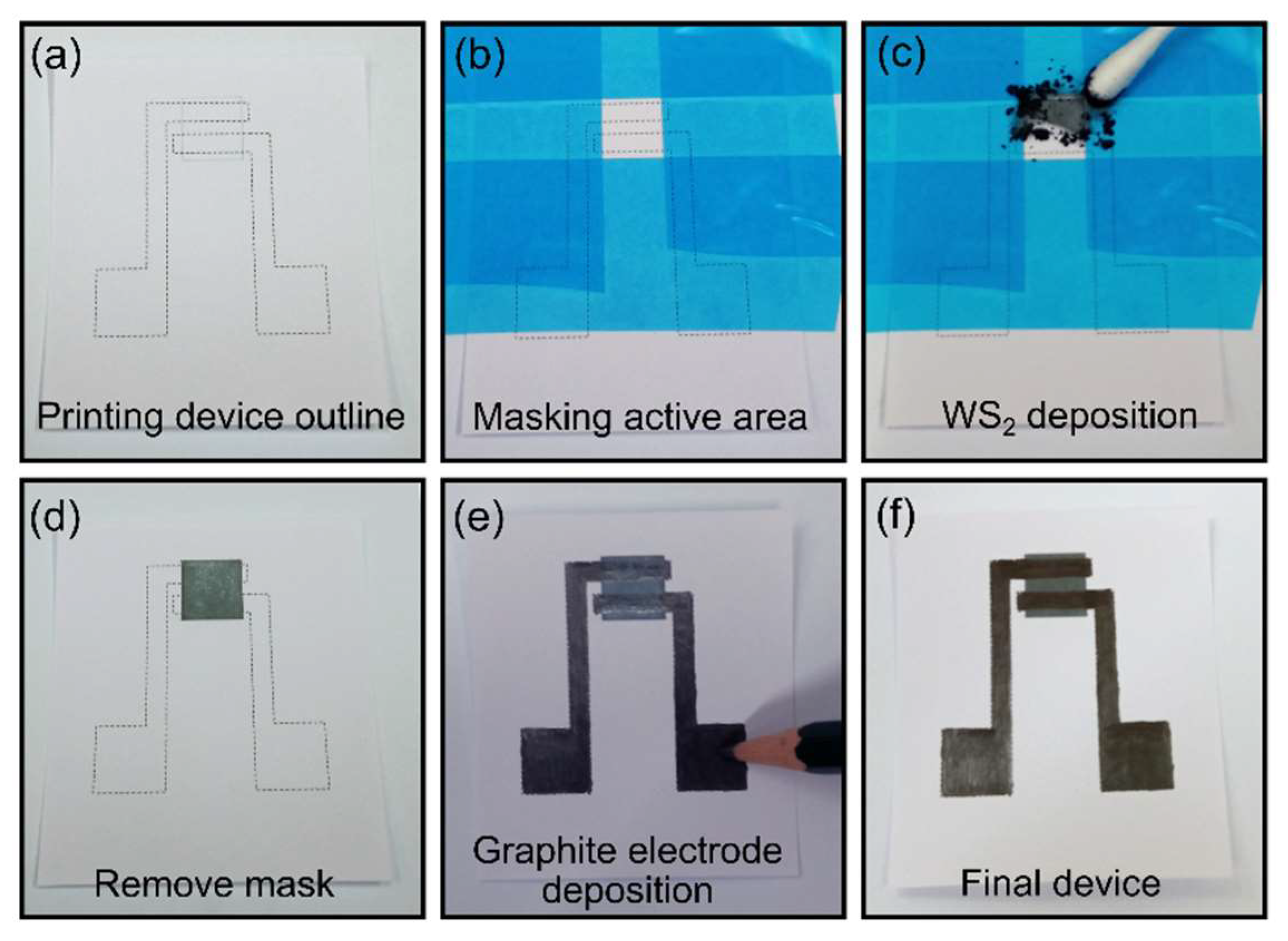
2.2. Sensor Fabrication

The steps for the gas sensor fabrication are depicted in Figure 1. First, the outline of the sensitive layer channel and electrodes were printed on the paper substrate (Figure 1a). Then, a stencil mask (made of Nitto SPV 224 tape) delimited the sensitive area (Figure 1b). Micronized WS2 powder was rubbed against the unmasked paper substrate with a cotton swab (Figure 1c). The depositing process mimics the action of drawing/writing with a pencil on paper, where the friction forces between the van der Waals materials and paper cleaves the van der Waals crystals, leading to a network of interconnected platelets. The powder was abraded until a continuous film was reached. Then, the excess powder and the stencil mask were removed (Figure 1d). In the last process step, graphite electrodes were deposited on top of the sensitive material by drawing directly with a high-graphite content pencil (Figure 1e). These electrodes were contacted with spring-loaded probes (pogo pins) integrated inside the test chamber. Figure 1f shows a picture of the final device.

2.3. Material Characterization

Scanning electron microscopy (SEM) and energy dispersive X-ray spectroscopy (EDX), using a FE-SEM, FEI Nova NANOSEM 230 (Hillsboro, OR, USA), were used to characterize the morphology and the composition of the WS2 films deposited on paper. An electron energy of 7 keV was employed for imaging and 14 keV for EDX spectroscopy.

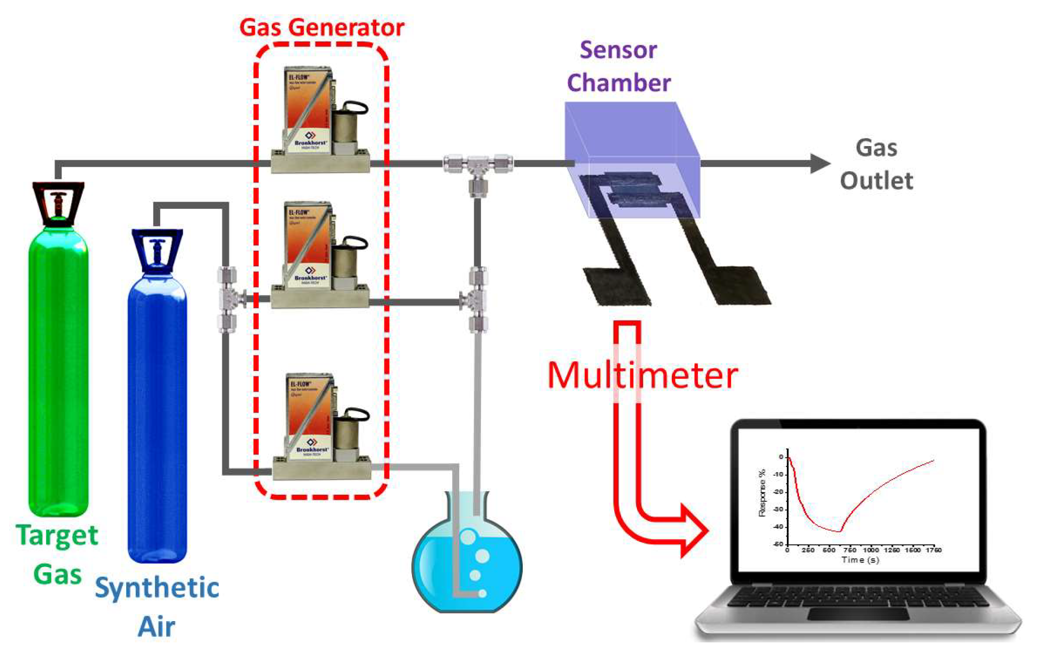
2.4. Experimental Setup

The chemoresistive sensor was placed inside a 6.25 mL volume airtight chamber for its characterization in different reducing and oxidizing atmospheres. Airflow inside the chamber was set to 100 mL/min, switching between gas sample for 10 min (exposition time) and synthetic air for 20 min (purge time). Gas cylinders supplied target gases with appropriate concentrations and balanced with the carrier gas (synthetic air): NO2 (1 ppm), CO (10 ppm), and NH3 (50 ppm) (all of them from Nippon Gases). Then, the initial sample concentration was diluted with synthetic air by using a gas mixing unit (GMU, Ray IE, Cáceres, Spain)to obtain the required exposed concentration. For proper control of the relative humidity (RH) inside the chamber, a handheld thermohygrometer RS1364 was used. The temperature was kept at 23 °C during the tests, and the required RH was achieved with a third flow controller that regulates the synthetic air bubbling through deionized water (Figure 2).
The sensor was kept at room temperature while variations of the resistance over time were recorded with a digital multimeter (Keithley 2001). The experiment control and real time data acquisition was implemented with a PC using an in-house custom-made software developed with LabVIEW. The response of the sensor was calculated with the following equation:
R e s p o n s e = Δ R / R 0 = ( R R 0 ) / R 0
where R is the electrical resistance for the sensor in the tested gas and R 0 is the resistance of the sensor in the air.

3. Results

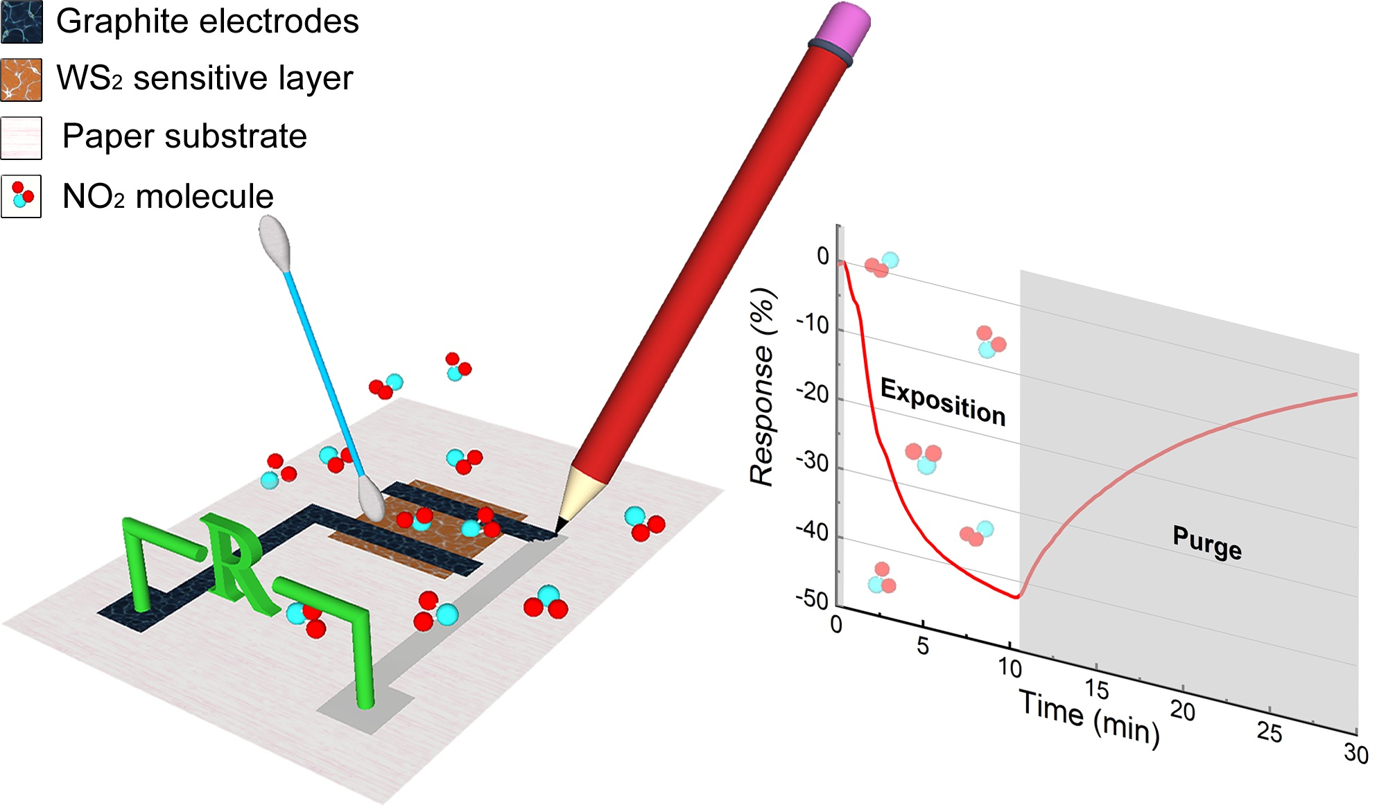
3.1. Structural and Morphological Characterization

Figure 3a shows SEM image of the cross-section of the WS2 flakes forming the micronized WS2 powder. The flakes are initially 5–10 µm in lateral size and 50–150 nm thick. Figure 3b shows a SEM image of the porous microscopic structure of the WS2 film deposited onto the paper substrate, formed by interconnected crystalline WS2 platelets, ensuring a very large effective surface area of the device. During the abrasion process, the WS2 flakes are cleaved, reducing their lateral dimensions to 1–5 µm and their thickness to sub-50 nm. Figure 3c shows a low magnification SEM image of a WS2 film obtained after its deposition on the paper substrate. The bare paper has fibrous-like structures arising from the cellulose fibers. The abrasion-induced deposition method yielded a continuous film of packed WS2 platelets covering the fibers. The bare paper and WS2 film can be easily distinguished because of their different contrast under SEM inspection. Figure 3d shows a SEM image of the sensitive area/electrode interface where it can be observed a sizable change in contrast due to the difference in electrical conductivity between the WS2 film and the WS2 film covered with graphite. The chemical composition of the film was characterized by energy dispersive X-ray (EDX) spectroscopy. Apart from the prominent W and S peaks, expected from the WS2 film, the spectrum had peaks associated with the presence of C and O, arising from the paper substrate. The spectrum also showed a Ca peak, attributed to the presence of calcium carbonate, a filler usually added to paper pulp to achieve a brighter white color (Figure 3e).

3.2. Electrical Characterization

A thorough characterization of the electrical properties of abrasion-induced deposited WS2 films on copy paper can be found in Ref [41]. Briefly, the resistivity of the films, determined through current vs. voltage measurements in transfer length configuration, ranges from ~360 Ω·m to ~530 Ω·m and electric field effect measurements demonstrated the p-type character of the WS2 film. Additionally, in the mentioned reference, 118 devices were developed to study the reproducibility, showing a low dispersion taking into account the nature of the films: a random network of interconnected platelets where percolation transport is expected.
The sensor was kept at air atmosphere, and after a few minutes, the calculated root-mean square (RMS) noise level was approximately 0.01% for the sensor. Thanks to the electrical continuity of the WS2 film, the device operates with low noise that is a consequence of the dry deposition method, and a good adhesion between sensitive material and paper fibers.

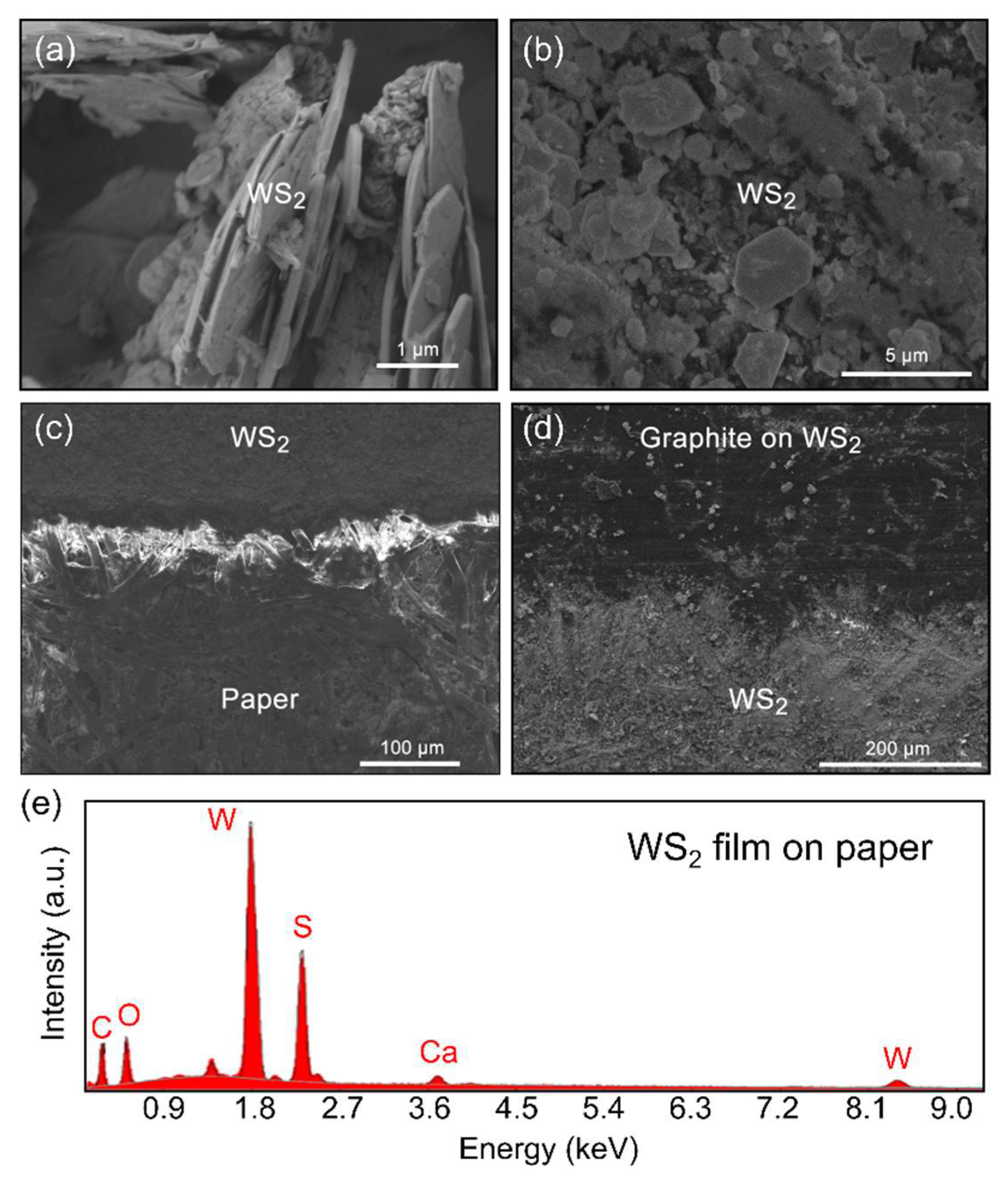
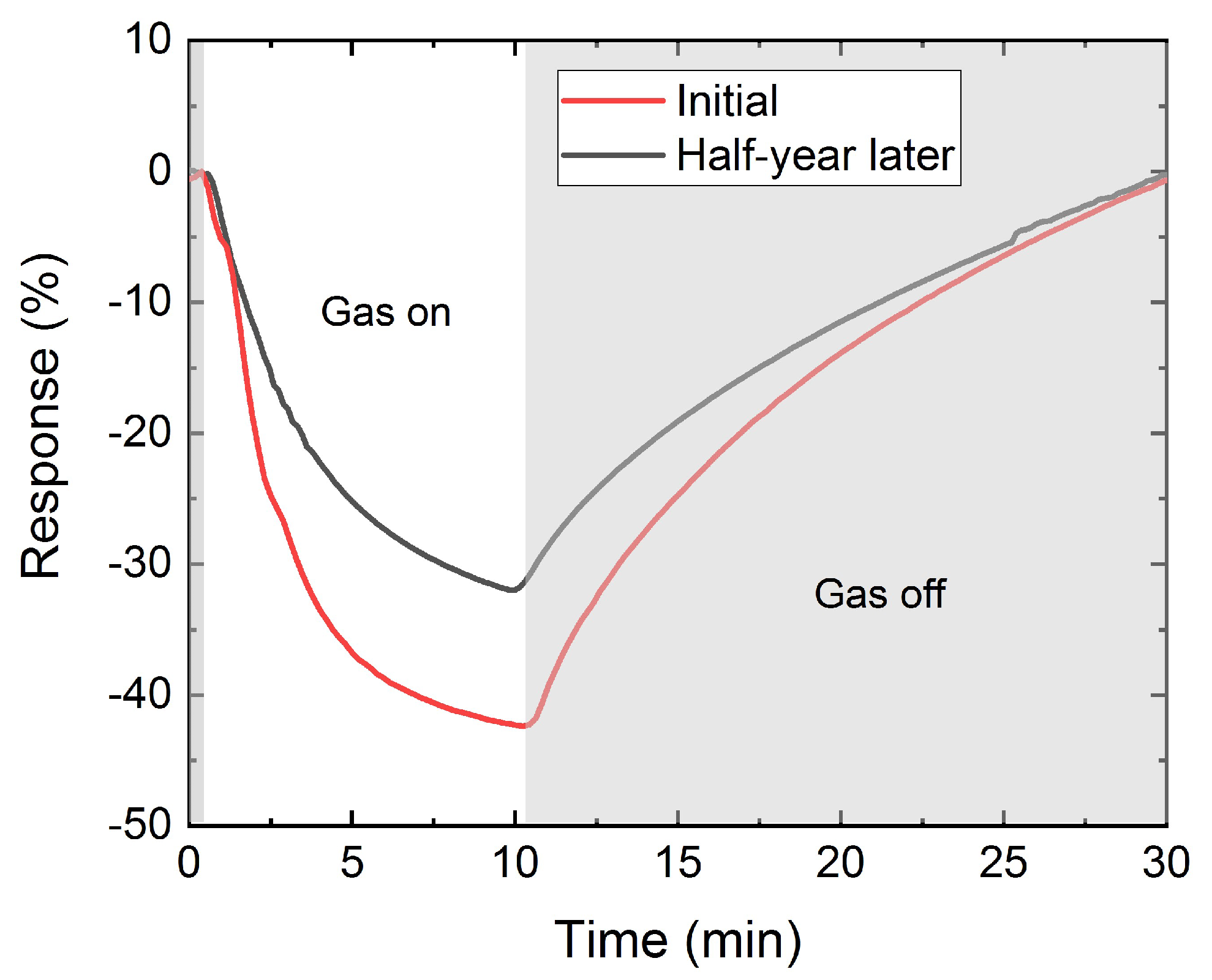
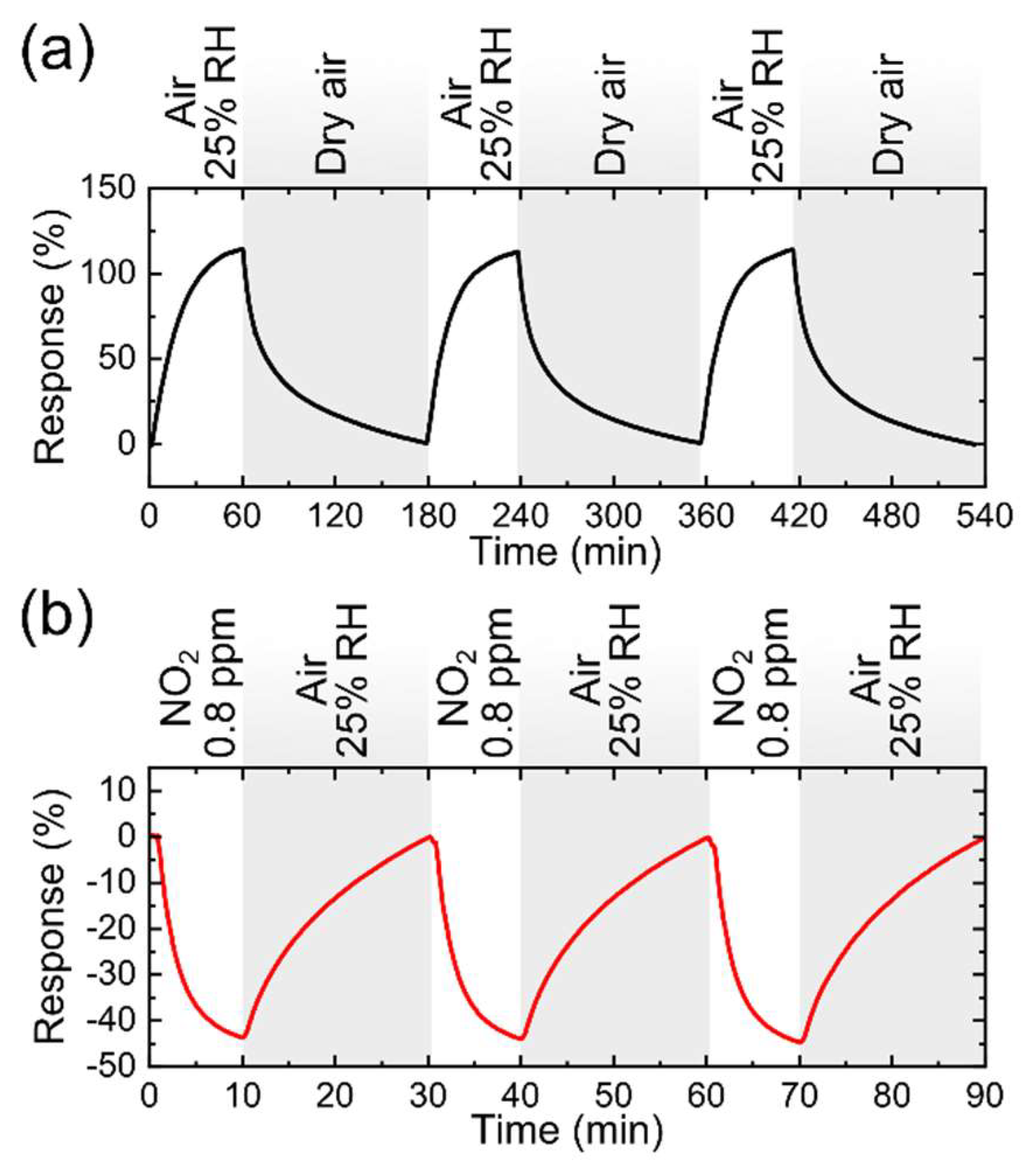
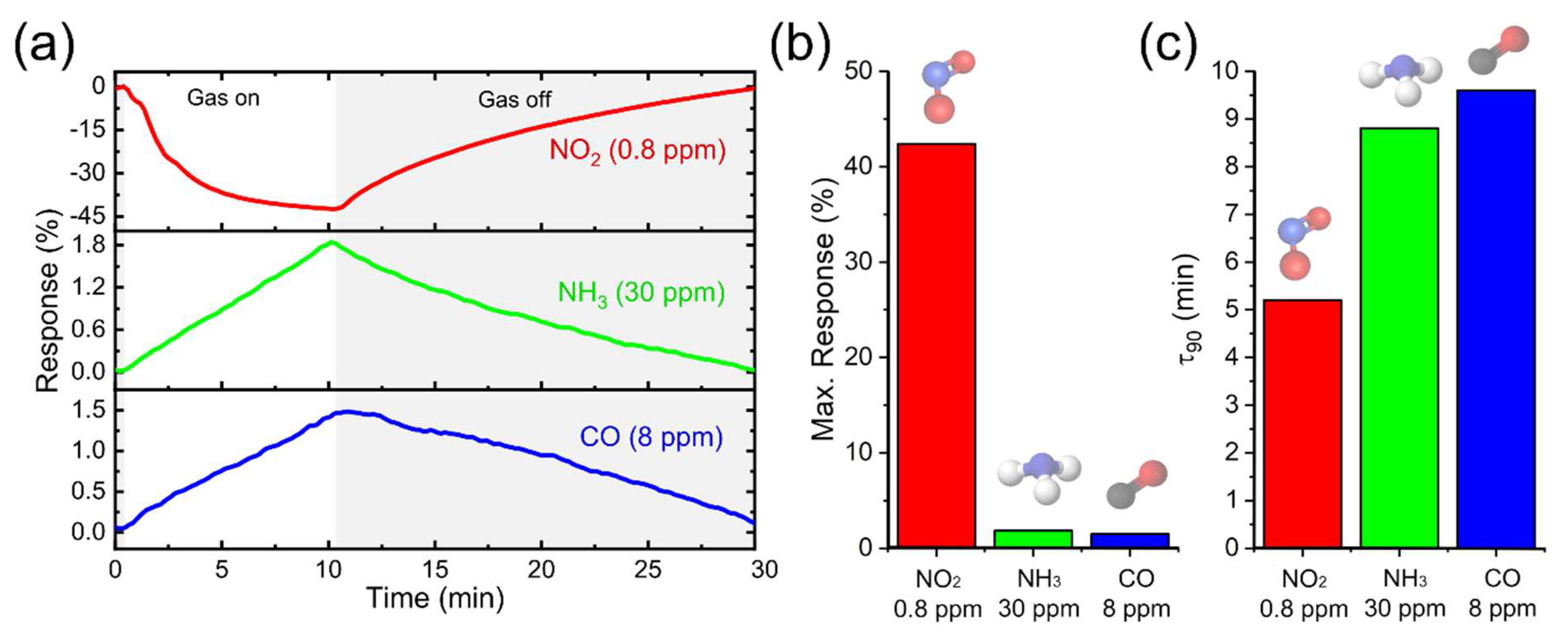
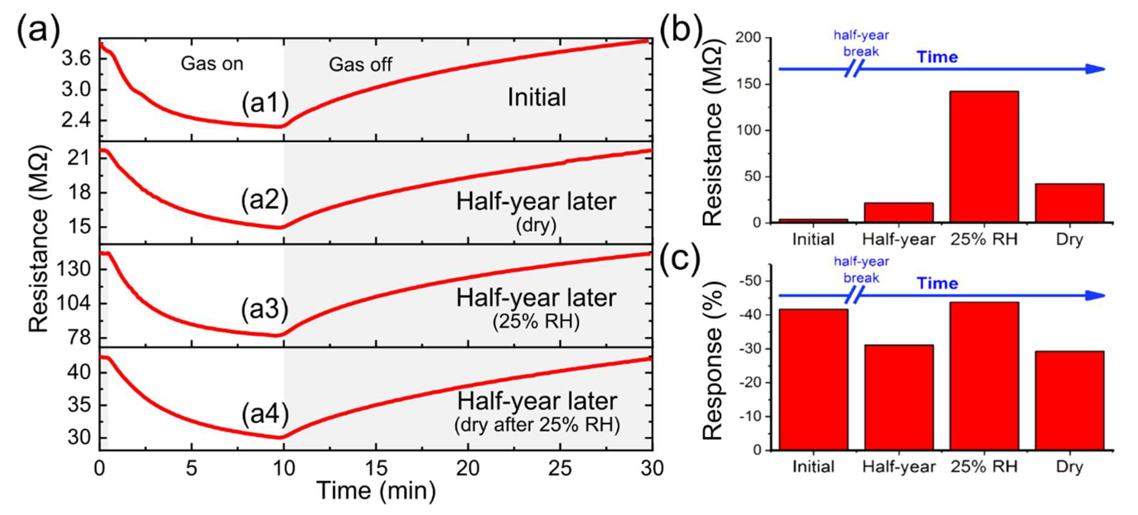
3.3. Gas Sensor Characterization

To characterize the performance of this sensor, its sensitivity, and response time, we studied the changes in resistance upon cyclic exposition and purge processes with NO2 at various concentrations ranges (0.2 ppm–0.8 ppm, see Figure 4a). The gas sensing mechanism is attributed to the surface reactions between the p-type WS2 platelets and gas molecules. In the case of a p-type semiconductor in an oxidant environment (NO2), the concentration of electrons on the surface decreases (the number of holes increases) and, consequently, the resistance of the WS2 film decreases (Figure 4a). The sensor device showed a fast recovery with a low baseline drift of 0.6% at 0.8 ppm of NO2. Therefore, an automatic baseline subtraction method based on linear correction for measurements before exposition and in the final of the purge time was implemented.
In most real-life applications, the target gas is in a complex environment surrounded by several gases at different concentrations, requiring sensors with high sensitivity and selectivity to discriminate and classify the target gas. Important interfering gases, in the above applications, are carbon monoxide (CO) and ammonia (NH3) [55,56]. Therefore, gas sensors with negligible interference between reducing and oxidizing environments, i.e., a high absolute selectivity, are highly desirable to achieve a more reliable signal interpretation. To test the selectivity of the WS2 on paper NO2 sensor, we have subjected the device to cyclic exposition and purge processes with CO and NH3 at various concentrations ranges (1.5 ppm–8 ppm for CO and 10 ppm–30 ppm for NH3, see Figure 4b,c). Upon exposure to CO and NH3, the resistance increases as expected for a p-type semiconductor, because the generated electrons recombine with holes. The gas test showed the sensor has a remarkably higher sensitivity towards NO2 (42% resistance change at 0.8 ppm) than NH3 and CO, whose responses were 1.8% (obtained at 30 ppm) and 1.5% (obtained at 8 ppm), respectively (see Figure 5a,b). This can be justified by the adsorption kinetics of gas molecules on the sensitive material. Additionally, the high sensitivity and selectivity to NO2 is consistent with results of density functional theory calculation in Ref. [32]. Interestingly, this article explains that the chemically reactive edge sites of WS2 served as highly favorable active sites for direct interaction with target NO2 gas molecules. This is consistent with the fact that abrasion-induced is an effective method to generate numerous edge sites in deposited WS2 nanoplatelets on paper, since the technique induces fracturing, tearing, and peeling off from substrates.
Accordingly, the response speed of the device was studied. We determined the response time parameter τ90, defined as the time necessary to reach approximately 90% of the response when the sensor is subjected to an abrupt change in atmosphere. The τ90 values obtained were NO2 5.2 min at 0.8 ppm, NH3 8.8 min at 30 ppm, and CO 9.6 min at 8 ppm (Figure 5c). In comparison, the paper-based sensor showed the shortest response time for NO2 that nearly achieved the equilibrium. In contrast, CO and NH3 responses had not yet approached an equilibrium, resulting in a high sensitivity NO2 gas sensor with insignificant NH3/CO-interference. Therefore, this very high selectivity with respect to potential interfering gases of the sensor is highly advantageous to be used for gas sensing applications.
The structural continuity of the micronized WS2 particles deposited by abrasion provides higher electrical conductivity toward a lower limit of detection (LOD) compared to sensors fabricated by other methods, such as drop-casting [26]. From the response for 0.8 ppm of NO2, a theoretically achievable LOD of around 2 ppb was calculated, which is equivalent to a signal-to-noise ratio (SNR) value of three.
In order to assess the stability of these devices upon environmental degradation, we performed a new set of measurements half a year after its fabrication (the sensor was stored under ambient conditions during that time). Thereafter, the response for 0.8 ppm of NO2 was slightly decreased to 31%, increasing the LOD around 3 ppb (Figure 6). In particular, the decrease of the gas response is small between measurements for a half year interval, which demonstrates that the paper-based sensor has a slow degradation, maintaining a high response over time. The effect of relative humidity on the paper-based sensor was tested at 23 °C with 25% RH and it responded efficiently to humidity, obtaining a maximum response of 114% (Figure 7a). Cross-sensitivity measurements were carried out to assess the influence of RH on the sensor response to NO2. Figure 7b illustrates the effect of 0.8 ppm of NO2 detection in an environment with a RH of 25% with a sensor response of ~44%.
The experimental responses of NO2 over time and under humid conditions were compared for 0.8 ppm (Figure 8a1–a4). In the days following device manufacture, the sensor had a high response close to 42% with an operating resistance of ~4 MΩ. Then, after half a year where the sensor was stored in ambient conditions, the resistance increased to ~22 MΩ, decreasing the response to ~31%, which was attributed to the effects of sensor poisoning by gases surrounding in ambient during the half a year period. However, a positive effect of humid conditions (25% RH at 23 °C) is that at the same gas concentration the sensor response increased to 44%, simultaneously the resistance scaled up ~142 MΩ. The improved response to NO2 with humidity can be justified by the intrinsic and induced dipole moments of the molecules and their intermolecular charge transfer [57]. Finally, there was a practically total regeneration of the sensor after humidity exposition was obtained for dry synthetic air, and the sensor showed a response of ~30% for a resistance operation of ~42 MΩ (Figure 8b,c). Therefore, the sensor performance is a huge benefit since it can work on a large range of tests for multidisciplinary applications carried out in humid conditions with sensitivity gain.

4. Conclusions

In summary, we fabricated and characterized a disposable NO2 sensor based on a p-type WS2 film on standard paper. The sensing film was deposited by a low-cost and easy to implement abrasion-induced method, establishing a nanostructured sensitive layer by exfoliation of micronized WS2 particles and an electrical connection among flakes. The structure of the WS2 sensing film was characterized by using SEM, which showed rough and porous film formed by interconnected WS2 flakes. The sensor showed excellent sensing properties at room temperature with a response higher than 42% (31% half a year later) at 0.8 ppm NO2 and with a significant LOD of around 2 ppb (3 ppb half a year later). The relative humidity of 25% at 23 °C has a beneficial impact. The result indicates the high sensitivity, selectivity, and repeatability of the presented sensor towards sub-ppm level of NO2 gas, which makes it a promising candidate for monitoring of NO2 sensing.

Author Contributions

Conceptualization, D.M. and A.C.-G.; methodology, D.M., A.C.-G., C.C., F.C., A.M.A.-E., A.N. and M.d.C.H.; investigation, D.M., A.C.-G., C.C., F.C., A.M.A.-E., A.N. and M.d.C.H.; data curation, D.M. and A.C.-G., C.C. and F.C.; writing—original draft preparation, D.M. and A.C.-G.; writing—review and editing, C.C., F.C., A.M.A.-E., A.N. and M.d.C.H.; project administration, D.M. and A.C.-G. and M.d.C.H. All authors have read and agreed to the published version of the manuscript.

Funding

This project has received funding from the European Research Council (ERC) under the European Union’s Horizon 2020 research and innovation program (grant agreement n°755655, ERC-StG 2017 project 2 D-TOPSENSE) and the Ministry of Science and Innovation (Spain) through the project PID2020-115566 RB-I00 and RTI2018-095856-B-C22 (AEI/FEDER). The authors extend their sincere appreciation to the Distinguished Scientist Fellowship Program (DSFP) at King Saud University for funding of this work. D. M. acknowledges the financial support from the Fundación General CSIC via Programa ComFuturo.

Institutional Review Board Statement

Not applicable.

Informed Consent Statement

Not applicable.

Data Availability Statement

The data presented in this study are available on request from the corresponding authors.

Conflicts of Interest

The authors declare no conflict of interest.

References

  1. Tan, X.; Han, L.; Zhang, X.; Zhou, W.; Li, W.; Qian, Y. A review of current air quality indexes and improvements under the multi-contaminant air pollution exposure. J. Environ. Manag. 2021, 279, 111681. [Google Scholar] [CrossRef] [PubMed]
  2. Lambey, V.; Prasad, A.D. A Review on Air Quality Measurement Using an Unmanned Aerial Vehicle. Water. Air. Soil Pollut. 2021, 232, 1–32. [Google Scholar] [CrossRef]
  3. Touma, D.; Stevenson, S.; Lehner, F.; Coats, S. Human-driven greenhouse gas and aerosol emissions cause distinct regional impacts on extreme fire weather. Nat. Commun. 2021, 12, 1–8. [Google Scholar] [CrossRef]
  4. Buszewski, B.; Kesy, M.; Ligor, T.; Amann, A. Human exhaled air analytics: Biomarkers of diseases. Biomed. Chromatogr. 2007, 21, 553–566. [Google Scholar] [CrossRef]
  5. Sempionatto, J.R.; Jeerapan, I.; Krishnan, S.; Wang, J. Wearable Chemical Sensors: Emerging Systems for On-Body Analytical Chemistry. Anal. Chem. 2019, 92, 378–396. [Google Scholar] [CrossRef]
  6. Murray, L.T. Lightning NOX and Impacts on Air Quality. Curr. Pollut. Rep. 2016, 2, 115–133. [Google Scholar] [CrossRef] [Green Version]
  7. Dutta, R.; Hines, E.L.; Gardner, J.W.; Udrea, D.D.; Boilot, P. Non-destructive egg freshness determination: An electronic nose based approach. Meas. Sci. Technol. 2003, 14, 190–198. [Google Scholar] [CrossRef] [Green Version]
  8. European Commission. Recommendation from Scientific Expert Group on Occupational Exposure Limits for Nitrogen Monoxide; SCOEL/SUM/53; European Commission: Brussels, Belgium, 2003. [Google Scholar]
  9. Azad, N.; Rojanasakul, Y.; Vallyathan, V. Inflammation and lung cancer: Roles of reactive oxygen/nitrogen species. J. Toxicol. Environ. Health Part B Crit. Rev. 2008, 11, 1–15. [Google Scholar] [CrossRef]
  10. Chen, Y.; Li, M.; Yan, W.; Zhuang, X.; Ng, K.W.; Cheng, X. Sensitive and Low-Power Metal Oxide Gas Sensors with a Low-Cost Microelectromechanical Heater. ACS Omega 2021, 6, 1216–1222. [Google Scholar] [CrossRef]
  11. Ji, H.; Zeng, W.; Li, Y. Gas sensing mechanisms of metal oxide semiconductors: A focus review. Nanoscale 2019, 11, 22664–22684. [Google Scholar] [CrossRef]
  12. Wang, J.; Shen, H.; Xia, Y.; Komarneni, S. Light-activated room-temperature gas sensors based on metal oxide nanostructures: A review on recent advances. Ceram. Int. 2021, 47, 7353–7368. [Google Scholar] [CrossRef]
  13. Matatagui, D.; Sainz-Vidal, A.; Gràcia, I.; Figueras, E.; Cané, C.; Saniger, J.M. Chemoresistive gas sensor based on ZIF-8/ZIF-67 nanocrystals. Sens. Actuators B Chem. 2018, 274, 601–608. [Google Scholar] [CrossRef]
  14. Santos, J.P.; Fernández, M.J.; Fontecha, J.L.; Matatagui, D.; Sayago, I.; Horrillo, M.C.; Gracia, I. Nanocrystalline tin oxide nanofibers deposited by a novel focused electrospinning method. Application to the detection of TATP precursors. Sensors 2014, 14, 24231–24243. [Google Scholar] [CrossRef] [PubMed]
  15. Horrillo, M.C.; Martí, J.; Matatagui, D.; Santos, J.P.; Sayago, I.; Gutiérrez, J.; Martin-Fernandez, I.; Ivanov, P.; Grcia, I.; Cané, C. Single-walled carbon nanotube microsensors for nerve agent simulant detection. Sens. Actuators B Chem. 2011, 157, 253–259. [Google Scholar] [CrossRef]
  16. Teja Vijjapu, M.; Surya, S.G.; Yuvaraja, S.; Zhang, X.; Alshareef, H.N.; Salama, K.N. Fully Integrated Indium Gallium Zinc Oxide NO2 Gas Detector. ACS Sens. 2020, 5, 984–993. [Google Scholar] [CrossRef]
  17. Goutham, S.; Sadasivuni, K.K.; Kumar, D.S.; Rao, K.V. Flexible ultra-sensitive and resistive NO2 gas sensor based on nanostructured Zn(X)Fe(1−x)2O. RSC Adv. 2018, 8, 3243–3249. [Google Scholar] [CrossRef] [Green Version]
  18. Sharma, B.; Sharma, A.; Myung, J.-H. Selective ppb-level NO2 gas sensor based on SnO2-boron nitride nanotubes. Sens. Actuators B Chem. 2021, 331, 129464. [Google Scholar] [CrossRef]
  19. Casals, O.; Markiewicz, N.; Fabrega, C.; Gràcia, I.; Cane, C.; Wasisto, H.S.; Waag, A.; Prades, J.D. A Parts per Billion (ppb) Sensor for NO2 with Microwatt (μW) Power Requirements Based on Micro Light Plates. ACS Sens. 2019, 4, 822–826. [Google Scholar] [CrossRef] [Green Version]
  20. Wang, C.; Yin, L.; Zhang, L.; Xiang, D.; Gao, R. Metal Oxide Gas Sensors: Sensitivity and Influencing Factors. Sensors 2010, 10, 2088–2106. [Google Scholar] [CrossRef] [Green Version]
  21. Novoselov, K.S.; Geim, A.K.; Morozov, S.V.; Jiang, D.; Zhang, Y.; Dubonos, S.V.; Grigorieva, I.V.; Firsov, A.A. Electric field effect in atomically thin carbon films. Science 2004, 306, 666–669. [Google Scholar] [CrossRef] [Green Version]
  22. Tai, H.; Duan, Z.; Wang, Y.; Wang, S.; Jiang, Y. Paper-Based Sensors for Gas, Humidity, and Strain Detections: A Review. ACS Appl. Mater. Interfaces 2020, 12, 31037–31053. [Google Scholar] [CrossRef] [PubMed]
  23. Inagaki, M.; Kang, F. Graphene derivatives: Graphane, fluorographene, graphene oxide, graphyne and graphdiyne. J. Mater. Chem. A 2014, 2, 13193–13206. [Google Scholar] [CrossRef]
  24. Lee, X.J.; Hiew, B.Y.Z.; Lai, K.C.; Lee, L.Y.; Gan, S.; Thangalazhy-Gopakumar, S.; Rigby, S. Review on graphene and its derivatives: Synthesis methods and potential industrial implementation. J. Taiwan Inst. Chem. Eng. 2019, 98, 163–180. [Google Scholar] [CrossRef]
  25. Hong Choi, J.; Lee, J.; Byeon, M.; Eun Hong, T.; Park, H.; Young Lee, C. Graphene-Based Gas Sensors with High Sensitivity and Minimal Sensor-to-Sensor Variation. ACS Appl. Nano Mater. 2020, 3, 2257–2265. [Google Scholar] [CrossRef]
  26. Matatagui, D.; López-Sánchez, J.; Peña, A.; Serrano, A.; del Campo, A.; de la Fuente, O.R.; Carmona, N.; Navarro, E.; Marín, P.; del Carmen Horrillo, M. Ultrasensitive NO2 gas sensor with insignificant NH3-interference based on a few-layered mesoporous graphene. Sens. Actuators B Chem. 2021, 335, 129657. [Google Scholar] [CrossRef]
  27. Sayago, I.; Matatagui, D.; Fernández, M.J.; Fontecha, J.L.; Jurewicz, I.; Garriga, R.; Muñoz, E. Graphene oxide as sensitive layer in Love-wave surface acoustic wave sensors for the detection of chemical warfare agent simulants. Talanta 2016, 148, 393–400. [Google Scholar] [CrossRef] [PubMed]
  28. Cheng, Y.; Ren, B.; Xu, K.; Jeerapan, I.; Chen, H.; Li, Z.; Ou, J.Z. Recent progress in intrinsic and stimulated room-temperature gas sensors enabled by low-dimensional materials. J. Mater. Chem. C 2021, 9, 3026–3051. [Google Scholar] [CrossRef]
  29. Reddeppa, M.; Park, B.-G.; Murali, G.; Choi, S.H.; Chinh, N.D.; Kim, D.; Yang, W.; Kim, M.-D. NOX gas sensors based on layer-transferred n-MoS2p-GaN heterojunction at room temperature: Study of UV light illuminations and humidity. Sens. Actuators B Chem. 2020, 308, 127700. [Google Scholar] [CrossRef]
  30. Eom, T.H.; Cho, S.H.; Suh, J.M.; Kim, T.; Lee, T.H.; Jun, S.E.; Yang, J.W.; Lee, J.; Hong, S.-H.; Jang, H.W. Substantially improved room temperature NO2 sensing in 2-dimensional SnS2 nanoflowers enabled by visible light illumination. J. Mater. Chem. A 2021, 9, 11168–11178. [Google Scholar] [CrossRef]
  31. Reddeppa, M.; KimPhung, N.T.; Murali, G.; Pasupuleti, K.S.; Park, B.-G.; In, I.; Kim, M.-D. Interaction activated interfacial charge transfer in 2D g-C3N4/GaN nanorods heterostructure for self-powered UV photodetector and room temperature NO2 gas sensor at ppb level. Sens. Actuators B Chem. 2021, 329, 127700. [Google Scholar] [CrossRef]
  32. Suh, J.M.; Kwon, K.C.; Lee, T.H.; Kim, C.; Lee, C.W.; Song, Y.G.; Choi, M.-J.; Choi, S.; Cho, S.H.; Kim, S.; et al. Edge-exposed WS2 on 1D nanostructures for highly selective NO2 sensor at room temperature. Sens. Actuators B Chem. 2021, 333, 129566. [Google Scholar] [CrossRef]
  33. Lien, D.-H.; Kao, Z.-K.; Huang, T.-H.; Liao, Y.-C.; Lee, S.-C.; He, J.-H. All-Printed Paper Memory. ACS Nano 2014, 8, 7613–7619. [Google Scholar] [CrossRef] [PubMed]
  34. Lee, C.-P.; Lai, K.-Y.; Lin, C.-A.; Li, C.-T.; Ho, K.-C.; Wu, C.-I.; Lau, S.-P.; He, J.-H. A paper-based electrode using a graphene dot/PEDOT:PSS composite for flexible solar cells. Nano Energy 2017, 36, 260–267. [Google Scholar] [CrossRef] [Green Version]
  35. Fang, Z.; Zhu, H.; Yuan, Y.; Ha, D.; Zhu, S.; Preston, C.; Chen, Q.; Li, Y.; Han, X.; Lee, S.; et al. Novel Nanostructured Paper with Ultrahigh Transparency and Ultrahigh Haze for Solar Cells. Nano Lett. 2014, 14, 765–773. [Google Scholar] [CrossRef] [PubMed]
  36. Lakafosis, V.; Rida, A.; Vyas, R.; Yang, L.; Nikolaou, S.; Tentzeris, M.M. Progress towards the first wireless sensor networks consisting of inkjet-printed, paper-based RFID-enabled sensor tags. Proc. IEEE 2010, 98, 1601–1609. [Google Scholar] [CrossRef] [Green Version]
  37. Yuan, L.; Xiao, X.; Ding, T.; Zhong, J.; Zhang, X.; Shen, Y.; Hu, B.; Huang, Y.; Zhou, J.; Wang, Z.L. Paper-based supercapacitors for self-powered nanosystems. Angew. Chem. Int. Ed. 2012, 51, 4934–4938. [Google Scholar] [CrossRef]
  38. Nutting, D.; Felix, J.F.; Tillotson, E.; Shin, D.-W.; De Sanctis, A.; Chang, H.; Cole, N.; Russo, S.; Woodgate, A.; Leontis, I.; et al. Heterostructures formed through abraded van der Waals materials. Nat. Commun. 2020, 11, 3047. [Google Scholar] [CrossRef]
  39. Mazaheri, A.; Lee, M.; van der Zant, H.S.J.; Frisenda, R.; Castellanos-Gomez, A. MoS2-on-paper optoelectronics: Drawing photodetectors with van der Waals semiconductors beyond graphite. Nanoscale 2020, 12, 19068–19074. [Google Scholar] [CrossRef]
  40. Lee, M.; Mazaheri, A.; van der Zant, H.S.J.; Frisenda, R.; Castellanos-Gomez, A. Drawing WS2 thermal sensors on paper substrates. Nanoscale 2020, 12, 22091–22096. [Google Scholar] [CrossRef]
  41. Zhang, W.; Zhao, Q.; Munuera, C.; Lee, M.; Flores, E.; Rodrigues, J.E.F.; Ares, J.R.; Sanchez, C.; Gainza, J.; van der Zant, H.S.J.; et al. Integrating van der Waals materials on paper substrates for electrical and optical applications. Appl. Mater. Today 2021, 23, 101012. [Google Scholar] [CrossRef]
  42. Eder, F.; Klauk, H.; Halik, M.; Zschieschang, U.; Schmid, G.; Dehm, C. Organic electronics on paper. Appl. Phys. Lett. 2004, 84, 2673–2675. [Google Scholar] [CrossRef]
  43. Russo, A.; Ahn, B.Y.; Adams, J.J.; Duoss, E.B.; Bernhard, J.T.; Lewis, J.A. Pen-on-paper flexible electronics. Adv. Mater. 2011, 23, 3426–3430. [Google Scholar] [CrossRef] [PubMed]
  44. Xu, Y.; Zhao, G.; Zhu, L.; Fei, Q.; Zhang, Z.; Chen, Z.; An, F.; Chen, Y.; Ling, Y.; Guo, P.; et al. Pencil–paper on-skin electronics. Proc. Natl. Acad. Sci. USA 2020, 117, 18292–18301. [Google Scholar] [CrossRef] [PubMed]
  45. Tobjörk, D.; Österbacka, R. Paper electronics. Adv. Mater. 2011, 23, 1935–1961. [Google Scholar] [CrossRef]
  46. Zhang, J.; Huang, L.; Lin, Y.; Chen, L.; Zeng, Z.; Shen, L.; Chen, Q.; Shi, W. Pencil-trace on printed silver interdigitated electrodes for paper-based NO2 gas sensors. Appl. Phys. Lett. 2015, 106, 143101. [Google Scholar] [CrossRef]
  47. Rasia, L.A.; Andrades, C.E.; Heck, T.G.; Rasia, J. Approach Pencil-on-Paper to Flexible Piezoresistive Respiration Sensor; Springer: Cham, Germany, 2021; Volume 1431, ISBN 9783030867010. [Google Scholar]
  48. Kurra, N.; Kulkarni, G.U. Pencil-on-paper: Electronic devices. Lab. Chip 2013, 13, 2866–2873. [Google Scholar] [CrossRef]
  49. Mahadeva, S.K.; Walus, K.; Stoeber, B. Paper as a platform for sensing applications and other devices: A review. ACS Appl. Mater. Interfaces 2015, 7, 8345–8362. [Google Scholar] [CrossRef]
  50. Rekha, P.; Panda, S.K.; Suresh, M.S. Pencil drawn films as Ammonia gas sensors. In Proceedings of the 2017 International Conference on Smart Grids, Power and Advanced Control Engineering, ICSPACE 2017, Bangalore, India, 17–19 August 2017; pp. 366–371. [Google Scholar]
  51. Šetka, M.; Bahos, F.A.; Matatagui, D.; Potoček, M.; Kral, Z.; Drbohlavová, J.; Gràcia, I.; Vallejos, S. Love wave sensors based on gold nanoparticle-modified polypyrrole and their properties to ammonia and ethylene. Sens. Actuators B Chem. 2020, 304, 127337. [Google Scholar] [CrossRef]
  52. Narayana, A.; Bhat, S.A.; Fathima, A.; Lokesh, S.V.; Surya, S.G.; Yelamaggad, C.V. Green and low-cost synthesis of zinc oxide nanoparticles and their application in transistor-based carbon monoxide sensing. RSC Adv. 2020, 10, 13532–13542. [Google Scholar] [CrossRef] [Green Version]
  53. Reddeppa, M.; Chandrakalavathi, T.; Park, B.-G.; Murali, G.; Siranjeevi, R.; Nagaraju, G.; Su Yu, J.; Jayalakshmi, R.; Kim, S.-G.; Kim, M.-D. UV-light enhanced CO gas sensors based on InGaN nanorods decorated with p-Phenylenediamine-graphene oxide composite. Sens. Actuators B Chem. 2020, 307, 127649. [Google Scholar] [CrossRef]
  54. Sousa, M.C.; Buchanan, J.W. Observational models of graphite pencil materials. In Computer Graphics Forum; Blackwell: Oxford, UK; Boston, MA, USA, 2000; Volume 19, pp. 27–49. [Google Scholar]
  55. Ryter, S.W.; Choi, A.M.K. Carbon monoxide in exhaled breath testing and therapeutics. J. Breath Res. 2013, 7, 017111. [Google Scholar] [CrossRef] [PubMed] [Green Version]
  56. Schmidt, F.M.; Vaittinen, O.; Metsälä, M.; Lehto, M.; Forsblom, C.; Groop, P.-H.; Halonen, L. Ammonia in breath and emitted from skin. J. Breath Res. 2013, 7, 017109. [Google Scholar] [CrossRef] [PubMed] [Green Version]
  57. Azizi, A.; Dogan, M.; Long, H.; Cain, J.D.; Lee, K.; Eskandari, R.; Varieschi, A.; Glazer, E.C.; Cohen, M.L.; Zettl, A. High-Performance Atomically-Thin Room-Temperature NO2 Sensor. Nano Lett. 2020, 20, 6120–6127. [Google Scholar] [CrossRef] [PubMed]
Figure 1. Process sequence for the sensor fabrication. (a) The outline of the device is printed with a standard office printer using standard copy paper. (b) Nitto SPV 224 tape is used to mask around the active area of the device. (c) An active film of WS2 nanoplatelets is deposited by mechanical abrasion of micronized WS2 powder against the paper surface. (d) The mask is removed, showing the patterned WS2 film on paper active area of the device. (e) Graphite electrodes are patterned by simply filling in, with a 4B graphite pencil, the area between the device outline dotted lines. (f) Picture of the final fabricated device.
Nanomaterials 12 01213 g001
Figure 2. Experimental setup used to measure different gases concentrations with the WS2-on-paper sensor in real time.
Nanomaterials 12 01213 g002
Figure 3. SEM images of (a) the cross-section of the WS2 flakes deposited on paper by abrasion technique, (b) the network of WS2 flakes deposited on paper after abrasion-induced deposition, (c) the interface between bare paper and the deposited WS2 film, and (d) the border between the surface of the WS2 sensing area and the WS2 covered by the graphite electrode. (e) EDX spectrum for the micronized WS2 deposited on the paper.
Nanomaterials 12 01213 g003
Figure 4. Paper-based sensor response to cyclic exposure to (a) NO2, (b) NH3, and (c) CO gases.
Nanomaterials 12 01213 g004
Figure 5. (a) Real time responses, (b) maximum (absolute value) responses and (c) response time, τ90, of the paper-based sensor to 0.8 ppm of NO2 (red), 30 ppm of NH3 (green), and 8 ppm of CO (blue).
Nanomaterials 12 01213 g005
Figure 6. Real time response of the sensor obtained with NO2 sample at the concentration of 0.8 ppm for the as-fabricated device (red) and after half a year of exposure to ambient conditions (black).
Nanomaterials 12 01213 g006
Figure 7. Real time response of the paper-based sensor tested at 23 °C (a) with intervals of dry air (0% RH) and 25% RH (b) for 0.8 ppm of NO2 in an environment with RH 25% at 23 °C.
Nanomaterials 12 01213 g007
Figure 8. (a) Real time response of the sensor obtained with NO2 sample at the concentration of 0.8 ppm (a1) in a dry environment a few days later than the sensor fabrication, (a2) in dry environment half a year later than the sensor fabrication, (a3) in an environment with RH 25% at 23 °C, and (a4) in the dry environment after humidity exposition. Values of (b) level of the sensor resistance and (c) sensor response under the different operating conditions.
Nanomaterials 12 01213 g008
Publisher’s Note: MDPI stays neutral with regard to jurisdictional claims in published maps and institutional affiliations.

