
Lower Limits of Contact Resistance in Phosphorene Nanodevices with Edge Contacts


Abstract
:1. Introduction
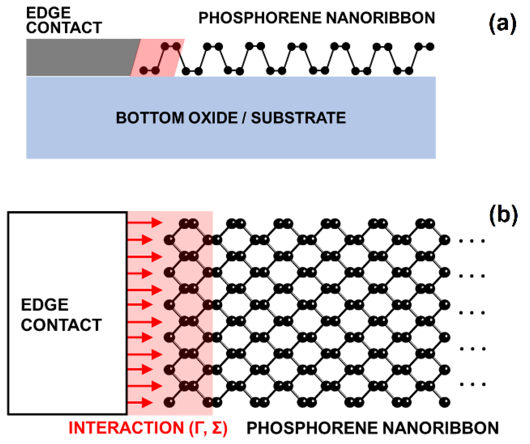
2. Methods
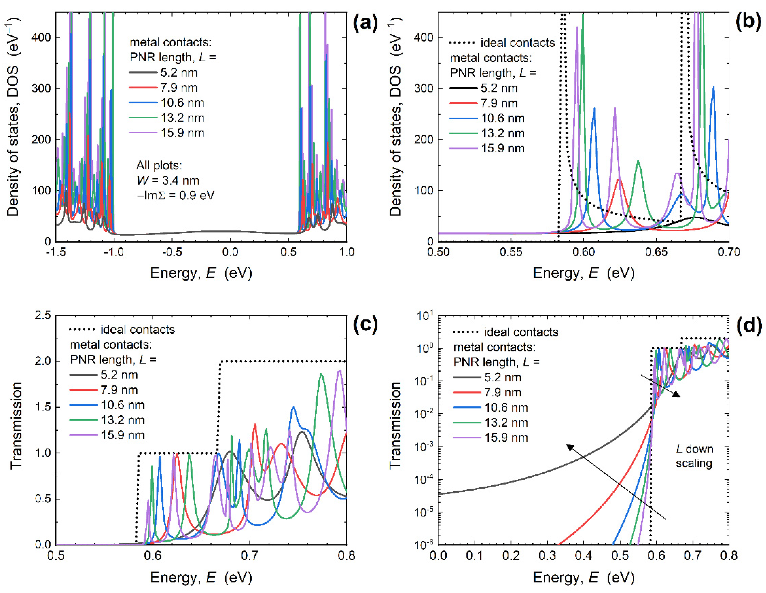
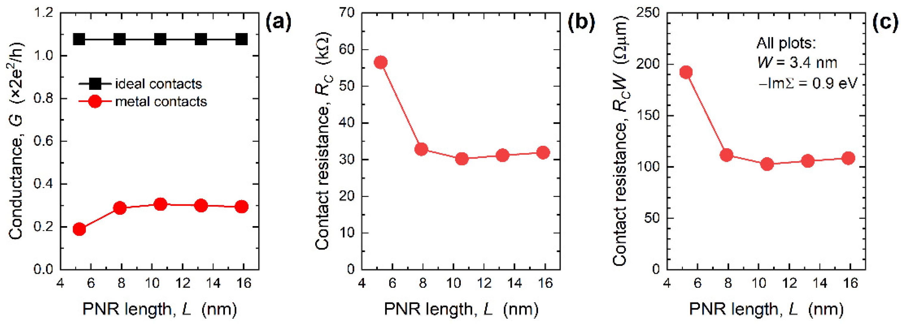
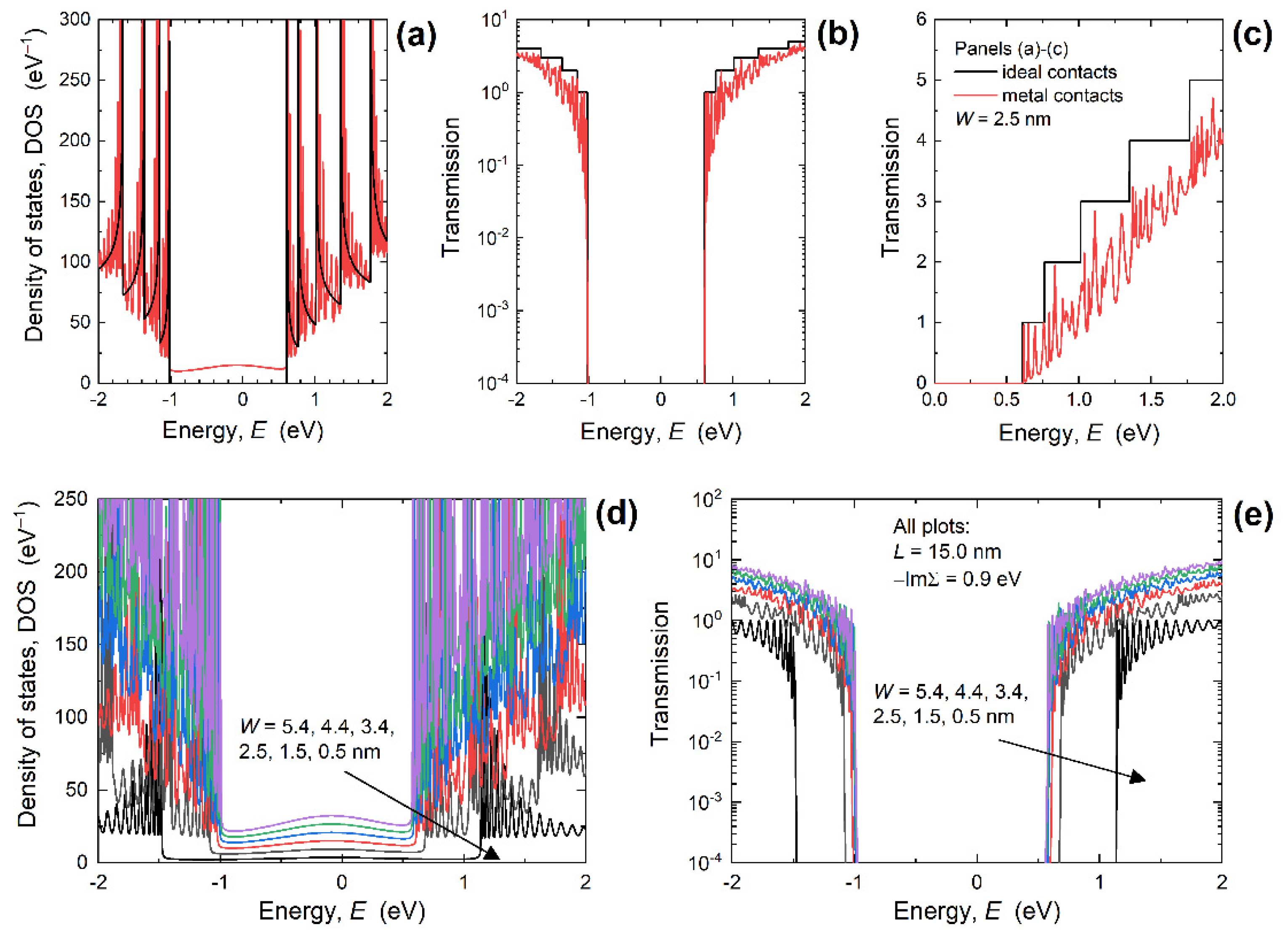
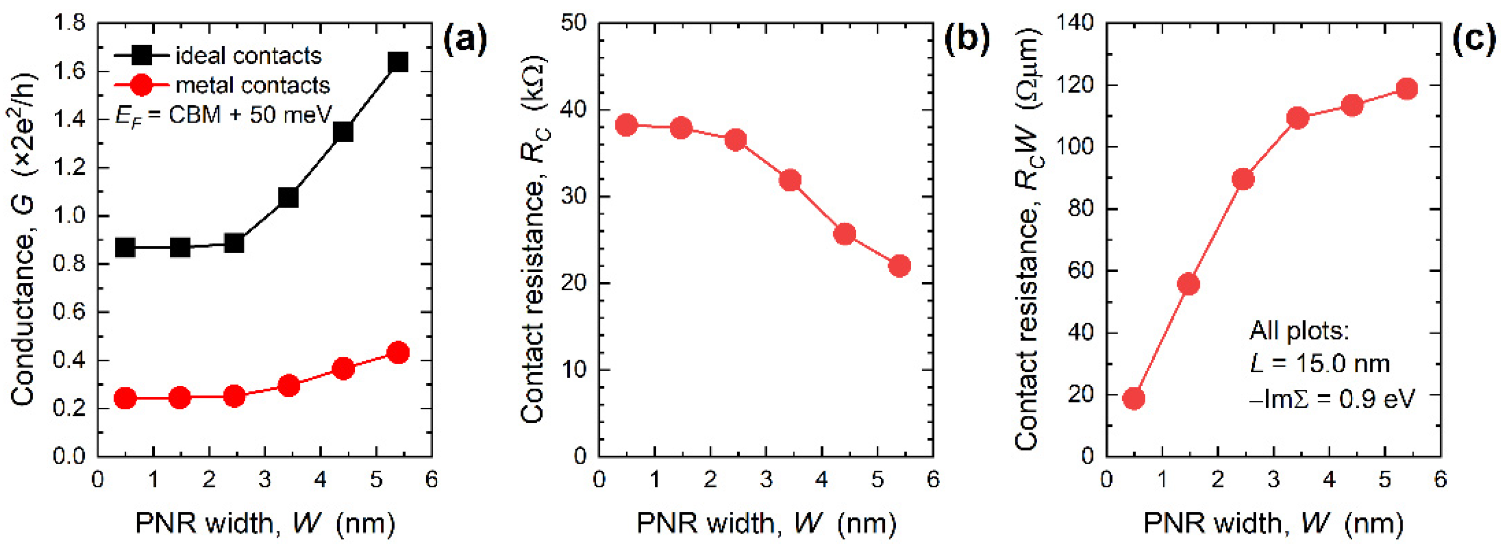
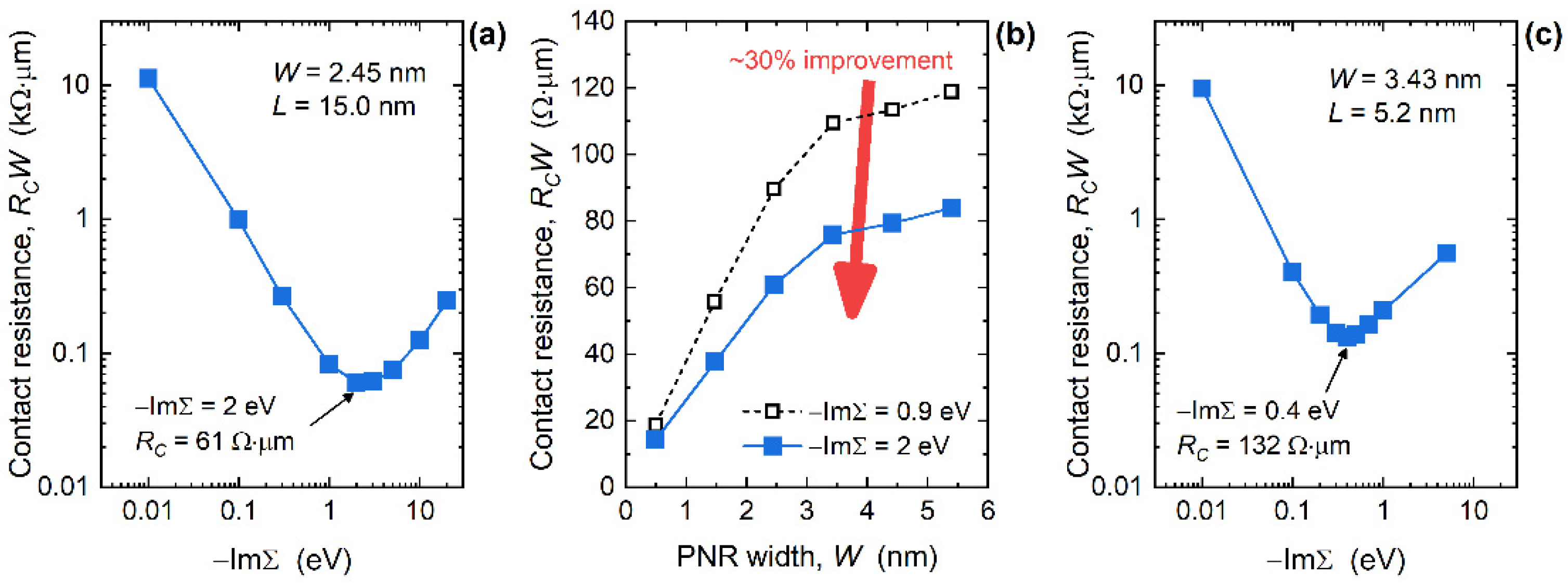
3. Results and Discussion
4. Conclusions
Supplementary Materials
Author Contributions
Funding
Institutional Review Board Statement
Informed Consent Statement
Data Availability Statement
Conflicts of Interest
References
- Fiori, G.; Bonaccorso, F.; Iannaccone, G.; Palacios, T.; Neumaier, D.; Seabaugh, A.; Banerjee, S.K.; Colombo, L. Electronics Based on Two-Dimensional Materials. Nat. Nanotechnol. 2014, 9, 768–779. [Google Scholar] [CrossRef] [PubMed]
- Briggs, N.; Subramanian, S.; Lin, Z.; Li, X.; Zhang, X.; Zhang, K.; Xiao, K.; Geohegan, D.; Wallace, R.; Chen, L.-Q.; et al. A Roadmap for Electronic Grade 2D Materials. 2D Mater. 2019, 6, 022001. [Google Scholar] [CrossRef]
- Pizzi, G.; Gibertini, M.; Dib, E.; Marzari, N.; Iannaccone, G.; Fiori, G. Performance of Arsenene and Antimonene Double-Gate MOSFETs from First Principles. Nat. Commun. 2016, 7, 12585. [Google Scholar] [CrossRef] [PubMed] [Green Version]
- Klinkert, C.; Szabó, Á.; Stieger, C.; Campi, D.; Marzari, N.; Luisier, M. 2-D Materials for Ultrascaled Field-Effect Transistors: One Hundred Candidates under the Ab Initio Microscope. ACS Nano 2020, 14, 8605–8615. [Google Scholar] [CrossRef] [PubMed]
- Afzalian, A. Ab Initio Perspective of Ultra-Scaled CMOS from 2D-Material Fundamentals to Dynamically Doped Transistors. NPJ 2D Mater. Appl. 2021, 5, 5. [Google Scholar] [CrossRef]
- Liu, H.; Neal, A.T.; Zhu, Z.; Luo, Z.; Xu, X.; Tománek, D.; Ye, P.D. Phosphorene: An Unexplored 2D Semiconductor with a High Hole Mobility. ACS Nano 2014, 8, 4033–4041. [Google Scholar] [CrossRef] [Green Version]
- Das, S.; Demarteau, M.; Roelofs, A. Ambipolar Phosphorene Field Effect Transistor. ACS Nano 2014, 8, 11730–11738. [Google Scholar] [CrossRef]
- Li, L.; Yu, Y.; Ye, G.J.; Ge, Q.; Ou, X.; Wu, H.; Feng, D.; Chen, X.H.; Zhang, Y. Black Phosphorus Field-Effect Transistors. Nat. Nanotechnol. 2014, 9, 372–377. [Google Scholar] [CrossRef] [Green Version]
- Haratipour, N.; Robbins, M.C.; Koester, S.J. Black Phosphorus P-MOSFETs with 7-nm HfO2 Gate Dielectric and Low Contact Resistance. IEEE Electron Device Lett. 2015, 36, 411–413. [Google Scholar] [CrossRef]
- Cao, X.; Guo, J. Simulation of Phosphorene Field-Effect Transistor at the Scaling Limit. IEEE Trans. Electron Devices 2015, 62, 659–665. [Google Scholar] [CrossRef]
- Afzalian, A.; Pourtois, G. ATOMOS: An ATomistic MOdelling Solver for Dissipative DFT Transport in Ultra-Scaled HfS2 and Black Phosphorus MOSFETs. In Proceedings of the 2019 International Conference on Simulation of Semiconductor Processes and Devices (SISPAD), Udine, Italy, 4–6 September 2019; pp. 1–4. [Google Scholar]
- Guo, H.; Lu, N.; Dai, J.; Wu, X.; Zeng, X.C. Phosphorene Nanoribbons, Phosphorus Nanotubes, and van Der Waals Multilayers. J. Phys. Chem. C 2014, 118, 14051–14059. [Google Scholar] [CrossRef] [Green Version]
- Taghizadeh Sisakht, E.; Zare, M.H.; Fazileh, F. Scaling Laws of Band Gaps of Phosphorene Nanoribbons: A Tight-Binding Calculation. Phys. Rev. B 2015, 91, 085409. [Google Scholar] [CrossRef] [Green Version]
- Poljak, M.; Suligoj, T. Immunity of Electronic and Transport Properties of Phosphorene Nanoribbons to Edge Defects. Nano Res. 2016, 9, 1723–1734. [Google Scholar] [CrossRef]
- Poljak, M.; Matić, M. Quantum Transport Simulations of Phosphorene Nanoribbon MOSFETs: Effects of Metal Contacts, Ballisticity and Series Resistance. In Proceedings of the 2020 International Conference on Simulation of Semiconductor Processes and Devices (SISPAD), Kobe, Japan, 23 September–6 October 2020; pp. 371–374. [Google Scholar]
- Poljak, M.; Matić, M. Bandstructure and Size-Scaling Effects in the Performance of Monolayer Black Phosphorus Nanodevices. Materials 2022, 15, 243. [Google Scholar] [CrossRef] [PubMed]
- Watts, M.C.; Picco, L.; Russell-Pavier, F.S.; Cullen, P.L.; Miller, T.S.; Bartuś, S.P.; Payton, O.D.; Skipper, N.T.; Tileli, V.; Howard, C.A. Production of Phosphorene Nanoribbons. Nature 2019, 568, 216–220. [Google Scholar] [CrossRef]
- Zhang, W.; Enriquez, H.; Tong, Y.; Mayne, A.J.; Bendounan, A.; Smogunov, A.; Dappe, Y.J.; Kara, A.; Dujardin, G.; Oughaddou, H. Flat Epitaxial Quasi-1D Phosphorene Chains. Nat. Commun. 2021, 12, 5160. [Google Scholar] [CrossRef]
- Du, Y.; Liu, H.; Deng, Y.; Ye, P.D. Device Perspective for Black Phosphorus Field-Effect Transistors: Contact Resistance, Ambipolar Behavior, and Scaling. ACS Nano 2014, 8, 10035–10042. [Google Scholar] [CrossRef] [PubMed] [Green Version]
- Li, X.; Yu, Z.; Xiong, X.; Li, T.; Gao, T.; Wang, R.; Huang, R.; Wu, Y. High-Speed Black Phosphorus Field-Effect Transistors Approaching Ballistic Limit. Sci. Adv. 2019, 5, eaau3194. [Google Scholar] [CrossRef] [Green Version]
- Telesio, F.; le Gal, G.; Serrano-Ruiz, M.; Prescimone, F.; Toffanin, S.; Peruzzini, M.; Heun, S. Ohmic Contact Engineering in Few–Layer Black Phosphorus: Approaching the Quantum Limit. Nanotechnology 2020, 31, 334002. [Google Scholar] [CrossRef]
- Haratipour, N.; Namgung, S.; Grassi, R.; Low, T.; Oh, S.; Koester, S.J. High-Performance Black Phosphorus MOSFETs Using Crystal Orientation Control and Contact Engineering. IEEE Electron Device Lett. 2017, 38, 685–688. [Google Scholar] [CrossRef]
- Poljak, M.; Matić, M.; Zeljko, A. Minimum Contact Resistance in Monoelemental 2D Material Nanodevices with Edge-Contacts. IEEE Electron Device Lett. 2021, 42, 1240–1243. [Google Scholar] [CrossRef]
- Wang, L.; Meric, I.; Huang, P.Y.; Gao, Q.; Gao, Y.; Tran, H.; Taniguchi, T.; Watanabe, K.; Campos, L.M.; Muller, D.A.; et al. One-Dimensional Electrical Contact to a Two-Dimensional Material. Science 2013, 342, 614–617. [Google Scholar] [CrossRef] [PubMed] [Green Version]
- Jain, A.; Szabó, Á.; Parzefall, M.; Bonvin, E.; Taniguchi, T.; Watanabe, K.; Bharadwaj, P.; Luisier, M.; Novotny, L. One-Dimensional Edge Contacts to a Monolayer Semiconductor. Nano Lett. 2019, 19, 6914–6923. [Google Scholar] [CrossRef] [PubMed] [Green Version]
- Rudenko, A.N.; Katsnelson, M.I. Quasiparticle Band Structure and Tight-Binding Model for Single- and Bilayer Black Phosphorus. Phys. Rev. B 2014, 89, 201408. [Google Scholar] [CrossRef] [Green Version]
- Datta, S. Quantum Transport: Atom to Transistor, 2nd ed.; Cambridge University Press: New York, NY, USA, 2005; ISBN 0-521-63145-9. [Google Scholar]
- Pourfath, M. The Non-Equilibrium Green’s Function Method for Nanoscale Device Simulation; Computational Microelectronics; Springer: Wien, Austria, 2014; ISBN 978-3-7091-1799-6. [Google Scholar]
- Poljak, M.; Glavan, M.; Kuzmić, S. Accelerating Simulation of Nanodevices Based on 2D Materials by Hybrid CPU-GPU Parallel Computing. In Proceedings of the 2019 42nd International Convention on Information and Communication Technology, Electronics and Microelectronics (MIPRO), Opatija, Croatia, 20–24 May 2019; pp. 51–56. [Google Scholar]
- Poljak, M. Electron Mobility in Defective Nanoribbons of Monoelemental 2D Materials. IEEE Electron Device Lett. 2020, 41, 151–154. [Google Scholar] [CrossRef]
- Poljak, M.; Matić, M. Metallization-Induced Quantum Limits of Contact Resistance in Graphene Nanoribbons with One-Dimensional Contacts. Materials 2021, 14, 3670. [Google Scholar] [CrossRef]
- Datta, S. Nanoscale Device Modeling: The Green’s Function Method. Superlattices Microstruct. 2000, 28, 253–278. [Google Scholar] [CrossRef]
- Liang, G.; Neophytou, N.; Lundstrom, M.S.; Nikonov, D.E. Contact Effects in Graphene Nanoribbon Transistors. Nano Lett. 2008, 8, 1819–1824. [Google Scholar] [CrossRef]
- Liang, G.; Neophytou, N.; Lundstrom, M.S.; Nikonov, D.E. Ballistic Graphene Nanoribbon Metal-Oxide-Semiconductor Field-Effect Transistors: A Full Real-Space Quantum Transport Simulation. J. Appl. Phys. 2007, 102, 054307. [Google Scholar] [CrossRef] [Green Version]
- Meersha, A.; Variar, H.B.; Bhardwaj, K.; Mishra, A.; Raghavan, S.; Bhat, N.; Shrivastava, M. Record Low Metal—(CVD) Graphene Contact Resistance Using Atomic Orbital Overlap Engineering. In Proceedings of the 2016 IEEE International Electron Devices Meeting (IEDM), San Francisco, CA, USA, 3–7 December 2016; pp. 119–122. [Google Scholar]
- Nemec, N.; Tománek, D.; Cuniberti, G. Modeling Extended Contacts for Nanotube and Graphene Devices. Phys. Rev. B 2008, 77, 125420. [Google Scholar] [CrossRef] [Green Version]
- Fediai, A.; Ryndyk, D.A.; Cuniberti, G. The Modular Approach Enables a Fully Ab Initio Simulation of the Contacts between 3D and 2D Materials. J. Phys. Condens. Matter 2016, 28, 395303. [Google Scholar] [CrossRef] [PubMed] [Green Version]
- Fediai, A.; Ryndyk, D.A.; Seifert, G.; Mothes, S.; Claus, M.; Schröter, M.; Cuniberti, G. Towards an Optimal Contact Metal for CNTFETs. Nanoscale 2016, 8, 10240–10251. [Google Scholar] [CrossRef] [PubMed] [Green Version]
- Pan, Y.; Wang, Y.; Ye, M.; Quhe, R.; Zhong, H.; Song, Z.; Peng, X.; Yu, D.; Yang, J.; Shi, J.; et al. Monolayer Phosphorene–Metal Contacts. Chem. Mater. 2016, 28, 2100–2109. [Google Scholar] [CrossRef]
- Li, J.; Sun, X.; Xu, C.; Zhang, X.; Pan, Y.; Ye, M.; Song, Z.; Quhe, R.; Wang, Y.; Zhang, H.; et al. Electrical Contacts in Monolayer Blue Phosphorene Devices. Nano Res. 2018, 11, 1834–1849. [Google Scholar] [CrossRef]
- Zhang, X.; Pan, Y.; Ye, M.; Quhe, R.; Wang, Y.; Guo, Y.; Zhang, H.; Dan, Y.; Song, Z.; Li, J.; et al. Three-Layer Phosphorene-Metal Interfaces. Nano Res. 2018, 11, 707–721. [Google Scholar] [CrossRef]


Publisher’s Note: MDPI stays neutral with regard to jurisdictional claims in published maps and institutional affiliations. |
© 2022 by the authors. Licensee MDPI, Basel, Switzerland. This article is an open access article distributed under the terms and conditions of the Creative Commons Attribution (CC BY) license (https://creativecommons.org/licenses/by/4.0/).
Share and Cite
Poljak, M.; Matić, M.; Župančić, T.; Zeljko, A. Lower Limits of Contact Resistance in Phosphorene Nanodevices with Edge Contacts. Nanomaterials 2022, 12, 656. https://doi.org/10.3390/nano12040656
Poljak M, Matić M, Župančić T, Zeljko A. Lower Limits of Contact Resistance in Phosphorene Nanodevices with Edge Contacts. Nanomaterials. 2022; 12(4):656. https://doi.org/10.3390/nano12040656
Chicago/Turabian StylePoljak, Mirko, Mislav Matić, Tin Župančić, and Ante Zeljko. 2022. "Lower Limits of Contact Resistance in Phosphorene Nanodevices with Edge Contacts" Nanomaterials 12, no. 4: 656. https://doi.org/10.3390/nano12040656
APA StylePoljak, M., Matić, M., Župančić, T., & Zeljko, A. (2022). Lower Limits of Contact Resistance in Phosphorene Nanodevices with Edge Contacts. Nanomaterials, 12(4), 656. https://doi.org/10.3390/nano12040656