
Role of Junctionless Mode in Improving the Photosensitivity of Sub-10 nm Carbon Nanotube/Nanoribbon Field-Effect Phototransistors: Quantum Simulation, Performance Assessment, and Comparison

 ,
, 
 , ,
, , 

Abstract
:1. Introduction
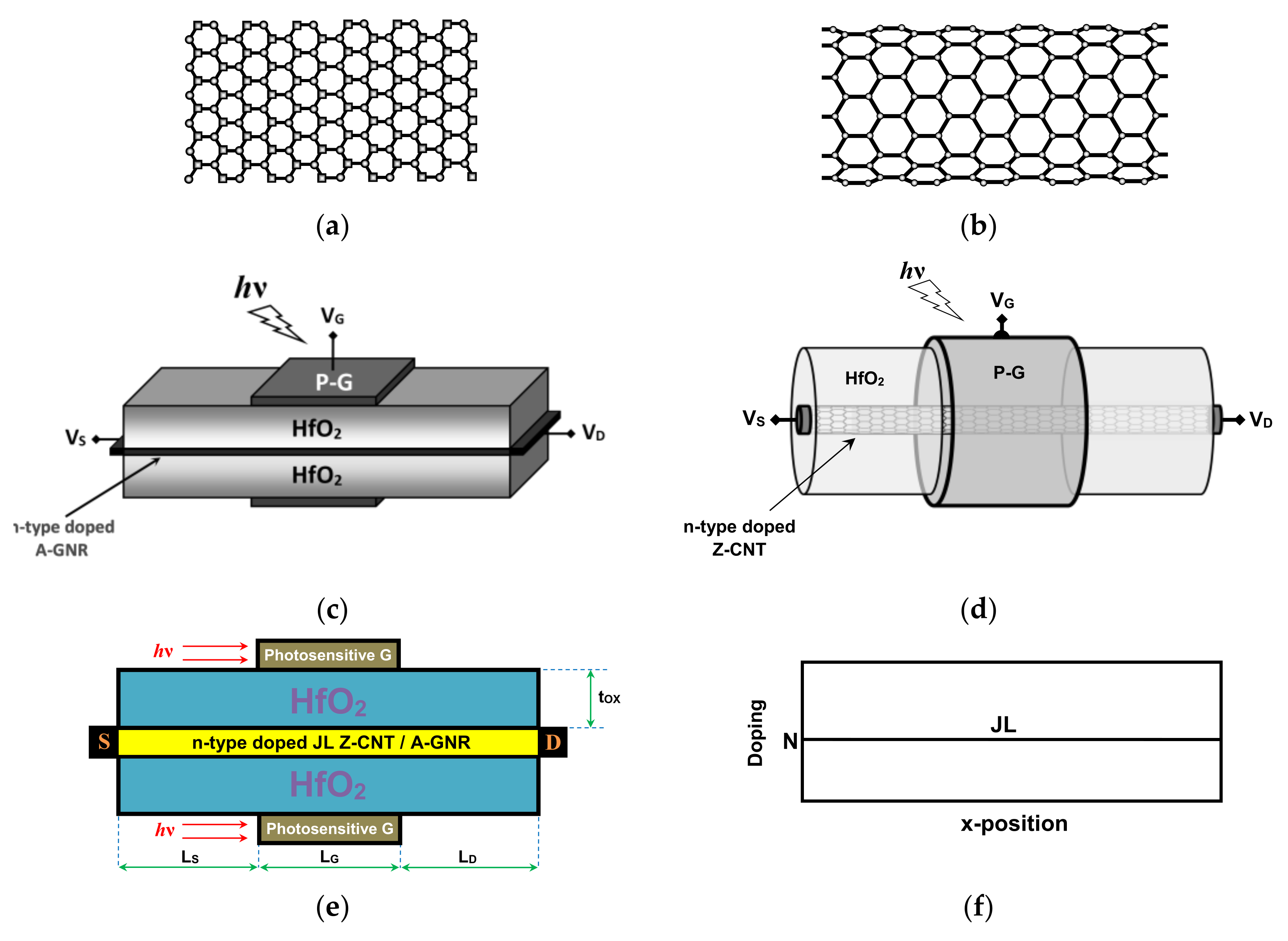
2. Device Structure
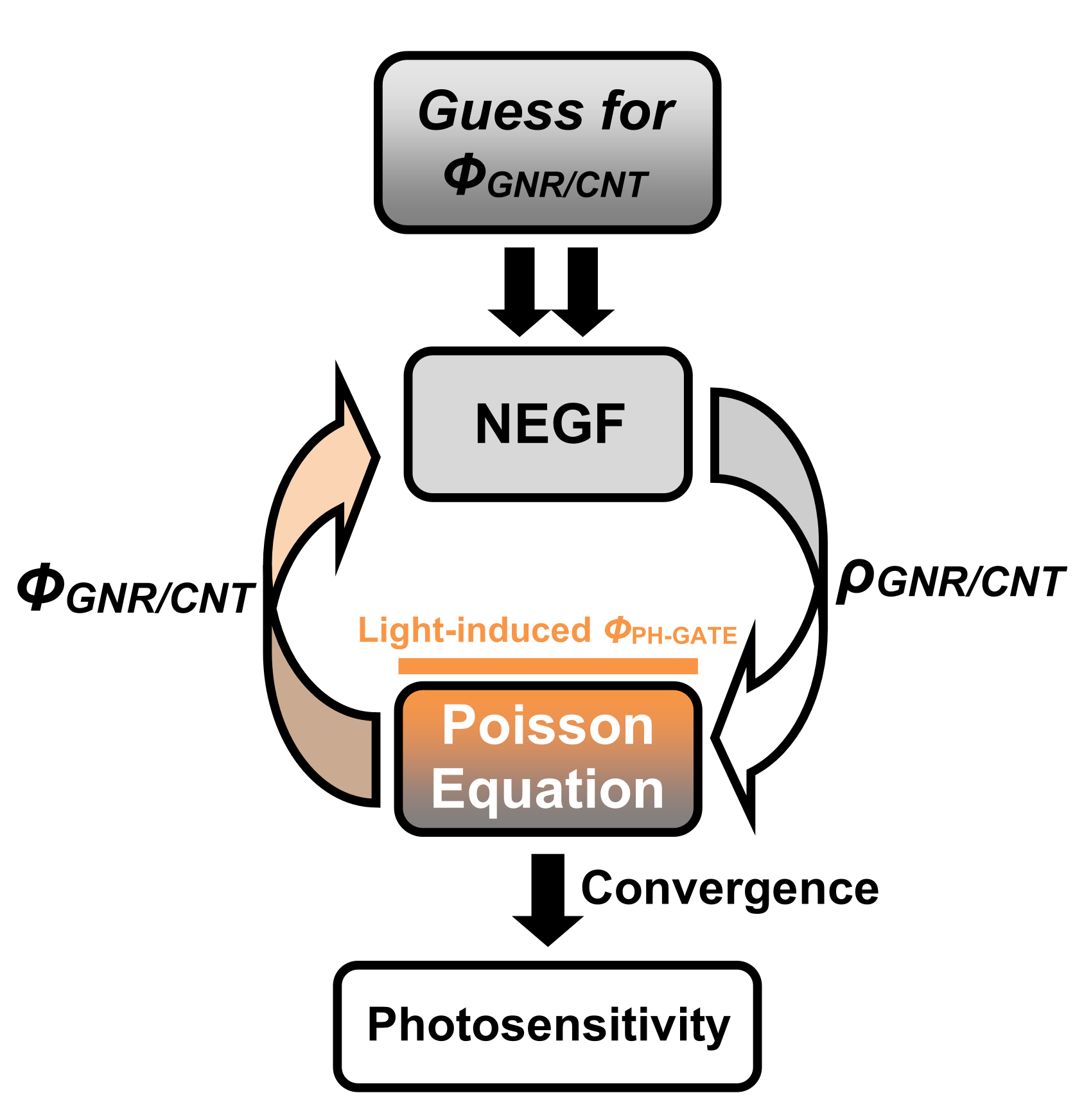
3. Quantum Simulation Approach
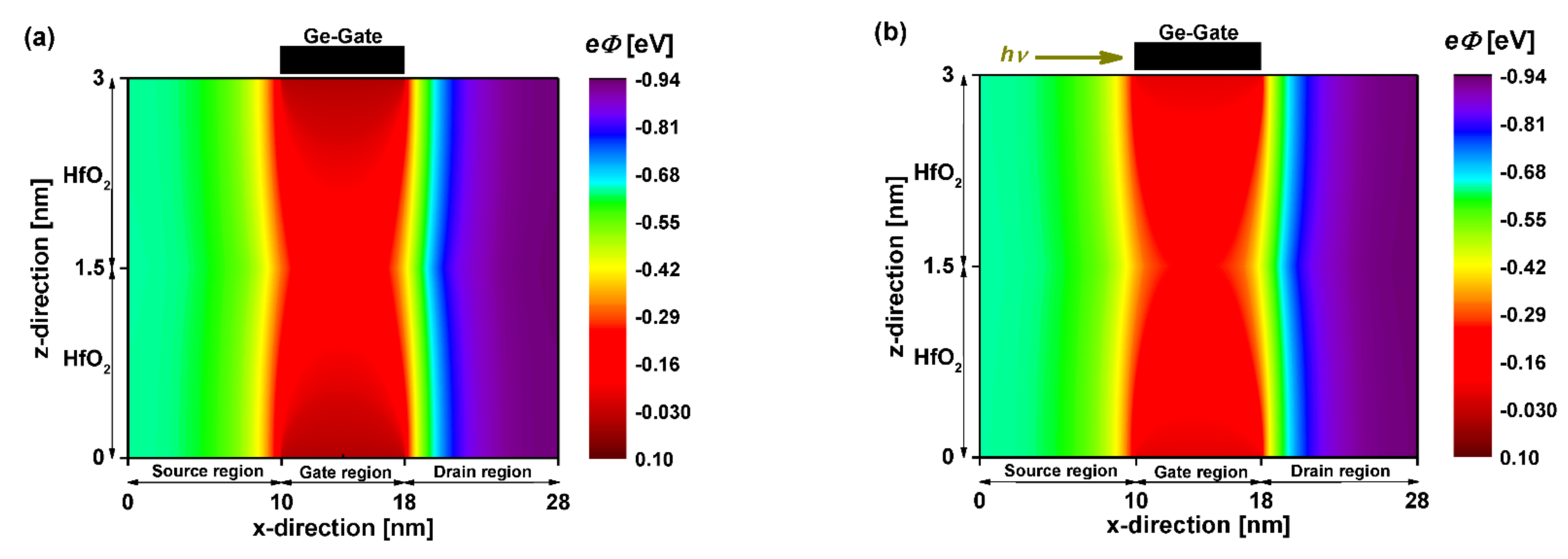
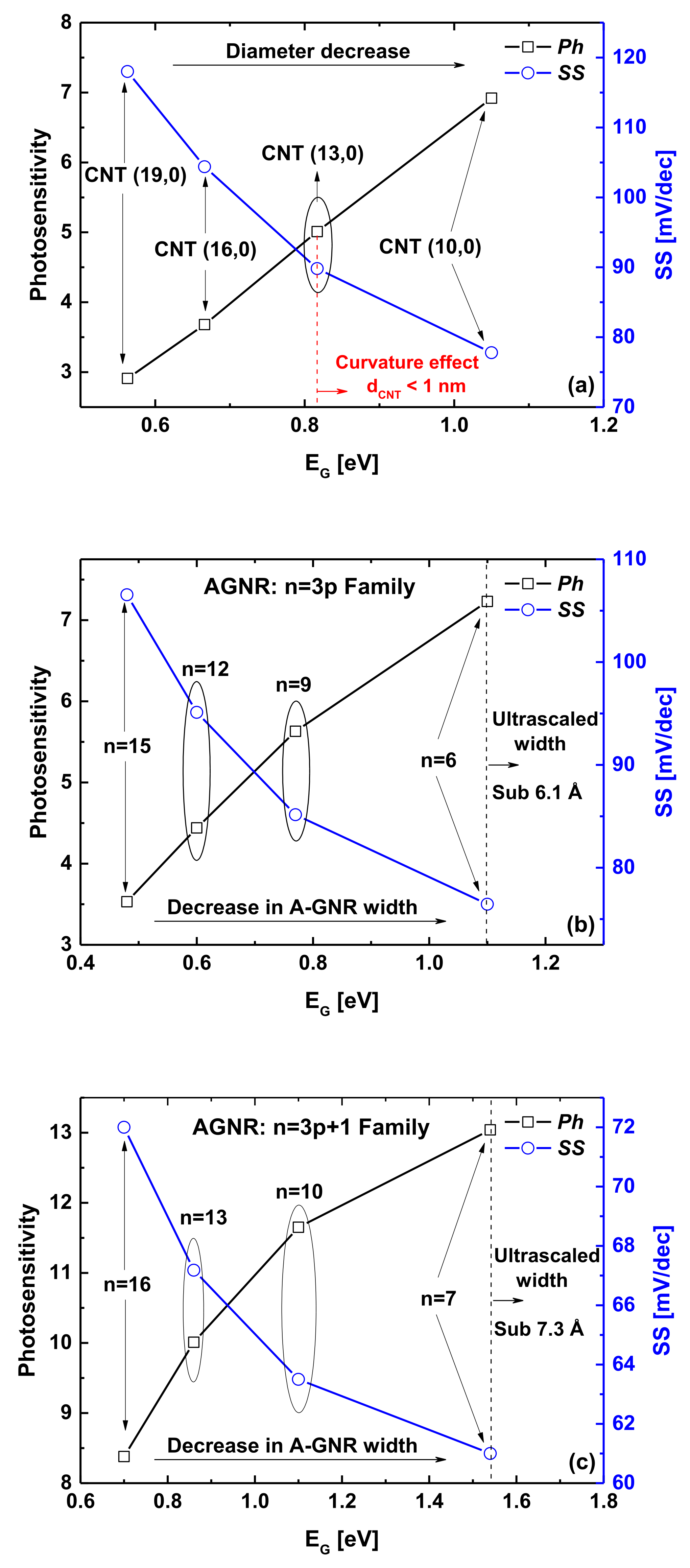
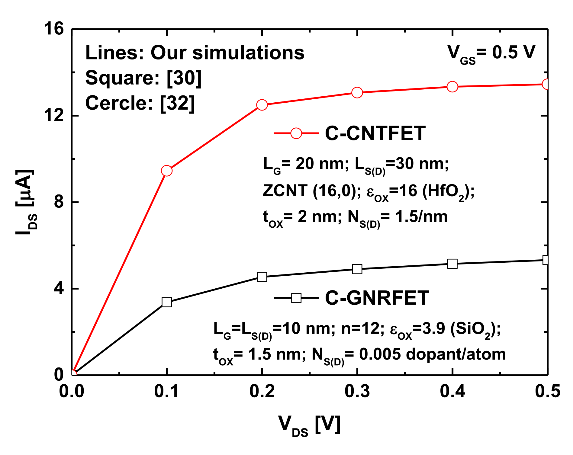
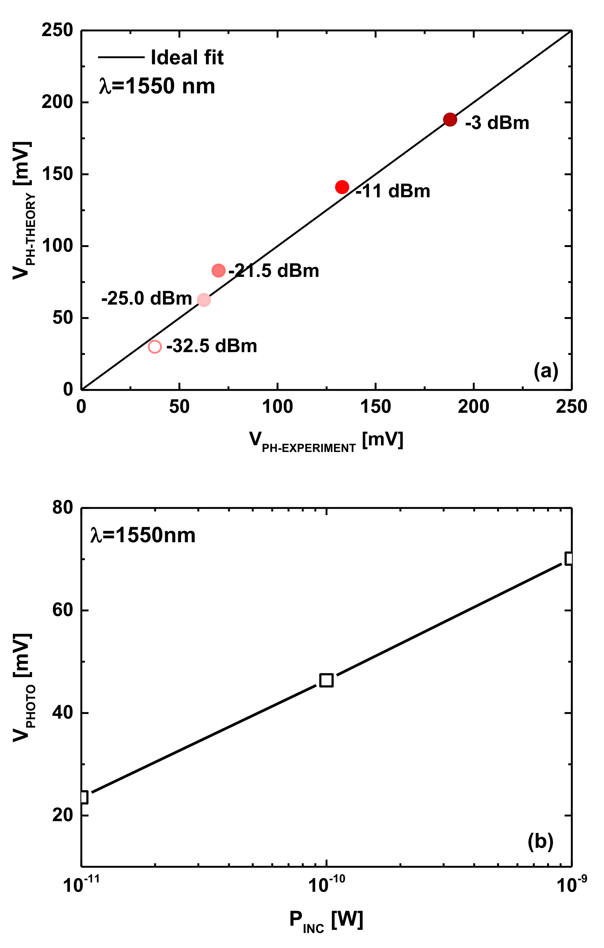
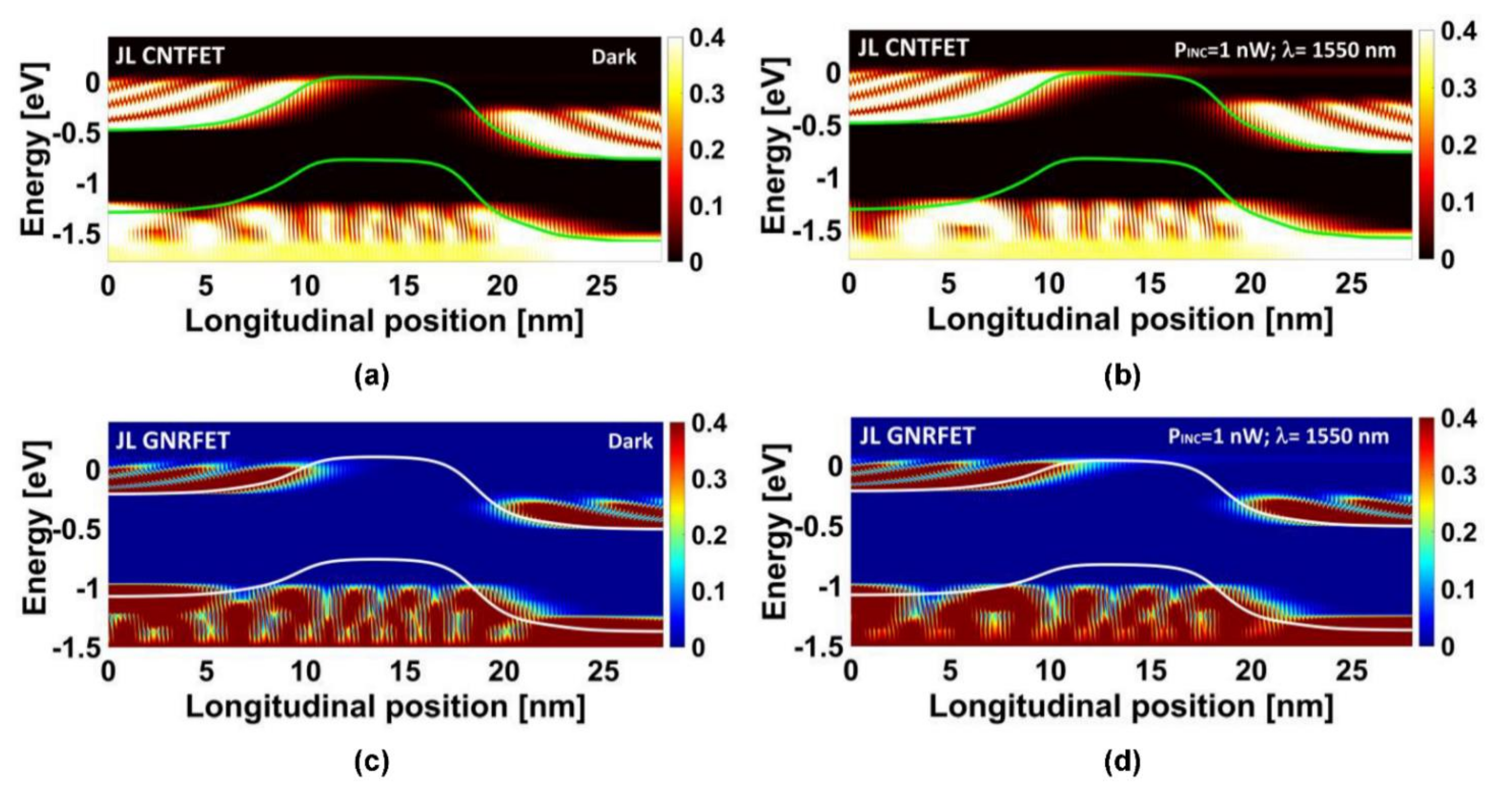
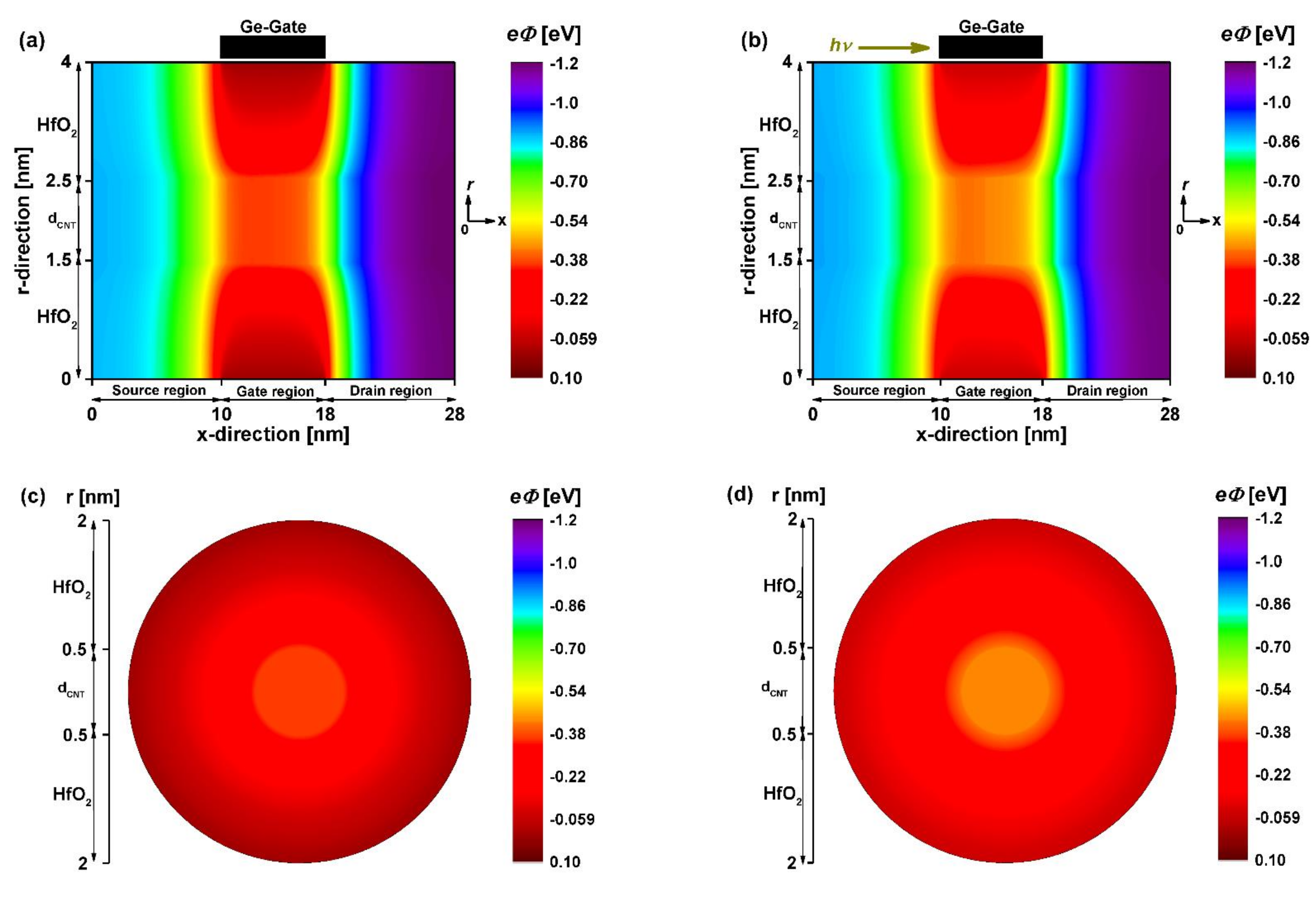
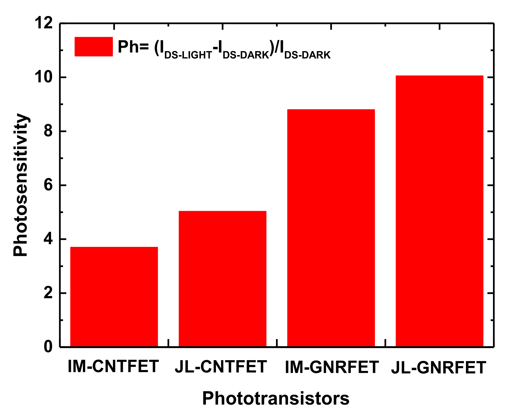
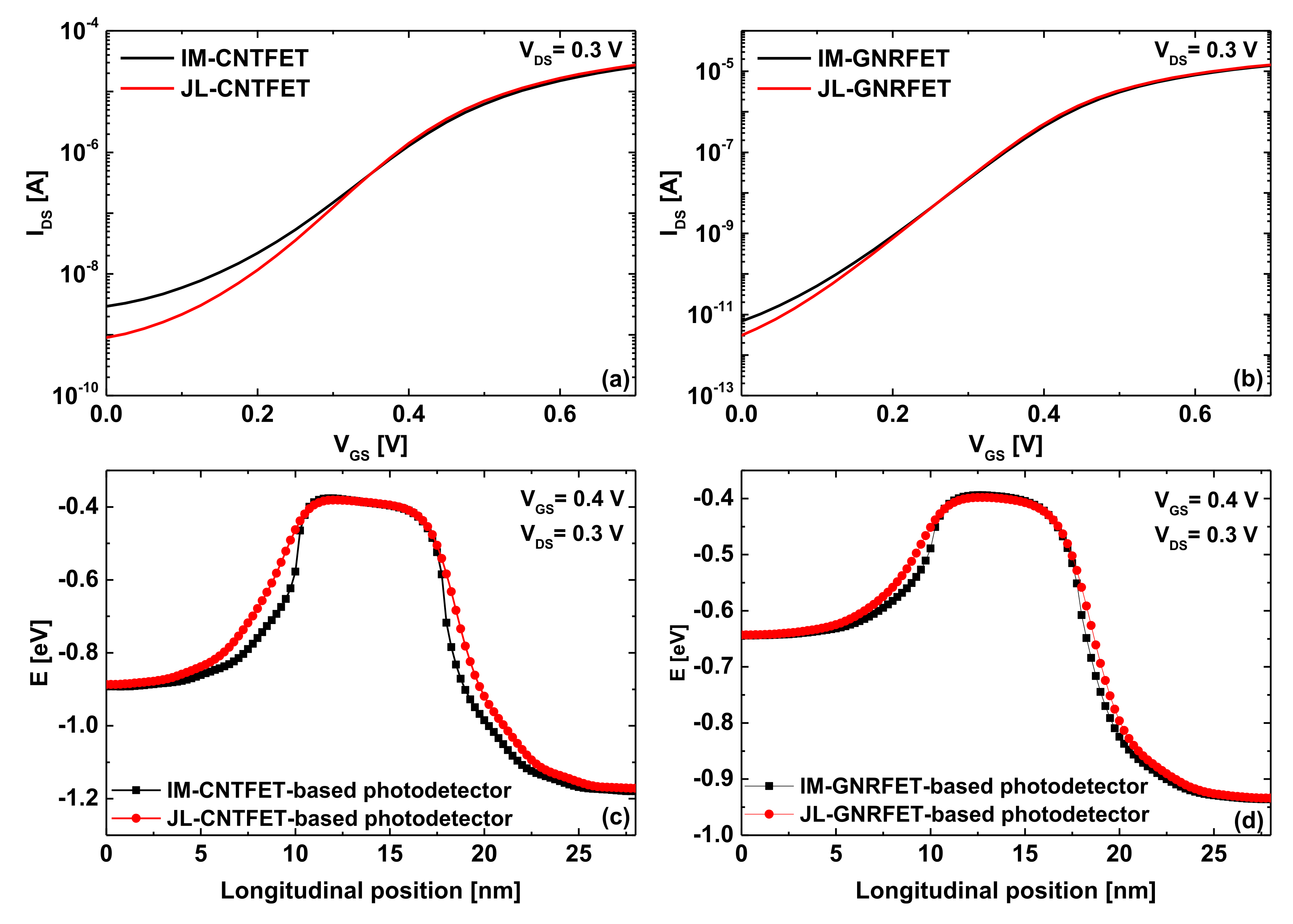
4. Results and Discussion
5. Conclusions
Author Contributions
Funding
Institutional Review Board Statement
Informed Consent Statement
Data Availability Statement
Acknowledgments
Conflicts of Interest
References
- DJariwala, D.; Sangwan, V.K.; Lauhon, L.J.; Marks, T.J.; Hersam, M.C. Carbon nanomaterials for electronics, optoelectronics, photovoltaics, and sensing. Chem. Soc. Rev. 2012, 42, 2824–2860. [Google Scholar] [CrossRef] [PubMed] [Green Version]
- Avouris, P.; Freitag, M.; Perebeinos, V. Carbon-nanotube photonics and optoelectronics. Nat. Photonics 2008, 2, 341–350. [Google Scholar] [CrossRef]
- Garg, R.; Dutta, N.K.; Choudhury, N.R. Work Function Engineering of Graphene. Nanomaterials 2014, 4, 267–300. [Google Scholar] [CrossRef] [PubMed] [Green Version]
- Du, J.; Pei, S.; Ma, L.; Cheng, H.-M. 25th Anniversary Article: Carbon Nanotube- and Graphene-Based Transparent Conductive Films for Optoelectronic Devices. Adv. Mater. 2014, 26, 1958–1991. [Google Scholar] [CrossRef]
- Avouris, P.; Chen, J. Nanotube electronics and optoelectronics. Mater. Today 2006, 9, 46–54. [Google Scholar] [CrossRef]
- Marcus, M.S.; Simmons, J.M.; Castellini, O.M.; Hamers, R.; Eriksson, M.A. Photogating carbon nanotube transistors. J. Appl. Phys. 2006, 100, 084306. [Google Scholar] [CrossRef] [Green Version]
- Chen, H.Z.; Xi, N.; Lai, K.W.C.; Chen, L.L.; Yang, R.; Song, B. Gate dependent photo-responses of carbon nanotube field effect phototransistors. Nanotechnology 2012, 23, 385203. [Google Scholar] [CrossRef]
- Salimian, S.; Araghi, M.E.A. Study of the preparation and spectral response of stacked graphene nanoribbon-carbon nanotube-based phototransistors. Carbon 2016, 107, 754–764. [Google Scholar] [CrossRef]
- Chang, H.; Wu, H. Graphene-Based Nanomaterials: Synthesis, Properties, and Optical and Optoelectronic Applications. Adv. Funct. Mater. 2012, 23, 1984–1997. [Google Scholar] [CrossRef]
- Tamersit, K. Energy-Efficient Carbon Nanotube Field-Effect Phototransistors: Quantum Simulation, Device Physics, and Photosensitivity Analysis. IEEE Sens. J. 2021, 22, 288–296. [Google Scholar] [CrossRef]
- Castro Neto, A.H.; Guinea, F.; Peres, N.M.R.; Novoselov, K.S.; Geim, A.K. The electronic properties of graphene. Rev. Mod. Phys. 2009, 81, 109–162. [Google Scholar] [CrossRef] [Green Version]
- Baughman, R.H.; Zakhidov, A.A.; de Heer, W.A. Carbon Nanotubes—The Route Toward Applications. Science 2002, 297, 787–792. [Google Scholar] [CrossRef] [PubMed] [Green Version]
- Polat, E.O.; Mercier, G.; Nikitskiy, I.; Puma, E.; Galan, T.; Gupta, S.; Montagut, M.; Piqueras, J.J.; Bouwens, M.; Durduran, T.; et al. Flexible graphene photodetectors for wearable fitness monitoring. Sci. Adv. 2019, 5, eaaw7846. [Google Scholar] [CrossRef] [PubMed] [Green Version]
- Voronin, K.V.; Ermolaev, G.A.; Stebunov, Y.V.; Arsenin, A.V.; Bylinkin, A.N.; Jensen, B.B.E.; Jørgensen, B.; Volkov, V.S. Photogating in graphene field-effect phototransistors: Theory and observations. In Proceedings of Inter-National Congress on Graphene, 2d Materials and Applications (2D MATERIALS 2019); AIP Publishing: Woodbury, New York, NY, USA; 2021; Volume 2359, p. 020034. [Google Scholar] [CrossRef]
- Vaquero, D.; Clericò, V.; Salvador-Sánchez, J.; Díaz, E.; Domínguez-Adame, F.; Chico, L.; Meziani, Y.M.; Diez, E.; Quereda, J. Fast response photogating in monolayer MoS2 phototransistors. Nanoscale 2021, 13, 16156–16163. [Google Scholar] [CrossRef]
- Fang, H.; Hu, W. Photogating in Low Dimensional Photodetectors. Adv. Sci. 2017, 4, 1700323. [Google Scholar] [CrossRef] [PubMed]
- Going, R.W.; Loo, J.; Liu, T.-J.K.; Wu, M.C. Germanium Gate PhotoMOSFET Integrated to Silicon Photonics. IEEE J. Sel. Top. Quantum Electron. 2013, 20, 1–7. [Google Scholar] [CrossRef]
- Guo, J.; Alam, M.A.; Yoon, Y. Theoretical investigation on photoconductivity of single intrinsic carbon nanotubes. Appl. Phys. Lett. 2006, 88, 133111. [Google Scholar] [CrossRef]
- Gao, Q.; Guo, J. Quantum mechanical simulation of graphene photodetectors. J. Appl. Phys. 2012, 112, 084316. [Google Scholar] [CrossRef]
- Joshi, S.; Dubey, P.K.; Kaushik, B.K. A Transition Metal Dichalcogenide Tunnel FET-Based Waveguide-Integrated Photodetector Using Ge for Near-Infrared Detection. IEEE Sens. J. 2019, 19, 9187–9193. [Google Scholar] [CrossRef]
- Joshi, S.; Dubey, P.K.; Kaushik, B.K. Photosensor Based on Split Gate TMD TFET Using Photogating Effect for Visible Light Detection. IEEE Sens. J. 2020, 20, 6346–6353. [Google Scholar] [CrossRef]
- Kadri, A.; Djeffal, F.; Ferhati, H.; Menacer, F.; Dibi, Z. Performance analysis of a new graphene based-phototransistor for ultra-sensitive infrared sensing applications. Optik 2018, 176, 24–31. [Google Scholar] [CrossRef]
- Farah, S.; Ferhati, H.; Dibi, Z.; Djeffal, F. Performance analysis of broadband Mid-IR graphene-phototransistor using strained black phosphorus sensing gate: DFT-NEGF investigation. Superlattices Microstruct. 2022, 107187. [Google Scholar] [CrossRef]
- Kadri, A.; Ferhati, H.; Djeffal, F. Giant responsivity of a new optically controlled graphene UV-phototransistor using graded band-gap ZnMgO gate. Sens. Actuators A Phys. 2021, 325, 112701. [Google Scholar] [CrossRef]
- Fiori, G.; Bonaccorso, F.; Iannaccone, G.; Palacios, T.; Neumaier, D.; Seabaugh, A.; Banerjee, S.K.; Colombo, L. Electronics based on two-dimensional materials. Nat. Nanotechnol. 2014, 9, 768–779. [Google Scholar] [CrossRef] [PubMed]
- Tamersit, K. A new ultra-scaled graphene nanoribbon junctionless tunneling field-effect transistor: Proposal, quantum simulation, and analysis. J. Comput. Electron. 2019, 19, 170–176. [Google Scholar] [CrossRef]
- Tamersit, K.; Kouzou, A.; Bourouba, H.; Kennel, R.; Abdelrahem, M. Synergy of electrostatic and chemical doping to improve the performance of junctionless carbon nanotube tunneling field-effect transistors: Ultrascaling, energy-efficiency, and high switching performance. Nanomaterials 2022, 12, 462. [Google Scholar] [CrossRef]
- Hammam, A.; Schmidt, M.E.; Muruganathan, M.; Suzuki, S.; Mizuta, H. Sub-10 nm graphene nano-ribbon tunnel field-effect transistor. Carbon 2018, 126, 588–593. [Google Scholar] [CrossRef]
- Colinge, J.P.; Lee, C.W.; Akhavan, N.D.; Yan, R.; Ferain, I.; Razavi, P.; Kranti, A.; Yu, R. Junctionless Transistors: Physics and Properties. In Semiconductor-On-Insulator Materials for Nanoelec-tronics Applications; Springer: Berlin/Heidelberg, Germany, 2011; pp. 187–200. [Google Scholar] [CrossRef]
- Zhao, P.; Guo, J. Modeling edge effects in graphene nanoribbon field-effect transistors with real and mode space methods. J. Appl. Phys. 2009, 105, 034503. [Google Scholar] [CrossRef] [Green Version]
- Yousefi, R.; Shabani, M.O.; Arjmandi, M.; Ghoreishi, S. A computational study on electrical characteristics of a novel band-to-band tunneling graphene nanoribbon FET. Superlattices Microstruct. 2013, 60, 169–178. [Google Scholar] [CrossRef]
- Koswatta, S.O.; Hasan, S.; Lundstrom, M.S.; Anantram, M.P.; Nikonov, D. Nonequilibrium Green’s Function Treatment of Phonon Scattering in Carbon-Nanotube Transistors. IEEE Trans. Electron Devices 2007, 54, 2339–2351. [Google Scholar] [CrossRef] [Green Version]
- Tamersit, K. An ultra-sensitive gas nanosensor based on asymmetric dual-gate graphene nanoribbon field-effect transistor: Proposal and investigation. J. Comput. Electron. 2019, 18, 846–855. [Google Scholar] [CrossRef]
- Son, Y.-W.; Cohen, M.L.; Louie, S.G. Energy Gaps in Graphene Nanoribbons. Phys. Rev. Lett. 2006, 97, 216803. [Google Scholar] [CrossRef] [PubMed] [Green Version]
- Guo, J.; Datta, S.; Lundstrom, M.; Anantam, M.P. Toward Multiscale Modeling of Carbon Nanotube Transistors. Int. J. Multiscale Comput. Eng. 2004, 2, 257–276. [Google Scholar] [CrossRef]
- Ghoreishi, S.S.; Vadizadeh, M.; Yousefi, R.; Afzalian, A. Low-Power Ultradeep-Submicrometer Junctionless Carbon Nanotube Field-Effect Diode. IEEE Trans. Electron Devices 2021, 69, 400–405. [Google Scholar] [CrossRef]
- Tamersit, K. Improving the performance of a junctionless carbon nanotube field-effect transistor using a split-gate. AEU-Int. J. Electron. Commun. 2020, 115, 153035. [Google Scholar] [CrossRef]
- Colinge, J.-P.; Lee, C.-W.; Afzalian, A.; Akhavan, N.D.; Yan, R.; Ferain, I.; Razavi, P.; O’Neill, B.; Blake, A.; White, M.; et al. Nanowire transistors without junctions. Nat. Nanotechnol. 2010, 5, 225–229. [Google Scholar] [CrossRef]
- Tamersit, K. A computational study of short-channel effects in double-gate junctionless graphene nanoribbon field-effect transistors. J. Comput. Electron. 2019, 18, 1214–1221. [Google Scholar] [CrossRef]
- Tamersit, K. Sub-10 nm junctionless carbon nanotube field-effect transistors with improved performance. AEU-Int. J. Electron. Commun. 2020, 124, 153354. [Google Scholar] [CrossRef]
- Liu, M.; Wang, H.; Tang, Q.; Zhao, X.; Tong, Y.; Liu, Y. Ultrathin Air-Stable n-Type Organic Phototransistor Array for Conformal Optoelectronics. Sci. Rep. 2018, 8, 16612. [Google Scholar] [CrossRef]
- Tamersit, K.; Djeffal, F. Double-Gate Graphene Nanoribbon Field-Effect Transistor for DNA and Gas Sensing Applications: Simulation Study and Sensitivity Analysis. IEEE Sens. J. 2016, 16, 4180–4191. [Google Scholar] [CrossRef]
- Tamersit, K. Performance enhancement of an ultra-scaled double-gate graphene nanoribbon tunnel field-effect transistor using channel doping engineering: Quantum simulation study. AEU-Int. J. Electron. Commun. 2020, 122, 153287. [Google Scholar] [CrossRef]
- Datta, S. Nanoscale device modeling: The Green’s function method. Superlattices Microstruct. 2000, 28, 253–278. [Google Scholar] [CrossRef]
- Datta, S. Electronic Transport in Mesoscopic Systems; Cambridge University Press: Cambridge, UK, 1997. [Google Scholar]
- Tamersit, K.; Djeffal, F. A computationally efficient hybrid approach based on artificial neural networks and the wavelet transform for quantum simulations of graphene nanoribbon FETs. J. Comput. Electron. 2019, 18, 813–825. [Google Scholar] [CrossRef]
- Moghaddam, S.; Ghoreishi, S.S.; Yousefi, R.; Aderang, H. Quantum simulation of a junctionless carbon nanotube field-effect transistor under torsional strain. Superlattices Microstruct. 2019, 138, 106239. [Google Scholar] [CrossRef]
- Tamersit, K.; Ramezani, Z.; Amiri, I.S. Improved performance of sub-10-nm band-to-band tunneling n-i-n graphene nanoribbon field-effect transistors using underlap engineering: A quantum simulation study. J. Phys. Chem. Solids 2022, 160, 110312. [Google Scholar] [CrossRef]
- Tamersit, K. A novel band-to-band tunneling junctionless carbon nanotube field-effect transistor with lightly doped pocket: Proposal, assessment, and quantum transport analysis. Phys. E Low-Dimens. Syst. Nanostruct. 2021, 128, 114609. [Google Scholar] [CrossRef]
- Dassi, M.; Madan, J.; Pandey, R.; Sharma, R. Chemical modulation of conducting polymer gate electrode work function based double gate Mg2Si TFET for gas sensing applications. J. Mater. Sci. Mater. Electron. 2022, 1–10. [Google Scholar] [CrossRef]
- Mehrad, M.; Zareiee, M. Using Hetro-Structure Window in Nano Scale Junctionless SOI MOSFET for High Electrical Performance. ECS J. Solid State Sci. Technol. 2021, 10, 111005. [Google Scholar] [CrossRef]
- Tamersit, K. New nanoscale band-to-band tunneling junctionless GNRFETs: Potential high-performance devices for the ultrascaled regime. J. Comput. Electron. 2021, 20, 1147–1156. [Google Scholar] [CrossRef]
- Banadaki, Y.M.; Srivastava, A. Investigation of the width-dependent static characteristics of graphene nanoribbon field effect transistors using non-parabolic quantum-based model. Solid-State Electron. 2015, 111, 80–90. [Google Scholar] [CrossRef]
- Banadaki, Y.M.; Srivastava, A. Scaling Effects on Static Metrics and Switching Attributes of Graphene Nanoribbon FET for Emerging Technology. IEEE Trans. Emerg. Top. Comput. 2015, 3, 458–469. [Google Scholar] [CrossRef]
- Tamersit, K.; Kotti, M.; Fakhfakh, M. A new pressure microsensor based on dual-gate graphene field-effect transistor with a vertically movable top-gate: Proposal, analysis, and optimization. AEU-Int. J. Electron. Commun. 2020, 124, 153346. [Google Scholar] [CrossRef]
- Tamersit, K. Improved performance of nanoscale junctionless carbon nanotube tunneling FETs using dual-material source gate design: A quantum simulation study. AEU-Int. J. Electron. Commun. 2020, 127, 153491. [Google Scholar] [CrossRef]
- Anvarifard, M.K.; Ramezani, Z.; Amiri, I.S.; Tamersit, K.; Nejad, A.M. Profound analysis on sensing performance of Nanogap SiGe source DM-TFET biosensor. J. Mater. Sci. Mater. Electron. 2020, 31, 22699–22712. [Google Scholar] [CrossRef]
- Tamersit, K. Boosting the performance of an ultrascaled carbon nanotube junctionless tunnel field-effect transistor using an ungated region: NEGF simulation. J. Comput. Electron. 2019, 18, 1222–1228. [Google Scholar] [CrossRef]
- Jooq, M.K.Q.; Moaiyeri, M.H.; Tamersit, K. Ultra-Compact Ternary Logic Gates Based on Negative Capacitance Carbon Nanotube FETs. IEEE Trans. Circuits Syst. II Express Briefs 2020, 68, 2162–2166. [Google Scholar] [CrossRef]
- Tamersit, K. Improved Switching Performance of Nanoscale p-i-n Carbon Nanotube Tunneling Field-Effect Transistors Using Metal-Ferroelectric-Metal Gating Approach. ECS J. Solid State Sci. Technol. 2021, 10, 031004. [Google Scholar] [CrossRef]
- Tamersit, K.; Jooq, M.K.Q.; Moaiyeri, M.H. Analog/RF performance assessment of ferroelectric junctionless carbon nanotube FETs: A quantum simulation study. Phys. E Low-Dimens. Syst. Nanostruct. 2021, 134, 114915. [Google Scholar] [CrossRef]
- Behbahani, F.; Jooq, M.K.Q.; Moaiyeri, M.H.; Tamersit, K. Leveraging Negative Capacitance CNTFETs for Image Processing: An Ultra-Efficient Ternary Image Edge Detection Hardware. IEEE Trans. Circuits Syst. I Regul. Pap. 2021, 68, 5108–5119. [Google Scholar] [CrossRef]
- Salahuddin, S.; Datta, S. Use of Negative Capacitance to Provide Voltage Amplification for Low Power Nanoscale Devices. Nano Lett. 2007, 8, 405–410. [Google Scholar] [CrossRef]
- Tu, L.; Wang, X.; Wang, J.; Meng, X.; Chu, J. Ferroelectric Negative Capacitance Field Effect Transistor. Adv. Electron. Mater. 2018, 4, 1800231. [Google Scholar] [CrossRef]
- Wong, J.C.; Salahuddin, S. Negative Capacitance Transistors. Proc. IEEE 2019, 107, 49–62. [Google Scholar] [CrossRef]


| Parameter | Symbol | DG JL GNRFET | GAA JL CNTFET | Unit |
|---|---|---|---|---|
| Dimmer number | n | 13 | 13 | - |
| Bandgap | EG | ~0.86 | ~0.81 | eV |
| Width/diameter | WGNR/dCNT | ~1.47 | ~1 | nm |
| Sensitive gate length | LG | 8 | 8 | nm |
| S/D length | LS(D) | 10 | 10 | nm |
| S/C/D doping | NS/C/D | 0.56 | 1.5 | nm−1 |
| Oxide thickness | tOX | 1.5 | 1.5 | nm |
| Oxide dielectric constant | εOX | 16 | 16 | - |
| Temperature | T | 300 | 300 | K |
| Light wavelength | λ | 1550 | 1550 | nm |
| Drain-to-source voltage | VDS | 0.3 | 0.3 | V |
Publisher’s Note: MDPI stays neutral with regard to jurisdictional claims in published maps and institutional affiliations. |
© 2022 by the authors. Licensee MDPI, Basel, Switzerland. This article is an open access article distributed under the terms and conditions of the Creative Commons Attribution (CC BY) license (https://creativecommons.org/licenses/by/4.0/).
Share and Cite
Tamersit, K.; Madan, J.; Kouzou, A.; Pandey, R.; Kennel, R.; Abdelrahem, M. Role of Junctionless Mode in Improving the Photosensitivity of Sub-10 nm Carbon Nanotube/Nanoribbon Field-Effect Phototransistors: Quantum Simulation, Performance Assessment, and Comparison. Nanomaterials 2022, 12, 1639. https://doi.org/10.3390/nano12101639
Tamersit K, Madan J, Kouzou A, Pandey R, Kennel R, Abdelrahem M. Role of Junctionless Mode in Improving the Photosensitivity of Sub-10 nm Carbon Nanotube/Nanoribbon Field-Effect Phototransistors: Quantum Simulation, Performance Assessment, and Comparison. Nanomaterials. 2022; 12(10):1639. https://doi.org/10.3390/nano12101639
Chicago/Turabian StyleTamersit, Khalil, Jaya Madan, Abdellah Kouzou, Rahul Pandey, Ralph Kennel, and Mohamed Abdelrahem. 2022. "Role of Junctionless Mode in Improving the Photosensitivity of Sub-10 nm Carbon Nanotube/Nanoribbon Field-Effect Phototransistors: Quantum Simulation, Performance Assessment, and Comparison" Nanomaterials 12, no. 10: 1639. https://doi.org/10.3390/nano12101639
APA StyleTamersit, K., Madan, J., Kouzou, A., Pandey, R., Kennel, R., & Abdelrahem, M. (2022). Role of Junctionless Mode in Improving the Photosensitivity of Sub-10 nm Carbon Nanotube/Nanoribbon Field-Effect Phototransistors: Quantum Simulation, Performance Assessment, and Comparison. Nanomaterials, 12(10), 1639. https://doi.org/10.3390/nano12101639