Article

Solution-Processed SnO2 Quantum Dots for the Electron Transport Layer of Flexible and Printed Perovskite Solar Cells

by
Muhammad Salman Kiani
1,
Zhandos T. Sadirkhanov
1,
Alibek G. Kakimov
1,
Hryhorii P. Parkhomenko
1,
Annie Ng
2 and
Askhat N. Jumabekov
1,*
1
Department of Physics, Nazarbayev University, Nur-Sultan 010000, Kazakhstan
2
Department of Electrical and Computer Engineering, Nazarbayev University, Nur-Sultan 010000, Kazakhstan
*
Author to whom correspondence should be addressed.
Nanomaterials 2022, 12(15), 2615; https://doi.org/10.3390/nano12152615
Submission received: 10 June 2022 / Revised: 14 July 2022 / Accepted: 25 July 2022 / Published: 29 July 2022
(This article belongs to the Special Issue Nanomaterials for Solar Energy Conversion and Storage)

Abstract

:
Flexible and printed perovskite solar cells (PSCs) fabricated on lightweight plastic substrates have many excellent potential applications in emerging new technologies including wearable and portable electronics, the internet of things, smart buildings, etc. To fabricate flexible and printed PSCs, all of the functional layers of devices should be processed at low temperatures. Tin oxide is one of the best metal oxide materials to employ as the electron transport layer (ETL) in PSCs. Herein, the synthesis and application of SnO2 quantum dots (QDs) to prepare the ETL of flexible and printed PSCs are demonstrated. SnO2 QDs are synthesized via a solvothermal method and processed to obtain aqueous and printable ETL ink solutions with different QD concentrations. PSCs are fabricated using a slot-die coating method on flexible plastic substrates. The solar cell performance and spectral response of the obtained devices are characterized using a solar simulator and an external quantum efficiency measurement system. The ETLs prepared using 2 wt% SnO2 QD inks are found to produce devices with a high average power conversion efficiency (PCE) along with a 10% PCE for a champion device. The results obtained in this work provide the research community with a method to prepare fully solution-processed SnO2 QD-based inks that are suitable for the deposition of SnO2 ETLs for flexible and printed PSCs.

1. Introduction

With the tremendous improvement in the power conversion efficiency (PCE) up to 25.7% in the matter of a decade, hybrid perovskite solar cells (PSCs) made their mark in the electronic industry [1,2,3,4]. Even though some challenges such as device stability still need to be addressed, there has been a growing interest in scaling up the PSC fabrication process. Most high-efficiency PSCs are currently manufactured using the spin-coating method because of the better control over the film thickness, quality, and reproducibility of the device functional layers as well as the possibility of applying different spin-coating techniques such as dynamic spinning, hot-casting, anti-solvent annealing, gas and vacuum-quenching, etc. [5,6]. In comparison to other solution-processed techniques, spin-coating is an easy method to fabricate high-quality perovskite films [7]. One of the main limitations of the spin-coating method is its non-scalability [8]. Hence, various scalable methods including screen printing, blade coating, inkjet printing, and slot-die coating have been developed to fabricate PSCs [9,10,11,12,13,14]. The printing methods provide an appealing strategy for large-scale and high-throughput fabrication and can help to accelerate the commercialization of PSC technology [15,16,17,18].
Slot-die coating is one of the more appealing scalable coating methods due to its ability to produce solution-processed thin films with a high uniformity across large areas, its ability to coat thin films at a higher speed, its lesser material waste, and its ability to be integrated into both sheet-to-sheet (S2S) and roll-to-roll coating (R2R) systems. This affords the fabrication of PSCs on both rigid and flexible substrates [19,20]. Flexible and printed PSCs are of high interest due to their lightweight nature, portability, and low-manufacturing cost, along with the possibility of integrating them into other technologies, which promises many potential lucrative applications of this technology in wearable electronics, the internet of things (IoT), smart buildings, the automobile industry, etc. Flexible devices can be achieved by replacing traditional glass substrates with plastic substrates, such as polyethylene terephthalate (PET) or polyethylene naphthalate (PEN), with a thin layer of transparent conducting oxide (TCO). The TCO layer is typically made of indium-doped tin oxide (ITO). However, other alternatives also exist [21,22,23].
To successfully fabricate flexible PSCs, the three main semiconducting device functional layers, which are the electron transport layer (ETL, n-type), the perovskite photo-absorber layer (i-type), and the hole transport layer (HTL, p-type), must be processed at temperatures below the glass transition temperature of the employed plastic substrates (usually < 150 °C) [24,25,26]. The ETL is responsible for the extraction of electrons from the perovskite photo-absorber layer and then for their efficient transportation to the TCO layer. Mostly, metal oxides such as ZnO, TiO2, or SnO2 are used as ETL [27,28]. However, there are other alternatives that can be based on ternary metal oxides and organic materials (e.g., BaSnO3, Zn2SnO4, PEDOT:PSS, PEDOT:PSS:MoS2, etc.) [29,30]. By covering the surface of TCO, ETL prevents the direct contact between the TCO and perovskite layers [31]. The selection of an efficient ETL requires a material with a good optical transmittance (in the visible range), a high electron mobility, a low production cost, and the energy levels (conduction and valence band energies) that form a good type-2 junction with the energy levels of the chosen perovskite material [32]. Among all the candidates, SnO2 stands out as one of the best candidates for ETL due to its wide optical band gap (3.6–4.0 eV), deep conduction band, better transparency, high electron mobility (~240 cm2 V−1 s−1), long carrier diffusion length, excellent chemical stability, and ease of low-temperature preparation (via solution processing) [33,34,35,36]. Due to its solution processibility, SnO2 can be printed and bring advantages such as a low production cost, flexibility, easy scalability, and additive manufacturing processes within reach [37,38,39].
In 2018, T. Bu et al. reported slot-die coated flexible PSCs with an ETL made of commercially available SnO2 NPs (15% of colloidal dispersion in H2O, Alfa Aesar). The resultant devices, in which a mixed cation and mixed anion perovskite (Cs0.05(FA0.85MA0.15)0.95Pb(I0.85Br0.15)3) are employed as a photoactive layer and Spiro-OMeTAD is employed as an HTL, showed PCE values around 18% [40]. In 2020, Vijayaraghavan et al. reported the use of solution-processed SnO2 quantum dots as an ETL for PSCs. The ETL was prepared in an aqueous medium using DI water, SnCl2·2H2O, and thiourea as precursors. PCE values of around 13.5% have been achieved at an annealing temperature of 180 °C, and the devices are fabricated on glass substrates via the spin-coating method [41]. In 2021, Ashina et al. deposited the SnO2 ETLs using a dip-coating method on glass substrates with a fluorine-doped tin oxide (FTO) layer as the TCO. The authors deposited multiple layers (1–4) of a SnO2 precursor solution and achieved PCE values around 3.2%. The annealing temperature for the ETL was set to 150 °C [1]. While the aforementioned PCE values obtained with the SnO2 ETLs are appreciable, the annealing temperatures used in these studies, however, are still too high from the flexible PSC fabrication perspective. In 2021, Ren et al. reported a fabrication of PSCs on glass/FTO substrates using the blade coating method, in which the ETLs of devices are made of SnO2 QDs with an annealing temperature of 200 °C. The authors achieved devices with PCE values around 21.6%. The obtained devices are fabricated by using a mixed perovskite consisting of FAI:MABr:MACl:PbBr2:PbI2 (molar ratio: 1.1:0.2:0.5:0.2:1.2) in DMF:DMSO solvent and by employing an air-knife for the deposition of the perovskite layer [42]. Using SnO2 QDs instead of NPs provides the advantage of having a thin, dense, and uniform film of ETL. QDs have a wider bandgap (about 4.20 eV) compared to NPs, and this enhances the optical transmittance of the resulting ETL [43]. The main issue that limits the use of SnO2 ETL for flexible devices is its annealing temperature, which has been found > 150 °C, while the typical flexible substrates such as PET and PEN usually have temperature limitations in terms of their structural integrity [40,44,45,46]. One of the possible solutions for this could be the use of already crystalline SnO2 QDs for the solution-processed deposition of SnO2 ETLs. Here, the use of already crystalline SnO2 QDs would not only result in crystalline SnO2 ETLs but would also allow for the avoidance of the high-temperature processing step, which is crucial for devices based on plastic substrates. The low-temperature and solution-processed deposition of SnO2 ETL is advantageous from the perspective of flexible and printed optoelectronics.
In this work, a method to employ SnO2 quantum dots, synthesized via a solvothermal method, to prepare ETLs of flexible PSCs fabricated on PET/ITO substrates is demonstrated. For the synthesis of SnO2 quantum dots, tin chloride and ethanol are used as the solute and solvents, respectively. The obtained quantum dots are crystalline with sizes ~2.4 nm [47]. The obtained SnO2 QDs are used to prepare aqueous inks with different SnO2 QD concentrations to slot-die coat ETLs on PET/ITO substrates with a low annealing temperature. The obtained ETLs on PET/ITO substrates are then used to fabricate flexible and printed PSCs by also using the slot-die coating method. The metallic contacts (gold electrodes) of the devices are deposited using a thermal evaporator and a shadow mask. The solar cell performances of the devices are compared to rule out the best ETL ink composition. A statistical analysis of the device performance parameters is carried out, and the performance of the champion device is discussed. The findings of this study can be useful in the synthesis and use of SnO2 QDs for application in printed and flexible optoelectronics.

2. Materials and Methods

2.1. Materials

Methylammonium iodide (MAI, 99.995%) was purchased from GreatCell Solar. Tin chlo-ride dihydrate (SnCl2·2H2O, 98%), lead iodide (PbI2, 99%), chlorobenzene (CB, 99.80%), 4-tert-Butylpyridine (4tBp, 98%), bis(trifluoromethane)sulfonimide lithium salt (Li-TFSI, 99%), acetonitrile (ACN, 99.80%), methylamine solution (MA, 33 wt% in ab-solute ethanol), and acetone (99.80%) were purchased from Merck. 2,2′,7,7′-Tetrakis-(N,N-di-4-methoxyphenylamino)-9,9′-spirobifluorene (Spiro-MeOTAD, 99.50%) and potassium hydroxide pellets (KOH, 85%) were purchased from Lumtec and ACS reagent, respectively. 2-Propanol (IPA, 99.80%) and ethanol (96.3%) were purchased from a local supplier. Gold (Au, 99.99%) was purchased from Kurt. J. Lesker. All the chemicals were used as received without any treatment.

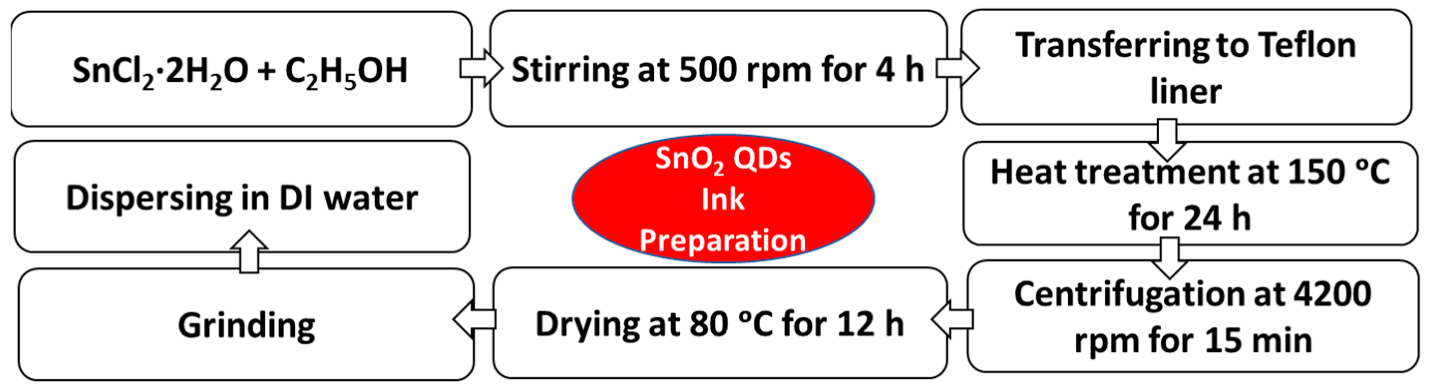
2.2. SnO2 QDs Synthesis

SnO2 QDs were prepared by dissolving 1 mol of SnCl2·2H2O in 10 mL of ethanol in the presence of oxygen. The mixture of precursors was vigorously stirred for 4 h using a magnetic stirrer. The obtained QD solution was then transferred into a 50 mL Teflon liner in a stainless-steel autoclave (Toption). The solvothermal treatment was carried out at 150 °C in an oven for 24 h [48]. After this, the obtained solution was centrifuged to precipitate the SnO2 QDs. The obtained precipitate (SnO2 QDs) was washed consecutively with DI water, acetone, and ethanol. Then, the SnO2 QDs were dried at 80 °C in the oven for 12 h. A flow chart in Figure 1 shows the process for the synthesis of SnO2 QDs to prepare SnO2 QD inks.

2.3. Ink Preparations

The aqueous SnO2 QD inks were prepared using freshly synthesized SnO2 QDs. For this, the dried powder of SnO2 QDs was ground and redispersed in DI water (at different wt%) with the help of 1 M KOH (in water) solution as a pH mediator (see Figure 1). The obtained colloidal solution was then filtered using a 0.45 μm-sized PTFE filter and further diluted with DI water to obtain the final ink solutions, with the concentrations of SnO2 QDs being 1, 1.5, 2, 2.5, and 3 wt%. The perovskite (methylammonium lead iodide, MAPbI3) ink was prepared using PbI2 and MAI as precursors, while MA and ACN were used as solvents. For this, 1 mol of PbI2 and MAI were dissolved in 700 µL of MA by stirring at 70 °C and 460 rpm for 1 h using a hot plate with a magnetic stirrer. Next, 700 µL of ACN was added to the solution and stirred at room temperature for an additional 3 h. The obtained final perovskite ink solution was then filtered using a 0.45 μm-sized PTFE filter and was ready for use. The HTL ink was prepared by simply dissolving 45 mg of Spiro-MeOTAD in 1 mL of CB using a vortex shaker. After 1 h of shaking, 28.8 µL 4tBp and 17.5 µL lithium salt solution (520 mg mL−1 of Li-TFSI in ACN) were added to the Spiro-MeOTAD/CB solution. The final HTL ink solution was then filtered using a 0.45 μm-sized PTFE filter for further use.

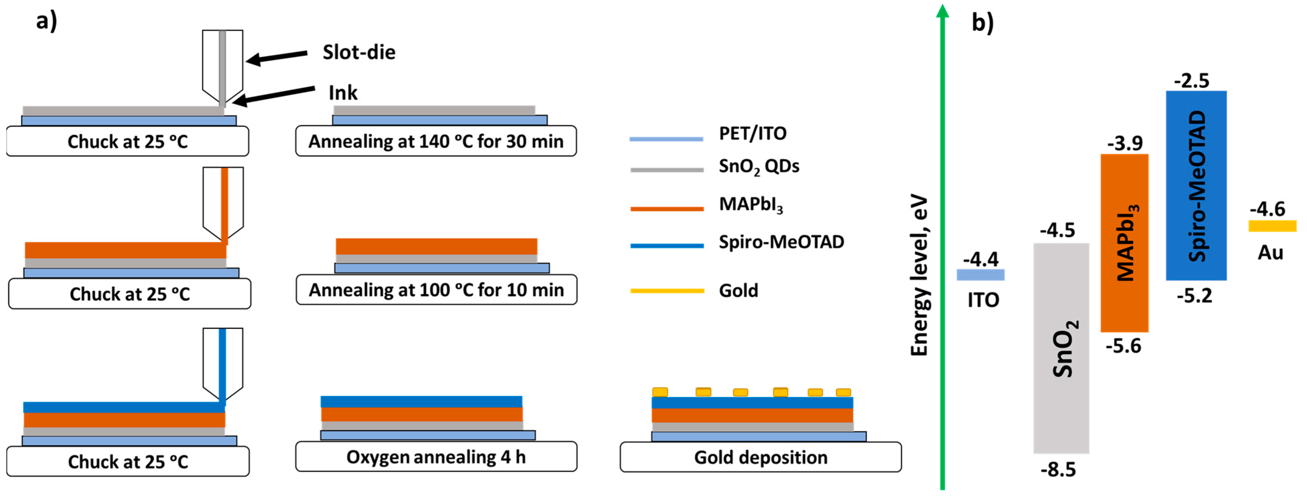
2.4. Device Fabrication

For the fabrication of flexible and printed PSCs, a freshly cleaned PET/ITO substrate was placed onto the chuck of a slot-die coater (VectorSC, FOM Technologies, Copenhagen, Denmark) and fixed using vacuum suction to keep the substrate perfectly flat on the surface of the chuck. The PET/ITO substrates were cleaned by (1) washing them consecutively in DI detergent water, clean DI water, acetone, and IPA for 10 min in each media using an ultrasonic bath, (2) drying them with the flow of compressed air, and (3) subjecting them to UV-Ozone treatment for 10 min. The SnO2 QDs inks were printed on the PET/ITO substrates using a clean slot-die head. Then, the substrates were annealed in the oven at 140 °C for 30 min. This step is necessary to remove the remaining water from the ETL film prior to the deposition of the perovskite layer on top of it. Once the substrates were cooled down to room temperature, they were placed onto the chuck of the slot-die coater again, and the perovskite ink was printed on top of the ETL using a clean slot-die head. Then, the substrates were annealed again in the oven at 100 °C for 10 min to crystallize the perovskite layer. Next, the HTL ink was printed on top of the perovskite layer using a clean slot-die head. All of the device functional layers were printed in an ambient environment at room temperature (17 °C) and a relative humidity of 20–24%. After depositing all the functional layers, the substrates were left in the atmosphere of oxygen at room temperature for 4 h (oxygen annealing). This step helps to enhance the hole transporting properties of the Spiro-MeOTAD HTL. Finally, the 80 nm-thick Au electrodes were deposited using a vacuum thermal evaporator (Mini SPECTROS, Kurt J. Lesker, USA) and a shadow mask. Overall, the devices have the following structure: PET/ITO/SnO2/MAPbI3/Spiro-MeOTAD/Au. Figure 2 represents a schematic diagram of the device fabrication process and an energy level diagram for the fabricated PSCs [49,50]. The reference devices without ETL were also fabricated using the exact same steps as those in the regular devices (with ETL), except for the ETL deposition step, which was omitted. Hence, the reference devices have the following structure: PET/ITO/MAPbI3/Spiro-MeOTAD/Au.

2.5. Characterization

A transmission electron microscope (TEM, JEOL JEM - 1400 Plus, Tokyo, Japan) was used to estimate the particle size and crystallinity of the obtained SnO2 QDs. An X-ray diffractometer (XRD, SmartLab Rigaku, Austin, TX, USA) was used to examine the crystal structure of the SnO2 QDs (using Cu Kα = 1.5418 Å). A scanning electron microscope (SEM, Zeiss Crossbeam 540, Oberkochen, Germany) was used to obtain the cross-section images of the fabricated devices and to study the morphology of the prepared ETLs. The optical transmittance of the samples was measured using a UV-Vis spectrometer (Lambda 1050, PerkinElmer, Waltham, MA, USA). The performance of the fabricated devices was characterized using a solar simulator (Oriel Sol3A, Newport, Irvine, CA, USA) and a Keithley 2400 source (Keithley, Solon, Ohio, USA). The current density-voltage (J-V) curves of the devices were recorded at a scan rate of 400 mV s−1 between −0.2 V and +1.2 V. The device area was 0.1 cm2, and a mask with an active area of 0.03 cm2 was used to measure the device J-V curves. An external quantum efficiency (EQE) measurements system (ORIEL IQE-200, Newport, Irvine, CA, USA) was used to record the EQE spectra of the devices.

3. Results and Discussion

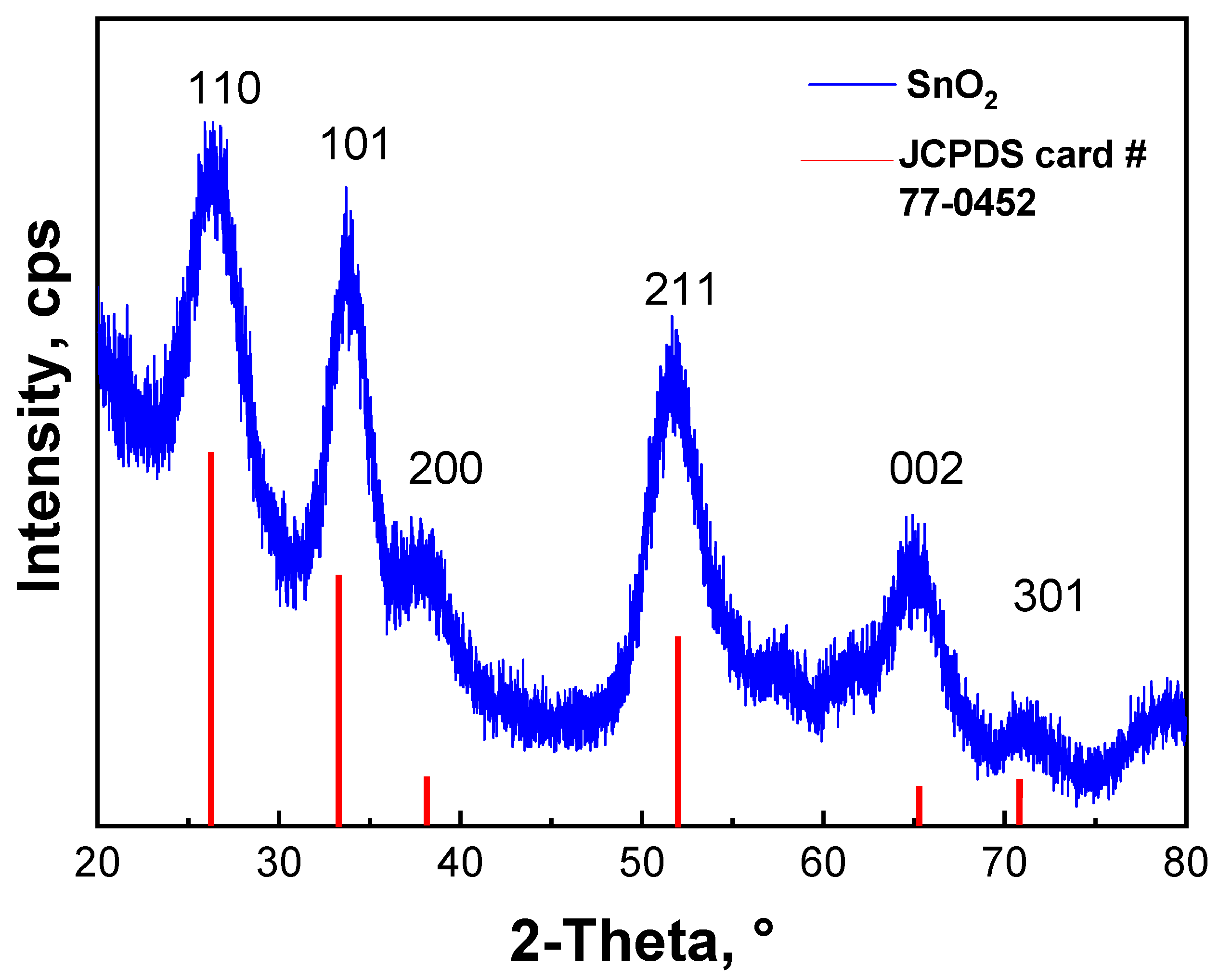
3.1. Crystallinity of SnO2 QDs

The XRD measurements were performed on as-prepared SnO2 QDs to analyze their structure. Figure 3 shows an XRD pattern of as-prepared SnO2 QDs. The XRD pattern shows the diffraction peaks at 2θ = 26.7°, 34.05°, 38.24°, 52.1°, 58.07°, 62.5°, and 65.00°, which correspond to the reflections from the (110), (101), (200), (211), (002), and (301) lattice planes of SnO2, respectively. All of the peaks match well with JCPDS Data Card No. 77-0452, indicating that the current structure is for SnO2, which exists in the tetragonal rutile crystalline phase. The crystal lattice parameters were calculated to be a = 0.4739 nm and c = 0.3221 nm (JCPDS card # 77-0452) [51,52,53]. The estimated average crystallite size for the SnO2 QDs is around 2.4 nm, which was calculated from the two major peaks at (110) and (211) using Scherrer’s equation (see Supporting Information) [38,39]. The full width at half-maximum (FWHM) values for the (110) and (211) peaks are about 3.6° and 3.5°, respectively.

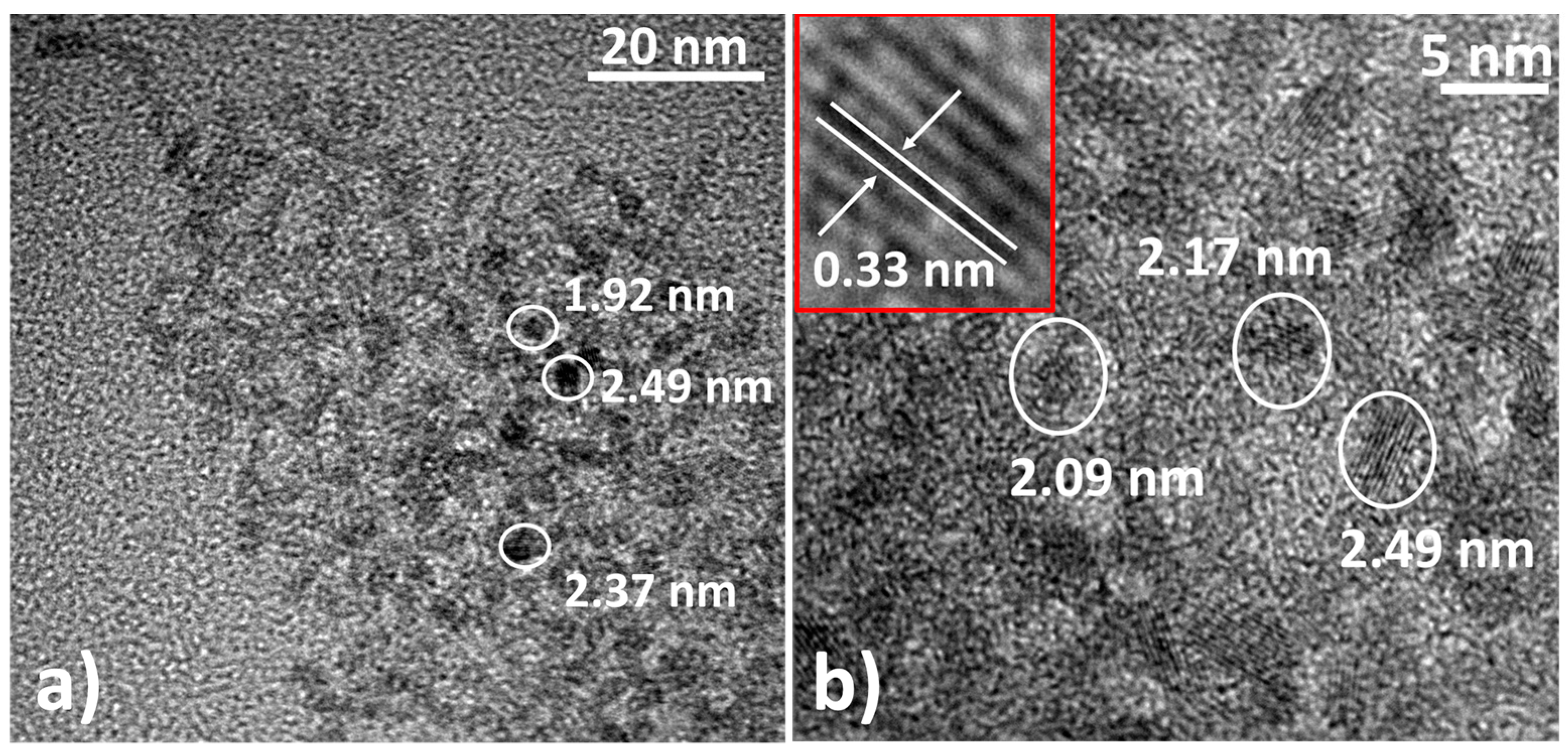
3.2. Transmission Electron Microscopy

A TEM analysis is conducted to obtain the electron micrographs of as-prepared SnO2 QDs and to estimate their particle size. The average particle size estimated from the TEM images (see Figure 4 and Figure S1 in Supporting Information) is around 2.4 nm, which is in good agreement with the crystallite size determined using the XRD data shown in Figure 3 [48]. The TEM image also indicates that the prepared particles have a uniform size distribution (Figure S1 in Supporting Information) and a crystalline structure, which is evident from the fringes shown in Figure 4b. The estimated value of d-spacing from the TEM image of the as-prepared SnO2 QDs is around 0.33 nm (see the inset image in Figure 4b). This corresponds to the {110} planes of SnO2. Since the size of the prepared SnO2 QDs is smaller than the Bohr exciton radius (around 2.7 nm), it is reasonable to state that the prepared particles are QDs of SnO2 [48,54].

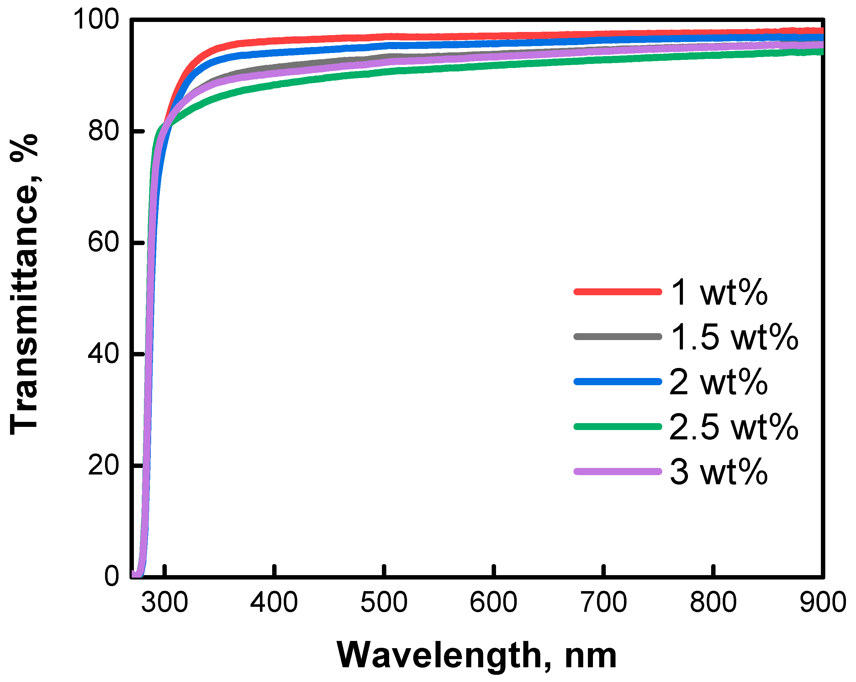
3.3. Optical Analysis

The investigation of the optical properties of the ETLs prepared using SnO2 inks with different SnO2 QD concentrations was carried out using a UV-Vis spectrometer. Figure 5 shows the measured transmittance spectra of the slot-die coated ETLs on glass substrates for the 250–900 nm wavelength range. A comparison of the UV-Vis spectra for different ETLs shows that the transmittance of the ETL made with a 1 wt% SnO2 QD ink is the highest and is well above 90% throughout the entire visible spectrum. The second highest transmittance is for the ETL made with a 2 wt% SnO2 QD ink, which is slightly higher than the one made with a 1.5 wt% SnO2 QD ink. The UV-Vis transmittance of the ETL made with a 3 wt% SnO2 QD ink is slightly lower than the one made with the 1.5 wt% SnO2 QD ink. The lowest transmittance is observed for the ETL made with a 2.5 wt% SnO2 QD ink. Overall, the UV-Vis transmittance measurements for the ETLs made with the 1, 2, and 3 wt% SnO2 QD inks show that, with an increase in the concentration of SnO2 QDs in the inks, the obtained ETL films become thicker. This is expected, since inks with a higher SnO2 QD content should produce thicker films. The observed minor inconsistencies with the ETLs made with the 1.5 and 2.5 wt% SnO2 QD inks could be associated with some small deviations in the ink preparation and deposition steps, which may influence the thickness of the resulting films. It is noteworthy to point out that the transmittance of all the ETLs is above 90%, which is beneficial from the PSC device perspective. Such high light transmittances of the obtained ETLs allow more photons to pass into the perovskite layer and enable the generation of more charge carriers in the complete devices [55,56,57,58].

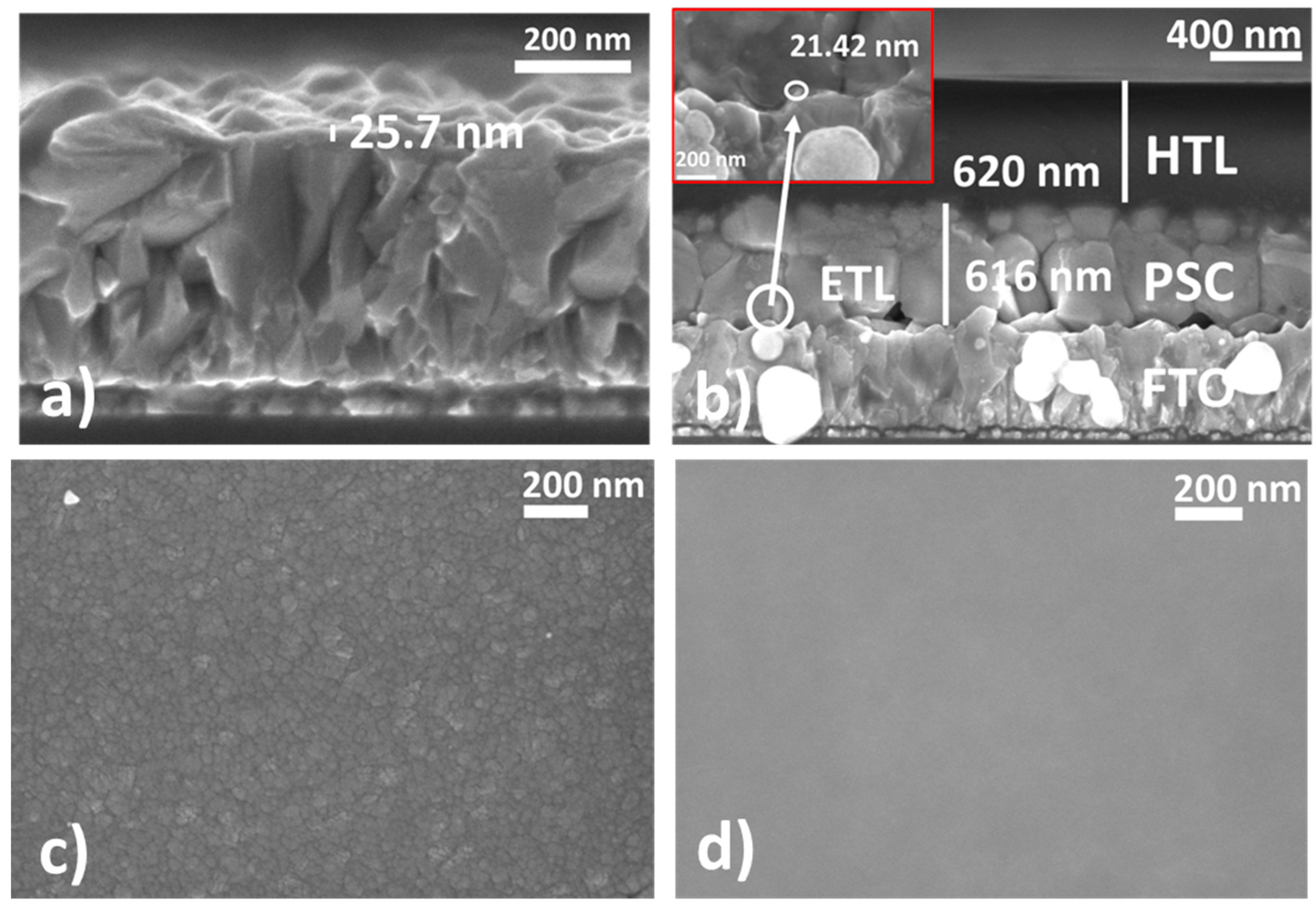
3.4. Scanning Electron Microscopy

The SEM imaging is used to determine the thickness of the device functional layers. Figure 6a shows the cross-section of an ETL on glass/FTO made using a 2 wt% SnO2 QD ink. The thickness of the SnO2 QD ETL is about 25 nm. The cross-section SEM images of ETLs made using the 1, 1.5, 2.5, and 3 wt% SnO2 QD inks are shown in Figure S2 in Supporting Information. Figure 6b shows all three functional layers of a PSC slot-die coated on glass/FTO. Here, the ETL is about 21–25 nm thick (see inset image), while the MAPbI3 and the HTL have thicknesses of around 600 and 650 nm, respectively. Figure 6c shows a top view SEM image of a bare PET/ITO substrate, in which the crystallites of the ITO layer are clearly visible. Figure 6d shows the top view SEM image of a 2 wt% SnO2 QD ETL slot-die coated on a PET/ITO substrate. The image indicates that the layer of SnO2 QDs completely covers the surface of the PET/ITO substrate, as no visible pinholes can be observed from the ETL through which the surface of the ITO can be seen. By comparing Figure 6c,d, the SnO2 QD ETL prepared by our technique can uniformly cover the surface of the PET/ITO substrate. A uniform coverage of the TCO layer by an ETL is necessary for good device operation.

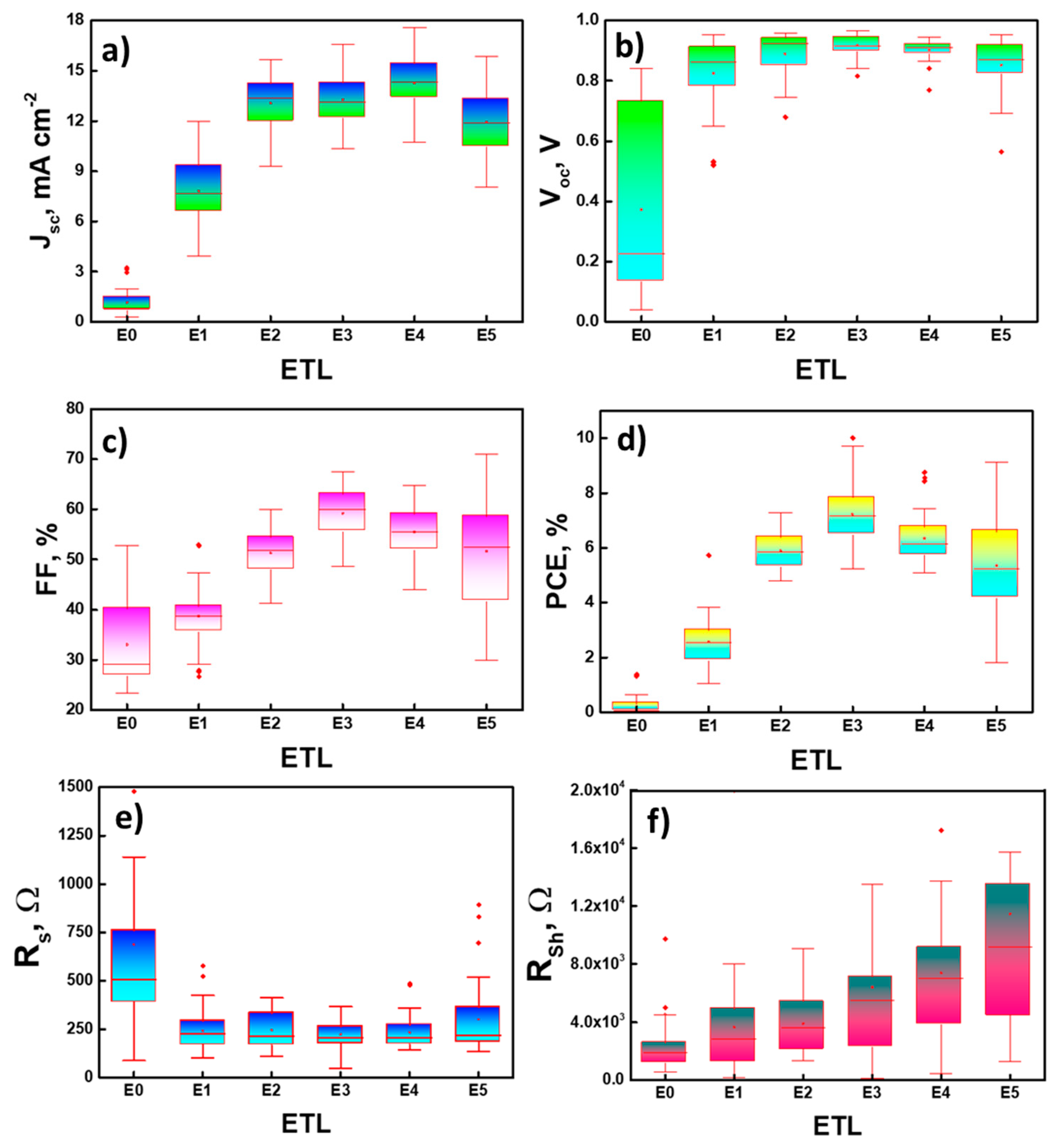
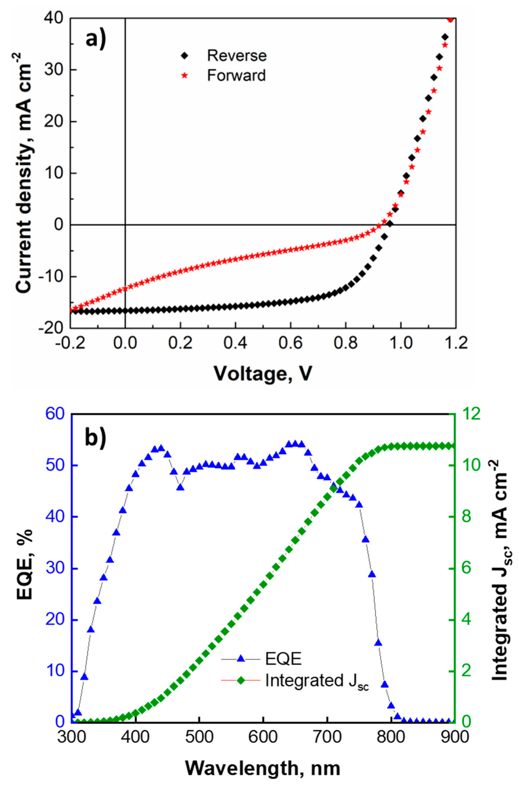
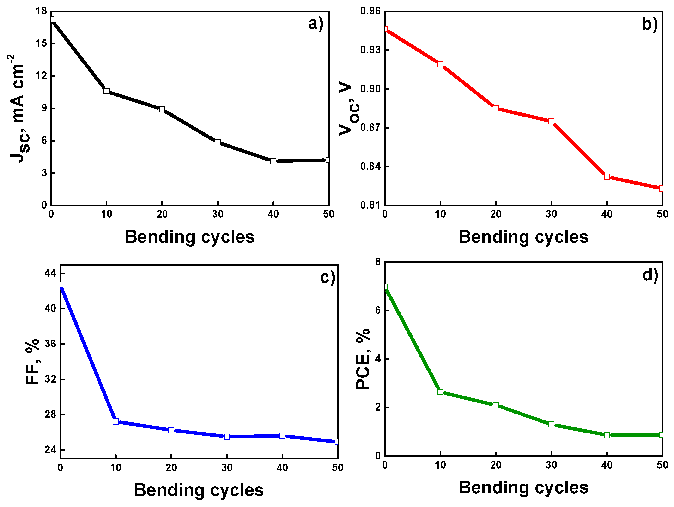
3.5. Device Analysis

Flexible and printed PSCs on PET/ITO substrates without and with ETLs, prepared using SnO2 QD solutions with different concentrations (0, 1, 1.5, 2, 2.5, and 3 wt%), were fabricated to rule out the suitable concentration of SnO2 QDs in the ETL inks. For this, devices are fabricated for each concentration of SnO2 QDs in the ETL inks. Hereon, the ETLs prepared with SnO2 QDs with 0, 1, 1.5, 2, 2.5, and 3 wt% will be referred to as E0, E1, E2, E3, E4, and E5, respectively. It should be noted that E0 refers to bare ITO. The prepared devices are tested, and a statistical analysis of the performance parameters of the top 40 well-performing devices for different ETLs (E0, E1, E2, E3, E4, and E5) is carried out.
Figure 7 shows the statistical data for the solar cell parameters (obtained from the reverse scans) such as open-circuit voltage (Voc), short-circuit current density (Jsc), fill factor (FF), PCE, series resistances (Rs), and shunt resistances (RSh) presented for devices with E0, E1, E2, E3, E4, and E5 ETLs. Figure 7a shows that the average Jsc values increase from E0 to E4. For E0, the Jsc value is around 1.12 mA cm−2, which, for E1, increases up to 7.7 mA cm−2. For E2, the Jsc value is 12.95 mA cm−2, which is higher than that in E1 by around 40%. The average Jsc value for E3 (13.28 mA cm−2) is only slightly higher than that in E2. The average Jsc value of E4 is about 14.31 mA cm−2, which is the highest among the compared devices. As for E5, there is a small drop in the average Jsc value as compared to E4. Figure 7b shows that there is also a continuous increase in the average Voc values from E0 to E3. The average Voc value in E3 is around 0.93 V, which is ~2.5 times higher than that in E0 and ~13% higher than that in E1. Afterwards, a continuous decrease in the average Voc values was observed for the devices with higher concentrations of SnO2 QDs in the ETL inks (E4 and E5).
The observed variations of the Voc and Jsc values with the change in the concentration of SnO2 QDs in the ETL inks might be due to the impact of the ETL morphology and thickness on the carrier recombination processes and series resistance in the devices (see Table 1) [59]. With an increase in the concentration of SnO2 QDs in the ETL ink, the resulting devices show higher RS values, as depicted in Figure 7e. The increase in RSh values with an increase in the concentration of SnO2 QDs in the ETL inks (see Figure 7f) might indicate that the resulting ETL becomes more compact and has fewer pinholes. This helps to reduce charge carrier back-reaction, which is possibly the reason for the initial increase in the average Voc and Jsc values (E0 to E3). The following decrease in the average Jsc value in E5 might originate from the suboptimal thickness of the ETL, which decreases the transmission of photons through the ETL (see Figure 5). As for the average Voc values in E4 and E5, it might be due to the higher charge recombination at the ETL/perovskite interface due to high the RS in the devices and the lower transmittance of the ETL films as compared to E3 [60].
Figure 7c depicts that there is a steep increase in the average FF values from E0 to E3, followed by a slow decrease for E4 and E5. This trend is somewhat similar to the ones observed in Voc and Jsc. The average FF value has a remarkable increase of around 37% when the SnO2 QD concentration in the ETL ink is doubled (from 1 wt% (E1) to 2 wt% (E3)). Generally, FF is a complex phenomenon. It depends on many device parameters and processes taking place in solar cells. Here, the initial increase in the average FF values from E0 to E3 could be associated with a decrease in the charge carrier recombination and, possibly, an increase in the electrical conductivity of the ETLs due to an increase in their thickness [61,62,63]. For E4 and E5, the decrease in FF might be due to an increase in RS in the devices [60].
The trends in the Voc, Jsc, and FF values determine the final trend for the overall variation of the average PCE with the change in the concentration of SnO2 QDs in the ETL inks. As expected and consistent with the variations in the average values of Voc, FF, and, to a certain extent, Jsc, the average PCE values of the devices increase from E0 to E3 and then decrease. The average PCE in E3 is almost three times higher than that in E1. This is mostly due to the significant increases in the average Jsc (by a factor of ~1.8) and FF (by a factor of ~1.5) values when the SnO2 QD concentration in the ETL ink is doubled (from 1 wt% (E1) to 2 wt% (E3)). All the devices with ETLs (E1, E2, E3, E4, and E5) have significantly higher performances compared to the devices without any ETL (E0). This indicates the necessity of ETLs to obtain a good performance of PSC devices. A detailed overview of the solar cell parameters is presented in Table 1. We note that most of the metal oxide (e.g., ZnO, SnO2, and NiO) inks that are commercially available and used in printed optoelectronic devices also have a metal oxide solid content at around 2–2.5 wt%. In light of this, the trends observed in this work appear reasonable and somewhat consistent with the commercially available inks [64,65,66,67].
The external quantum efficiency (EQE) measurements are also performed on the champion device with E3 ETL to obtain its spectral response. Figure 8b shows that the device has an EQE spectrum that is typical for the MAPbI3-based PSCs [68,69]. The device shows more or less stable EQE values at around 50% throughout the visible spectrum. The integrated Jsc value obtained from the EQE spectrum of the champion device is around 11 mA cm−2 (Figure 8b). This is comparable to the Jsc value of the device extracted from the J-V curve for the forward scan direction (see Table 2). The EQE spectra of the ’champion devices’ with E0, E1, E2, E4, and E5 ETLs are presented in Figure S4 in Supporting Information.
In order to study the mechanical stability of flexible PSCs, the fabricated device with E3 ETLs is subjected to a repeated cycle of compressive bending to a radius of around 1 cm, and their solar cell performance is measured after every 10 bending cycles. Overall, the devices are subjected to 50 bending cycles. Figure 9 shows the variations in the solar cell parameters of a device with E3 ETL upon bending. After the first 10 bending cycles, the Jsc value of the device decreases by 45%, and the FF value decreases by 37%. These fast decays in the Jsc and FF values after the first 10 bending cycles could mainly be associated with the deterioration of the structural integrity of the device due to the appearance of cracks in the ITO layer [70,71,72,73,74]. This significantly increases the device series resistance. Between the 10th and 50th bending cycles, the FF value of the device decays rather slowly and monotonously. A somewhat similar but slightly faster decay of the device’s Jsc value is observed for the same bending cycle range. These decays could be due to the further and more complex deterioration (e.g., micro-delamination of the device functional layers, formation of micro-cracks and micro-voids in the device[s functional layers, etc.) of the device’s structural integrity [75,76,77]. As for the device’s Voc, there is almost a linear decay trend with the increase in the number of bending cycles. This indicates the formation of many defects (microcracks) in the perovskite layer, which increases the rate of charge carrier recombination in the layer and leads to a corresponding decrease in the Voc and Jsc values of the devices [78,79,80,81]. These trends in the behavior of the Jsc, FF, and Voc during the bending test result in a fast decay of the device’s PCE after the first 10 bending cycles (a decrease from 7% to 2.5%) and a slower decay between the 10th and 50th bending cycles. After the 50th bending cycle, the PCE of the device becomes around 0.84%. This is smaller (by a factor of ~8) than the initial PCE value (7%) of the device. The mechanical stability could be further improved by the modification of the functional layers and their interfaces in PSCs as well as the application of more durable TCO layers [82].

4. Conclusions

In summary, the synthesis and application of SnO2 QDs as ETLs for flexible and printed PSCs based on PET/ITO substrates are demonstrated. SnO2 QDs with diameters around 2.4 nm are obtained using a solvothermal synthesis method. The QDs of SnO2 in the prepared inks are crystalline and well-dispersed. The device functional layers (ETL, perovskite, and HTL) are deposited using a slot-die coating method under ambient air conditions. In order to optimize the printed PSCs, the water-based inks with different SnO2 QD concentrations for preparing different thicknesses of ETLs are investigated. The devices with ETLs obtained by using a 2 wt% SnO2 QD ink show the best performance (the average PCE for the reverse scan direction is around 7.23%). The champion device, which shows a PCE value of around 10%, is also obtained with the ETL prepared using the 2 wt% SnO2 QD ink. The mechanical stability of a device with the 2 wt% SnO2 QD ETL is investigated by subjecting the device to a bending test. The initial fast degradation of the performance of the device is attributed to the cracking of the ITO layer in the device, whereas the further slower decay is a result of more complex deterioration in the structure of the device. The findings of the work can be useful in developing new electronic inks for optoelectronic applications and in establishing the advanced low-temperature manufacturing protocols for the printing of optoelectronic devices on heat-sensitive substrates.

Supplementary Materials

The following supporting information can be downloaded at: https://www.mdpi.com/article/10.3390/nano12152615/s1, Figure S1. Particle size distribution; Figure S2. SEM cross-section images of ETLs on glass/FTO made with (a) 1 wt%, (b) 1.5 wt%, (c) 2.5 wt% and, (d) 3 wt% of SnO2 QD inks; Figure S3. J-V curves of champion devices with (a) E0, (b) E1, (c) E2, (d) E4, and (e) E5 ETLs; Figure S4. EQE spectra of champion devices with different ETLs (E0, E1, E2, E4, and E5) [83,84].

Author Contributions

Conceptualization, A.N.J.; data curation, M.S.K.; formal analysis, A.N.J.; investigation, M.S.K., Z.T.S., A.G.K. and H.P.P.; methodology, M.S.K., Z.T.S., A.G.K., H.P.P. and A.N.J.; resources, A.N. and A.N.J.; supervision, A.N.J.; visualization, M.S.K., Z.T.S. and A.N.J.; writing—original draft, M.S.K.; writing—review and editing, A.N.J. All authors have read and agreed to the published version of the manuscript.

Funding

This research was funded by the Nazarbayev University Collaborative Research Grant (grant number: 021220CRP1922), the Young Scientist Grant of the Ministry of Education and Science of the Republic of Kazakhstan (grant number: AP08052412), and the Scientific Research Grant from the Ministry of Education and Science of the Republic of Kazakhstan (grant number: AP08856931).

Institutional Review Board Statement

Not applicable.

Informed Consent Statement

Not applicable.

Data Availability Statement

The data presented in this study are available on request from the corresponding author.

Acknowledgments

We would like to thank the Core Facilities team of Nazarbayev University for their help and support with the measurements (Erzhigit Sugurbekov for the XRD measurements; Nikita Alexandrovich Lutchenko for the TEM measurements; Laura Khamkash and Nurgul Daniyeva for the SEM measurements). A.N.J. appreciates the Nazarbayev University Collaborative Research Grant (grant number: 021220CRP1922) and the Young Scientist Grant of the Ministry of Education and Science of the Republic of Kazakhstan (grant number: AP08052412). A.N. appreciates the Scientific Research Grant from the Ministry of Education and Science of the Republic of Kazakhstan (grant number: AP08856931).

Conflicts of Interest

The authors declare no conflict of interest.

References

  1. Ashina, A.; Battula, R.K.; Ramasamy, E.; Chundi, N.; Sakthivel, S.; Veerappan, G. Dip Coated SnO2 Film as Electron Transport Layer for Low Temperature Processed Planar Perovskite Solar Cells. Appl. Surf. Sci. Adv. 2021, 4, 100066. [Google Scholar] [CrossRef]
  2. Cao, J.-J.; Wang, K.-L.; Dong, C.; Li, X.-M.; Yang, W.-F.; Wang, Z.-K. Bottom-Contact Passivation for High-Performance Perovskite Solar Cells Using TaCl5-Doped SnO2 as Electron-Transporting Layer. Org. Electron. 2021, 88, 105972. [Google Scholar] [CrossRef]
  3. Jung, E.H.; Jeon, N.J.; Park, E.Y.; Moon, C.S.; Shin, T.J.; Yang, T.-Y.; Noh, J.H.; Seo, J. Efficient, Stable and Scalable Perovskite Solar Cells Using Poly(3-Hexylthiophene). Nature 2019, 567, 511–515. [Google Scholar] [CrossRef] [PubMed]
  4. Razza, S.; Castro-Hermosa, S.; Di Carlo, A.; Brown, T.M. Research Update: Large-Area Deposition, Coating, Printing, and Processing Techniques for the Upscaling of Perovskite Solar Cell Technology. APL Mater. 2016, 4, 091508. [Google Scholar] [CrossRef] [Green Version]
  5. Cai, B.; Zhang, W.-H.; Qiu, J. Solvent Engineering of Spin-Coating Solutions for Planar-Structured High-Efficiency Perovskite Solar Cells. Chin. J. Catal. 2015, 36, 1183–1190. [Google Scholar] [CrossRef]
  6. Zhang, Z.; Wei, D.; Xie, B.; Yue, X.; Li, M.; Song, D.; Li, Y. High Reproducibility of Perovskite Solar Cells via a Complete Spin-Coating Sequential Solution Deposition Process. Sol. Energy 2015, 122, 97–103. [Google Scholar] [CrossRef]
  7. Gong, C.; Tong, S.; Huang, K.; Li, H.; Huang, H.; Zhang, J.; Yang, J. Flexible Planar Heterojunction Perovskite Solar Cells Fabricated via Sequential Roll-to-Roll Microgravure Printing and Slot-Die Coating Deposition. Sol. RRL 2020, 4, 1900204. [Google Scholar] [CrossRef]
  8. Zheng, J.; Zhang, M.; Lau, C.F.J.; Deng, X.; Kim, J.; Ma, Q.; Chen, C.; Green, M.A.; Huang, S.; Ho-Baillie, A.W.Y. Spin-Coating Free Fabrication for Highly Efficient Perovskite Solar Cells. Sol. Energy Mater. Sol. Cells 2017, 168, 165–171. [Google Scholar] [CrossRef]
  9. Whitaker, J.B.; Hoe Kim, D.; Larson, B.W.; Zhang, F.; Berry, J.J.; van Hest, M.F.A.M.; Zhu, K. Scalable Slot-Die Coating of High Performance Perovskite Solar Cells. Sustain. Energy Fuels 2018, 2, 2442–2449. [Google Scholar] [CrossRef]
  10. Sandström, A.; Dam, H.F.; Krebs, F.C.; Edman, L. Ambient Fabrication of Flexible and Large-Area Organic Light-Emitting Devices Using Slot-Die Coating. Nat. Commun. 2012, 3, 1002. [Google Scholar] [CrossRef] [Green Version]
  11. Zhu, S.; Tian, J.; Zhang, J.; Gao, C.; Liu, X. Improving the Interfacial Contact of Screen-Printed Carbon Electrodes for Perovskite Solar Cells. ACS Appl. Energy Mater. 2021, 4, 5554–5559. [Google Scholar] [CrossRef]
  12. Cao, K.; Zuo, Z.; Cui, J.; Shen, Y.; Moehl, T.; Zakeeruddin, S.M.; Grätzel, M.; Wang, M. Efficient Screen Printed Perovskite Solar Cells Based on Mesoscopic TiO2/Al2O3/NiO/Carbon Architecture. Nano Energy 2015, 17, 171–179. [Google Scholar] [CrossRef]
  13. Yang, J.; Lim, E.L.; Tan, L.; Wei, Z. Ink Engineering in Blade-Coating Large-Area Perovskite Solar Cells. Adv. Energy Mater. 2022, 12, 2200975. [Google Scholar] [CrossRef]
  14. Gao, B.; Meng, J. Flexible CH3NH3PbI3 Perovskite Solar Cells with High Stability Based on All Inkjet Printing. Sol. Energy 2021, 230, 598–604. [Google Scholar] [CrossRef]
  15. Gao, L.; Huang, K.; Long, C.; Zeng, F.; Liu, B.; Yang, J. Fully Slot-Die-Coated Perovskite Solar Cells in Ambient Condition. Appl. Phys. A 2020, 126, 452. [Google Scholar] [CrossRef]
  16. Mathiazhagan, G.; Seeber, A.; Gengenbach, T.; Mastroianni, S.; Vak, D.; Chesman, A.S.R.; Gao, M.; Angmo, D.; Hinsch, A. Improving the Stability of Ambient Processed, SnO2-Based, Perovskite Solar Cells by the UV-Treatment of Sub-Cells. Sol. RRL 2020, 4, 2000262. [Google Scholar] [CrossRef]
  17. Bahadur, J.; Ghahremani, A.H.; Martin, B.; Druffel, T.; Sunkara, M.K.; Pal, K. Solution Processed Mo Doped SnO2 as an Effective ETL in the Fabrication of Low Temperature Planer Perovskite Solar Cell under Ambient Conditions. Org. Electron. 2019, 67, 159–167. [Google Scholar] [CrossRef]
  18. Tzounis, L.; Stergiopoulos, T.; Zachariadis, A.; Gravalidis, C.; Laskarakis, A.; Logothetidis, S. Perovskite Solar Cells from Small Scale Spin Coating Process towards Roll-to-Roll Printing: Optical and Morphological Studies. Mater. Today Proc. 2017, 4, 5082–5089. [Google Scholar] [CrossRef]
  19. Brunetti, F.; Operamolla, A.; Castro-Hermosa, S.; Lucarelli, G.; Manca, V.; Farinola, G.M.; Brown, T.M. Printed Solar Cells and Energy Storage Devices on Paper Substrates. Adv. Funct. Mater. 2019, 29, 1806798. [Google Scholar] [CrossRef] [Green Version]
  20. Maafa, I.M. All-Inorganic Perovskite Solar Cells: Recent Advancements and Challenges. Nanomaterials 2022, 12, 1651. [Google Scholar] [CrossRef] [PubMed]
  21. Afre, R.A.; Sharma, N.; Sharon, M.; Sharon, M. Transparent Conducting Oxide Films for Various Applications: A Review. Rev. Adv. Mater. Sci. 2018, 53, 79–89. [Google Scholar] [CrossRef]
  22. Choi, Y.J.; Lee, H.Y.; Kim, S.; Song, P.K. Controlled Lattice Thermal Conductivity of Transparent Conductive Oxide Thin Film via Localized Vibration of Doping Atoms. Nanomaterials 2021, 11, 2363. [Google Scholar] [CrossRef] [PubMed]
  23. Mohanraj, J.; Singh, C.R.; Gujar, T.P.; Heinrich, C.D.; Thelakkat, M. Nanostructured Hybrid Metal Mesh as Transparent Conducting Electrodes: Selection Criteria Verification in Perovskite Solar Cells. Nanomaterials 2021, 11, 1783. [Google Scholar] [CrossRef] [PubMed]
  24. Zhu, N.; Qi, X.; Zhang, Y.; Liu, G.; Wu, C.; Wang, D.; Guo, X.; Luo, W.; Li, X.; Hu, H.; et al. High Efficiency (18.53%) of Flexible Perovskite Solar Cells via the Insertion of Potassium Chloride between SnO2 and CH3NH 3PbI 3 Layers. ACS Appl. Energy Mater. 2019, 2, 3676–3682. [Google Scholar] [CrossRef]
  25. Rieu, M.; Camara, M.; Tournier, G.; Viricelle, J.-P.; Pijolat, C.; de Rooij, N.F.; Briand, D. Fully Inkjet Printed SnO2 Gas Sensor on Plastic Substrate. Sens. Actuators B Chem. 2016, 236, 1091–1097. [Google Scholar] [CrossRef] [Green Version]
  26. Dong, J.; Jia, J.; Feng, X.; Shi, B.; Wu, Y.; Zhang, Y.; Wu, J.; Cao, B. Ligand Exchange of SnO2 Effectively Improving the Efficiency of Flexible Perovskite Solar Cells. J. Alloys Compd. 2021, 883, 160827. [Google Scholar] [CrossRef]
  27. Wang, H.; Cao, S.; Yang, B.; Li, H.; Wang, M.; Hu, X.; Sun, K.; Zang, Z. NH4Cl-Modified ZnO for High-Performance CsPbIBr2 Perovskite Solar Cells via Low-Temperature Process. Sol. RRL 2020, 4, 1900363. [Google Scholar] [CrossRef]
  28. Liu, J.; He, X.; Li, X.; Li, Y. Solvent-Assisted Preparation of Low-Temperature SnO2 Electron Transport Layers for Efficient and Stable Perovskite Solar Cells Made in Ambient Conditions. New J. Chem. 2022, 46, 9841–9850. [Google Scholar] [CrossRef]
  29. Cao, Z.; Li, C.; Deng, X.; Wang, S.; Yuan, Y.; Chen, Y.; Wang, Z.; Liu, Y.; Ding, L.; Hao, F. Metal Oxide Alternatives for Efficient Electron Transport in Perovskite Solar Cells: Beyond TiO2 and SnO2. J. Mater. Chem. A 2020, 8, 19768–19787. [Google Scholar] [CrossRef]
  30. Lin, H.-K.; Li, J.-X.; Wang, H.-C.; Su, Y.-W.; Wu, K.-H.; Wei, K.-H. Dual Nanocomposite Carrier Transport Layers Enhance the Efficiency of Planar Perovskite Photovoltaics. RSC Adv. 2018, 8, 12526–12534. [Google Scholar] [CrossRef] [Green Version]
  31. Wang, P.; Shao, Z.; Ulfa, M.; Pauporté, T. Insights into the Hole Blocking Layer Effect on the Perovskite Solar Cell Performance and Impedance Response. J. Phys. Chem. C 2017, 121, 9131–9141. [Google Scholar] [CrossRef]
  32. Chen, Y.; Meng, Q.; Zhang, L.; Han, C.; Gao, H.; Zhang, Y.; Yan, H. SnO2-Based Electron Transporting Layer Materials for Perovskite Solar Cells: A Review of Recent Progress. J. Energy Chem. 2019, 35, 144–167. [Google Scholar] [CrossRef] [Green Version]
  33. Shi, S.; Li, J.; Bu, T.; Yang, S.; Xiao, J.; Peng, Y.; Li, W.; Zhong, J.; Ku, Z.; Cheng, Y.-B.; et al. Room-Temperature Synthesized SnO2 Electron Transport Layers for Efficient Perovskite Solar Cells. RSC Adv. 2019, 9, 9946–9950. [Google Scholar] [CrossRef] [PubMed] [Green Version]
  34. Ai, Y.; Zhang, Y.; Song, J.; Kong, T.; Li, Y.; Xie, H.; Bi, D. In Situ Perovskitoid Engineering at SnO2 Interface toward Highly Efficient and Stable Formamidinium Lead Triiodide Perovskite Solar Cells. J. Phys. Chem. Lett. 2021, 12, 10567–10573. [Google Scholar] [CrossRef] [PubMed]
  35. Lu, D.; Zhang, W.; Kloo, L.; Belova, L. Inkjet-Printed Electron Transport Layers for Perovskite Solar Cells. Materials 2021, 14, 7525. [Google Scholar] [CrossRef]
  36. Jiang, Y.; Sun, L.; Jiang, F.; Xie, C.; Hu, L.; Dong, X.; Qin, F.; Liu, T.; Hu, L.; Jiang, X.; et al. Photocatalytic Effect of ZnO on the Stability of Nonfullerene Acceptors and Its Mitigation by SnO2 for Nonfullerene Organic Solar Cells. Mater. Horiz. 2019, 6, 1438–1443. [Google Scholar] [CrossRef]
  37. Dkhissi, Y.; Huang, F.; Rubanov, S.; Xiao, M.; Bach, U.; Spiccia, L.; Caruso, R.A.; Cheng, Y.-B. Low Temperature Processing of Flexible Planar Perovskite Solar Cells with Efficiency over 10%. J. Power Sources 2015, 278, 325–331. [Google Scholar] [CrossRef]
  38. Halvani Anaraki, E.; Kermanpur, A.; Steier, L.; Domanski, K.; Matsui, T.; Tress, W.; Saliba, M.; Abate, A.; Grätzel, M.; Hagfeldt, A.; et al. Highly Efficient and Stable Planar Perovskite Solar Cells by Solution-Processed Tin Oxide. Energy Environ. Sci. 2016, 9, 3128–3134. [Google Scholar] [CrossRef]
  39. Ke, W.; Fang, G.; Liu, Q.; Xiong, L.; Qin, P.; Tao, H.; Wang, J.; Lei, H.; Li, B.; Wan, J.; et al. Low-Temperature Solution-Processed Tin Oxide as an Alternative Electron Transporting Layer for Efficient Perovskite Solar Cells. J. Am. Chem. Soc. 2015, 137, 6730–6733. [Google Scholar] [CrossRef]
  40. Bu, T.; Li, J.; Zheng, F.; Chen, W.; Wen, X.; Ku, Z.; Peng, Y.; Zhong, J.; Cheng, Y.-B.; Huang, F. Universal Passivation Strategy to Slot-Die Printed SnO2 for Hysteresis-Free Efficient Flexible Perovskite Solar Module. Nat. Commun. 2018, 9, 4609. [Google Scholar] [CrossRef] [Green Version]
  41. Vijayaraghavan, S.N.; Wall, J.; Li, L.; Xing, G.; Zhang, Q.; Yan, F. Low-Temperature Processed Highly Efficient Hole Transport Layer Free Carbon-Based Planar Perovskite Solar Cells with SnO2 Quantum Dot Electron Transport Layer. Mater. Today Phys. 2020, 13, 100204. [Google Scholar] [CrossRef]
  42. Ren, Z.; Liu, K.; Hu, H.; Guo, X.; Gao, Y.; Fong, P.W.K.; Liang, Q.; Tang, H.; Huang, J.; Zhang, H.; et al. Room-Temperature Multiple Ligands-Tailored SnO2 Quantum Dots Endow in Situ Dual-Interface Binding for Upscaling Efficient Perovskite Photovoltaics with High VOC. Light Sci. Appl. 2021, 10, 239. [Google Scholar] [CrossRef] [PubMed]
  43. Sheikh, S.P.; Reddy, V.R.; Sen, P. Size-Dependent Nonlinear Optical Absorption in SnO2 Quantum Dots. J. Opt. Soc. Am. B 2020, 37, 2788–2795. [Google Scholar] [CrossRef]
  44. Tong, G.; Ono, L.K.; Liu, Y.; Zhang, H.; Bu, T.; Qi, Y. Up-Scalable Fabrication of SnO2 with Multifunctional Interface for High Performance Perovskite Solar Modules. Nano-Micro Lett. 2021, 13, 155. [Google Scholar] [CrossRef] [PubMed]
  45. Zhang, J.; Zhang, W.; Cheng, H.-M.; Silva, S.R.P. Critical Review of Recent Progress of Flexible Perovskite Solar Cells. Mater. Today 2020, 39, 66–88. [Google Scholar] [CrossRef]
  46. Ahsan Saeed, M.; Hyeon Kim, S.; Baek, K.; Hyun, J.K.; Youn Lee, S.; Won Shim, J. PEDOT:PSS: CuNW-Based Transparent Composite Electrodes for High-Performance and Flexible Organic Photovoltaics under Indoor Lighting. Appl. Surf. Sci. 2021, 567, 150852. [Google Scholar] [CrossRef]
  47. Liu, J.; Xue, W.; Jin, G.; Zhai, Z.; Lv, J.; Hong, W.; Chen, Y. Preparation of Tin Oxide Quantum Dots in Aqueous Solution and Applications in Semiconductor Gas Sensors. Nanomaterials 2019, 9, 240. [Google Scholar] [CrossRef] [Green Version]
  48. Zhu, H.; Yang, D.; Yu, G.; Zhang, H.; Yao, K. A Simple Hydrothermal Route for Synthesizing SnO2quantum Dots. Nanotechnology 2006, 17, 2386–2389. [Google Scholar] [CrossRef] [Green Version]
  49. Hussain, I.; Tran, H.P.; Jaksik, J.; Moore, J.; Islam, N.; Uddin, M.J. Functional Materials, Device Architecture, and Flexibility of Perovskite Solar Cell. Emergent Mater. 2018, 1, 133–154. [Google Scholar] [CrossRef] [Green Version]
  50. Lu, C.; Zhang, W.; Jiang, Z.; Zhang, Y.; Ni, C. CuI/Spiro-OMeTAD Double-Layer Hole Transport Layer to Improve Photovoltaic Performance of Perovskite Solar Cells. Coatings 2021, 11, 978. [Google Scholar] [CrossRef]
  51. Chen, W.; Zhou, Q.; Wan, F.; Gao, T. Gas Sensing Properties and Mechanism of Nano-SnO2-Based Sensor for Hydrogen and Carbon Monoxide. J. Nanomater. 2012, 2012, 612420. [Google Scholar] [CrossRef] [Green Version]
  52. Lamdhade, G.T.; Raghuwanshi, F.C.; Agrawal, R.M.; Balkhande, V.M.; Shripath, T. SnO2 Nanoparticles Synthesis Via Liquid-Phase Co-Precipitation Technique. Adv. Mater. Lett. 2015, 6, 738–742. [Google Scholar] [CrossRef]
  53. Rani, R.; Sharma, S. Preparation and Characterization of SnO2 Nanofibers via Electrospinning. Adv. Nanoparticles 2016, 5, 53–59. [Google Scholar] [CrossRef] [Green Version]
  54. Bhattacharjee, A.; Ahmaruzzaman, M. A Novel and Green Process for the Production of Tin Oxide Quantum Dots and Its Application as a Photocatalyst for the Degradation of Dyes from Aqueous Phase. J. Colloid Interface Sci. 2015, 448, 130–139. [Google Scholar] [CrossRef]
  55. Xie, J.; Huang, K.; Yu, X.; Yang, Z.; Xiao, K.; Qiang, Y.; Zhu, X.; Xu, L.; Wang, P.; Cui, C.; et al. Enhanced Electronic Properties of SnO2 via Electron Transfer from Graphene Quantum Dots for Efficient Perovskite Solar Cells. ACS Nano 2017, 11, 9176–9182. [Google Scholar] [CrossRef]
  56. Ou, X.-L.; Feng, J.; Xu, M.; Sun, H.-B. Semitransparent and Flexible Perovskite Solar Cell with High Visible Transmittance Based on Ultrathin Metallic Electrodes. Opt. Lett. 2017, 42, 1958–1961. [Google Scholar] [CrossRef]
  57. Remarkably High Performance of Organic Photovoltaic Devices with 3,9-Bis(2-Methylene-(3-(1,1-Dicyanomethylene)-Indanone))-5,5,11,11-Tetrakis(4-Hexyl Meta-Phenyl)-Dithieno[2,3-d:2′,3′-d′]-s-Indaceno[1,2-b:5,6-b′]Dithiophene)- Ethylhexyloxy] Photoactive Acceptor under Halogen Light Illumination-ScienceDirect. Available online: https://www.sciencedirect.com/science/article/pii/S0378775321012738 (accessed on 30 June 2022).
  58. Elastomeric Indoor Organic Photovoltaics with Superb Photothermal Endurance-Kim-Advanced Functional Materials-Wiley Online Library. Available online: https://onlinelibrary.wiley.com/doi/abs/10.1002/adfm.202201921 (accessed on 30 June 2022).
  59. Jeyakumar, R.; Bag, A.; Nekovei, R.; Radhakrishnan, R. Influence of Electron Transport Layer (TiO2) Thickness and Its Doping Density on the Performance of CH3NH3PbI3-Based Planar Perovskite Solar Cells. J. Electron. Mater. 2020, 49, 3533–3539. [Google Scholar] [CrossRef] [Green Version]
  60. Impact of Interfacial Layers in Perovskite Solar Cells-Cho-2017-ChemSusChem-Wiley Online Library. Available online: https://chemistry-europe.onlinelibrary.wiley.com/doi/full/10.1002/cssc.201701095 (accessed on 31 May 2022).
  61. Habisreutinger, S.N.; Noel, N.K.; Snaith, H.J. Hysteresis Index: A Figure without Merit for Quantifying Hysteresis in Perovskite Solar Cells. ACS Energy Lett. 2018, 3, 2472–2476. [Google Scholar] [CrossRef] [Green Version]
  62. Cao, Q.; Li, Y.; Zhang, H.; Yang, J.; Han, J.; Xu, T.; Wang, S.; Wang, Z.; Gao, B.; Zhao, J.; et al. Efficient and Stable Inverted Perovskite Solar Cells with Very High Fill Factors via Incorporation of Star-Shaped Polymer. Sci. Adv. 2021, 7, eabg0633. [Google Scholar] [CrossRef]
  63. Rai, M.; Wong, L.H.; Etgar, L. Effect of Perovskite Thickness on Electroluminescence and Solar Cell Conversion Efficiency. J. Phys. Chem. Lett. 2020, 11, 8189–8194. [Google Scholar] [CrossRef]
  64. Tan, H.; Jain, A.; Voznyy, O.; Lan, X.; García de Arquer, F.P.; Fan, J.Z.; Quintero-Bermudez, R.; Yuan, M.; Zhang, B.; Zhao, Y.; et al. Efficient and Stable Solution-Processed Planar Perovskite Solar Cells via Contact Passivation. Science 2017, 355, 722–726. [Google Scholar] [CrossRef] [PubMed]
  65. Weber, S.; Rath, T.; Mangalam, J.; Kunert, B.; Coclite, A.M.; Bauch, M.; Dimopoulos, T.; Trimmel, G. Investigation of NiOx-Hole Transport Layers in Triple Cation Perovskite Solar Cells. J. Mater. Sci. Mater. Electron. 2018, 29, 1847–1855. [Google Scholar] [CrossRef] [Green Version]
  66. Bush, K.A.; Bailie, C.D.; Chen, Y.; Bowring, A.R.; Wang, W.; Ma, W.; Leijtens, T.; Moghadam, F.; McGehee, M.D. Thermal and Environmental Stability of Semi-Transparent Perovskite Solar Cells for Tandems Enabled by a Solution-Processed Nanoparticle Buffer Layer and Sputtered ITO Electrode. Adv. Mater. 2016, 28, 3937–3943. [Google Scholar] [CrossRef]
  67. Hoang, V.Q.; Lee, S.K.; Bark, C.W. Dispersed SnO2 Colloids Using Sodium Dodecyl Benzene Sulfonate for High-Performance Planar Perovskite Solar Cells. Sol. Energy 2021, 230, 747–753. [Google Scholar] [CrossRef]
  68. Chander, S.; Purohit, A.; Nehra, A.; Nehra, S.P.; Dhaka, M.S. A Study on Spectral Response and External Quantum Efficiency of Mono-Crystalline Silicon Solar Cell. Int. J. Renew. Energy Res. 2015, 4, 41–44. [Google Scholar]
  69. Slami, A.; Benramdane, N. Manual Method for Measuring The External Quantum Efficiency for Solar Cells. E3S Web Conf. 2021, 229, 01005. [Google Scholar] [CrossRef]
  70. Jo Kim, B.; Hoe Kim, D.; Lee, Y.-Y.; Shin, H.-W.; Sang Han, G.; Sug Hong, J.; Mahmood, K.; Kyu Ahn, T.; Joo, Y.-C.; Sun Hong, K.; et al. Highly Efficient and Bending Durable Perovskite Solar Cells: Toward a Wearable Power Source. Energy Environ. Sci. 2015, 8, 916–921. [Google Scholar] [CrossRef]
  71. Wang, C.; Guan, L.; Zhao, D.; Yu, Y.; Grice, C.R.; Song, Z.; Awni, R.A.; Chen, J.; Wang, J.; Zhao, X.; et al. Water Vapor Treatment of Low-Temperature Deposited SnO2 Electron Selective Layers for Efficient Flexible Perovskite Solar Cells. ACS Energy Lett. 2017, 2, 2118–2124. [Google Scholar] [CrossRef]
  72. Yang, F.; Liu, J.; Lim, H.E.; Ishikura, Y.; Shinokita, K.; Miyauchi, Y.; Wakamiya, A.; Murata, Y.; Matsuda, K. High Bending Durability of Efficient Flexible Perovskite Solar Cells Using Metal Oxide Electron Transport Layer. J. Phys. Chem. C 2018, 122, 17088–17095. Available online: https://pubs.acs.org/doi/10.1021/acs.jpcc.8b05008 (accessed on 12 July 2022). [CrossRef]
  73. Heo, J.H.; Shin, D.H.; Jang, M.H.; Lee, M.L.; Kang, M.G.; Im, S.H. Highly Flexible, High-Performance Perovskite Solar Cells with Adhesion Promoted AuCl3-Doped Graphene Electrodes. J. Mater. Chem. A 2017, 5, 21146–21152. [Google Scholar] [CrossRef]
  74. Popoola, I.K.; Gondal, M.A.; Qahtan, T.F. Recent Progress in Flexible Perovskite Solar Cells: Materials, Mechanical Tolerance and Stability. Renew. Sustain. Energy Rev. 2018, 82, 3127–3151. [Google Scholar] [CrossRef]
  75. Xu, Y.; Lin, Z.; Wei, W.; Hao, Y.; Liu, S.; Ouyang, J.; Chang, J. Recent Progress of Electrode Materials for Flexible Perovskite Solar Cells. Nano-Micro Lett. 2022, 14, 117. [Google Scholar] [CrossRef] [PubMed]
  76. Flexible Perovskite Solar Cells with Simultaneously Improved Efficiency, Operational Stability, and Mechanical Reliability-ScienceDirect. Available online: https://www.sciencedirect.com/science/article/pii/S2542435121002002?via%3Dihub (accessed on 12 July 2022).
  77. Record Efficiency Stable Flexible Perovskite Solar Cell Using Effective Additive Assistant Strategy-Feng-2018-Advanced Materials-Wiley Online Library. Available online: https://onlinelibrary.wiley.com/doi/full/10.1002/adma.201801418 (accessed on 12 July 2022).
  78. Lee, G.; Kim, M.; Choi, Y.W.; Ahn, N.; Jang, J.; Yoon, J.; Kim, S.M.; Lee, J.-G.; Kang, D.; Jung, H.S.; et al. Ultra-Flexible Perovskite Solar Cells with Crumpling Durability: Toward a Wearable Power Source. Energy Environ. Sci. 2019, 12, 3182–3191. [Google Scholar] [CrossRef]
  79. Cheacharoen, R.; Rolston, N.; Harwood, D.; Bush, K.A.; Dauskardt, R.H.; McGehee, M.D. Design and Understanding of Encapsulated Perovskite Solar Cells to Withstand Temperature Cycling. Energy Environ. Sci. 2018, 11, 144–150. [Google Scholar] [CrossRef]
  80. Jiang, N.R.; Wang, Y.F.; Dong, Q.F.; Ge, C.D.; Yang, Z.Q.; Yin, D. Enhanced Efficiency and Mechanical Robustness of Flexible Perovskite Solar Cells by Using HPbI3 Additive. Sol. RRL 2021, 5, 2000821. Available online: https://onlinelibrary.wiley.com/doi/abs/10.1002/solr.202000821 (accessed on 12 July 2022). [CrossRef]
  81. Impact of Interlayer Application on Band Bending for Improved Electron Extraction for Efficient Flexible Perovskite Mini-Modules-ScienceDirect. Available online: https://www.sciencedirect.com/science/article/pii/S2211285518302866?via%3Dihub (accessed on 12 July 2022).
  82. Sears, K.K.; Fievez, M.; Gao, M.; Weerasinghe, H.C.; Easton, C.D.; Vak, D. ITO-Free Flexible Perovskite Solar Cells Based on Roll-to-Roll, Slot-Die Coated Silver Nanowire Electrodes. Sol. RRL 2017, 9, 1700059. [Google Scholar] [CrossRef]
  83. Patterson, A.L. The Scherrer Formula for X-Ray Particle Size Determination. Phys. Rev. 1939, 56, 978–982. [Google Scholar] [CrossRef]
  84. Bokuniaeva, A.O.; Vorokh, A.S. Estimation of Particle Size Using the Debye Equation and the Scherrer Formula for Polyphasic TiO2 Powder. J. Phys. 2019, 1410, 012057. [Google Scholar] [CrossRef]
Figure 1. Preparation of ETL ink with SnO2 QDs.
Nanomaterials 12 02615 g001
Figure 2. (a) Schematic diagram of the device fabrication process. (b) Energy level diagram for PSCs.
Nanomaterials 12 02615 g002
Figure 3. XRD pattern of as-prepared SnO2 QDs.
Nanomaterials 12 02615 g003
Figure 4. TEM micrographs of SnO2 QDs synthesized via a solvothermal route at a magnification of (a) 40 kX and (b) 1500 kX. The inset image in (b) shows the fringes and d-spacing of SnO2 QDs.
Nanomaterials 12 02615 g004
Figure 5. UV-Vis transmittance spectra of ETLs on glass substrates prepared using ETL inks with different SnO2 QD concentrations.
Nanomaterials 12 02615 g005
Figure 6. (a) SEM cross-section view of the ETL with SnO2 QDs on glass/FTO. (b) SEM cross-section view of slot-die coated device functional layers on glass/FTO (inset shows the presence of ETL between the FTO and perovskite layers. (c) SEM top view image of the PET/ITO substrate (magnification at 100 kX). (d) SEM top view image of the SnO2 QD ETL on the PET/ITO substrate (magnification at 100 kX).
Nanomaterials 12 02615 g006
Figure 7. Comparison of the average values of (a) Jsc, (b) Voc, (c) FF, (d) PCE, (e) RS, and (f) RSh of printed and flexible PSCs for different SnO2 ETLs prepared using SnO2 QD inks with different QD concentrations.
Nanomaterials 12 02615 g007
Figure 8. (a) J-V curves and (b) EQE spectrum with an integrated Jsc curve for the champion device.
Nanomaterials 12 02615 g008
Figure 9. Variation in the (a) Jsc, (b) Voc, (c) FF, and (d) PCE of the device upon bending.
Nanomaterials 12 02615 g009
Table 1. Statistical analysis of the performance parameters of the top 40 well-performing devices for different ETLs.
ETLs.Scan DirectionJsc, mA cm−2Voc, VFF, %PCE, %RS, ΩRSh, kΩ
E0 (ref.)Reverse
Forward
1.15 ± 0.113
0.94 ± 0.102
0.37 ± 0.046
0.33 ± 0.048
33.06 ± 1.326
27.95 ± 0.484
0.21 ± 0.050
0.12 ± 0.027
689.6 ± 119
994.8 ± 252.2
4.6 ± 2.4
16.6 ± 10.4
E1 (1 wt%)Reverse
Forward
7.72 ± 0.293
5.56 ± 0.264
0.82 ± 0.017
0.72 ± 0.021
38.69 ± 0.849
28.85 ± 0.723
2.52 ± 0.164
1.19 ± 0.096
238.4 ± 16.6
447.8 ± 121.1
3.7 ± 0.5
3.9 ± 0.4
E2 (1.5 wt%)Reverse
Forward
12.95 ± 0.491
10.08 ± 0.572
0.89 ± 0.013
0.82 ± 0.014
51.15 ± 1.576
36.29 ± 1.453
5.84 ± 0.338
2.99 ± 0.23
246.6 ± 14.1
230.7 ± 11.4
3.9 ± 0.3
3.7 ± 0.3
E3 (2 wt%)Reverse
Forward
13.28 ± 0.22
8.52 ± 0.35
0.93 ± 0.01
0.88 ± 0.01
59.22 ± 0.75
28.27 ± 0.97
7.23 ± 0.18
2.15 ± 0.12
222.7 ± 11.2
221.3 ± 10.3
6.3 ± 1.4
3.3 ± 0.3
E4 (2.5 wt%)Reverse
Forward
14.31 ± 0.63
10.34 ± 0.64
0.92 ± 0.01
0.85 ± 0.01
53.10 ± 1.82
32.50 ± 1.44
6.98 ± 0.46
3.08 ± 0.32
232.6 ± 12.9
223.5 ± 15.4
7.4 ± 1.1
4.2 ± 0.4
E5 (3 wt%)Reverse
Forward
11.76 ± 0.30
7.52 ± 0.30
0.83 ± 0.02
0.75 ± 0.02
50.62 ± 1.90
25.41 ± 0.77
5.16 ± 0.31
1.50 ± 0.12
297.2 ± 28.6
271.0 ± 27.4
11.7 ± 1.7
5.4 ± 0.8
Statistically, E3 ETL is found to be the most suitable to obtain well-performing devices. It is also noteworthy that the highest performing device (champion device) is also obtained using E3 ETLs. Figure 8a shows the J-V curves of the champion device with E3 ETL. The Voc, Jsc, and FF of the champion device for the reverse scan are around 0.96 V, 17 mA cm−2, and 63%, respectively. This results in a device PCE of around 10%. The solar cell parameters obtained from both the forward and reverse J-V scan directions are presented in Table 2. The J-V curves of the ‘champion devices’ with E0, E1, E2, E4, and E5 ETLs and the corresponding solar cell parameters are presented in Figure S3 in Supporting Information.
Table 2. Solar cell performance parameters for the champion device.
Scan DirectionJsc, mA cm−2Voc, VFF, %PCE, %Integrated Jsc, mA cm−2
Reverse16.60.95862.910.00610.76
Forward12.30.92525.42.906
Publisher’s Note: MDPI stays neutral with regard to jurisdictional claims in published maps and institutional affiliations.

