
Design and Numerical Investigation of a Lead-Free Inorganic Layered Double Perovskite Cs4CuSb2Cl12 Nanocrystal Solar Cell by SCAPS-1D


Abstract
:1. Introduction
2. Device Structure and Simulation Parameters
2.1. Numerical Method
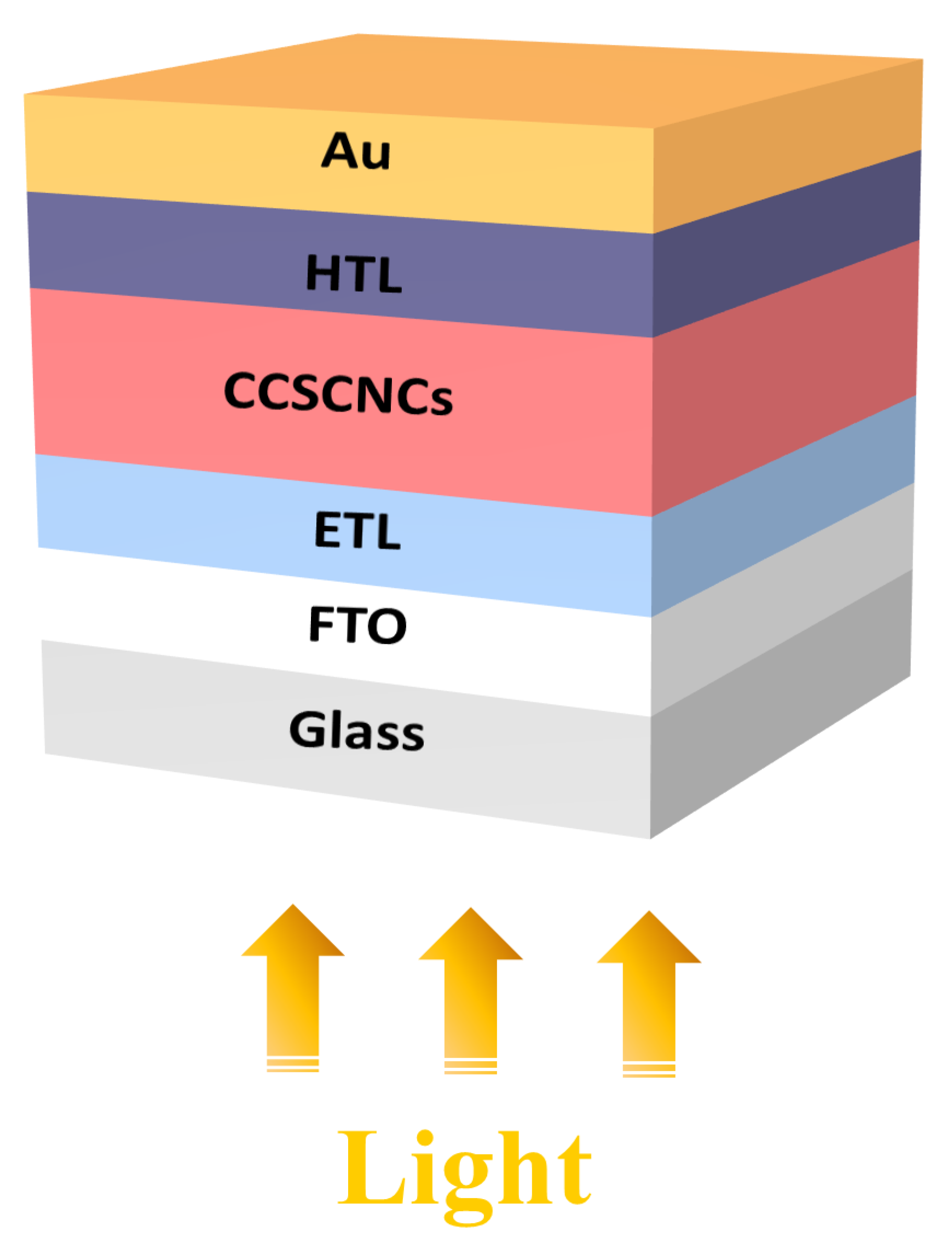
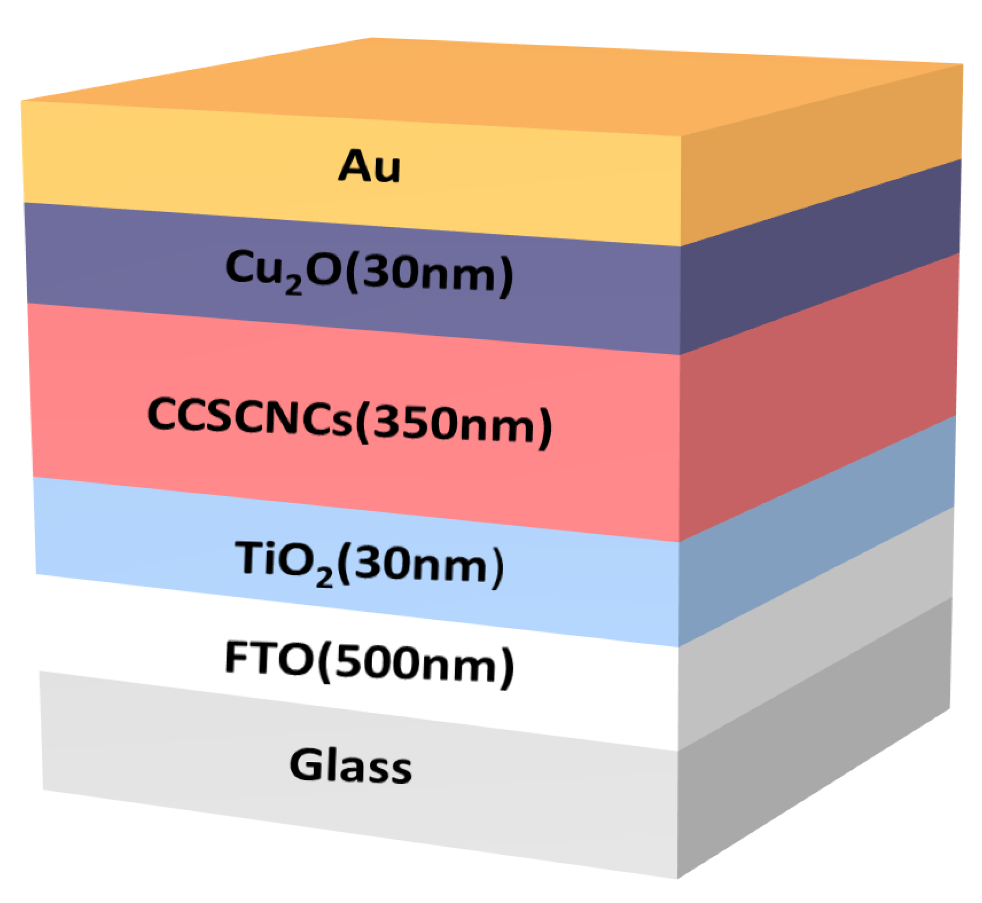
2.2. Device Structure and Materials
3. Results and Discussion
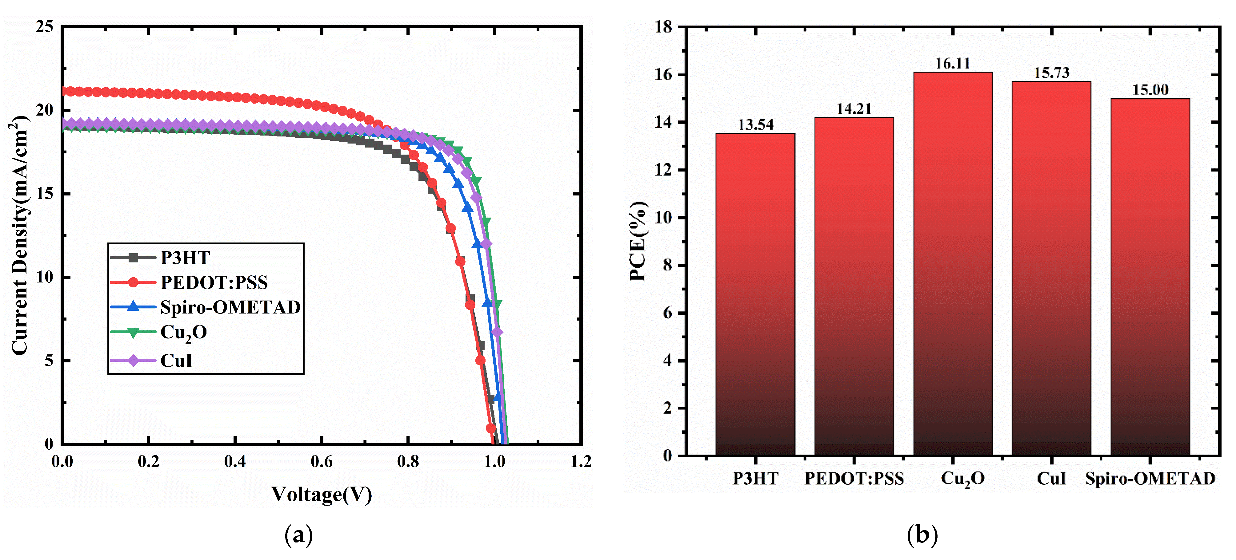
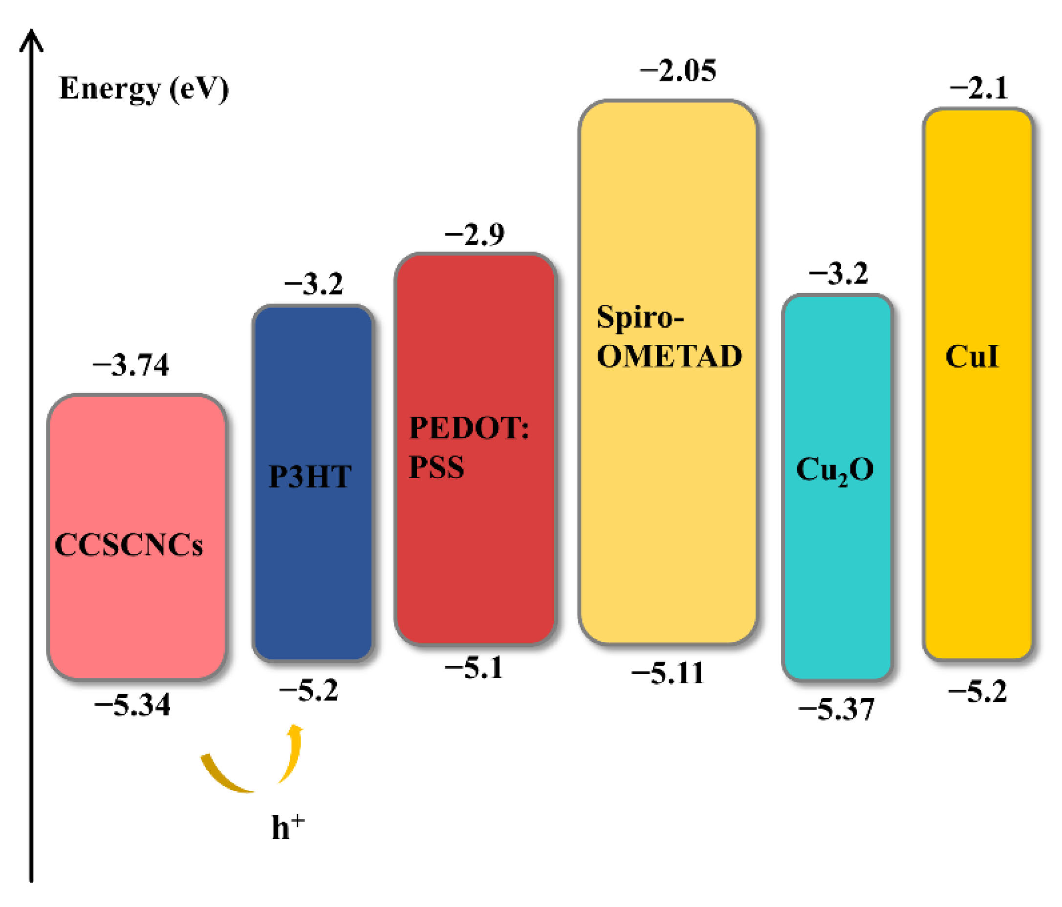
3.1. HTMs Selection
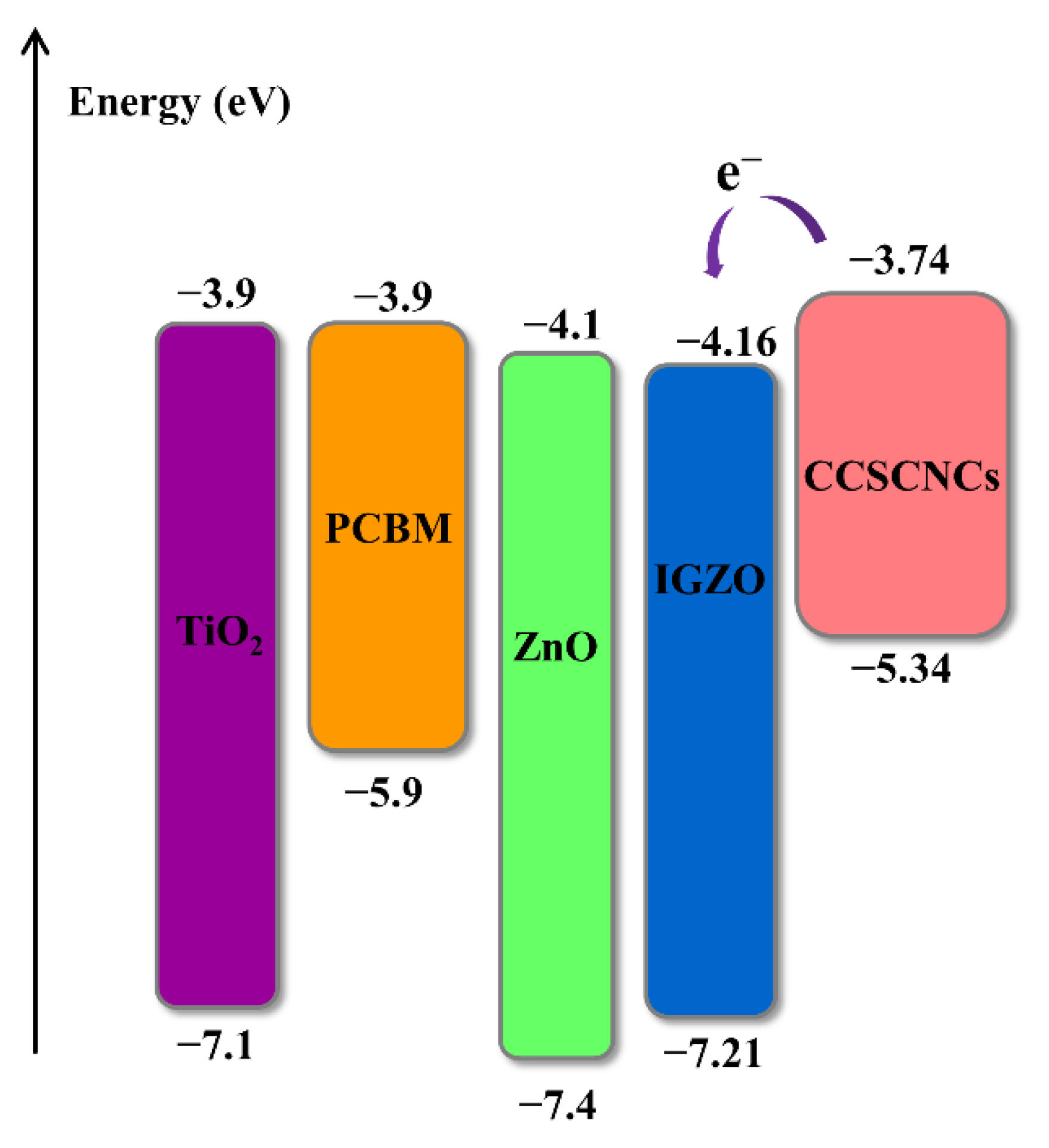
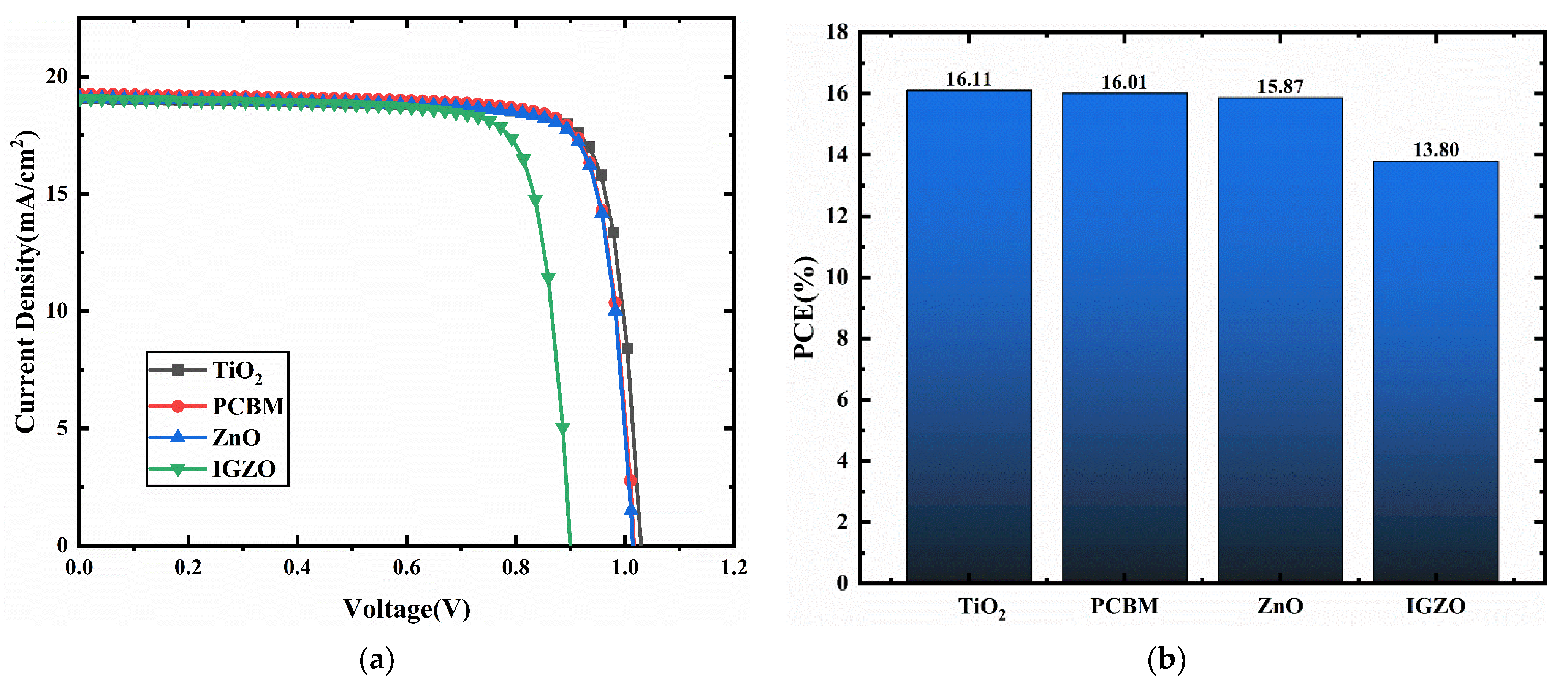
3.2. ETMs Selection
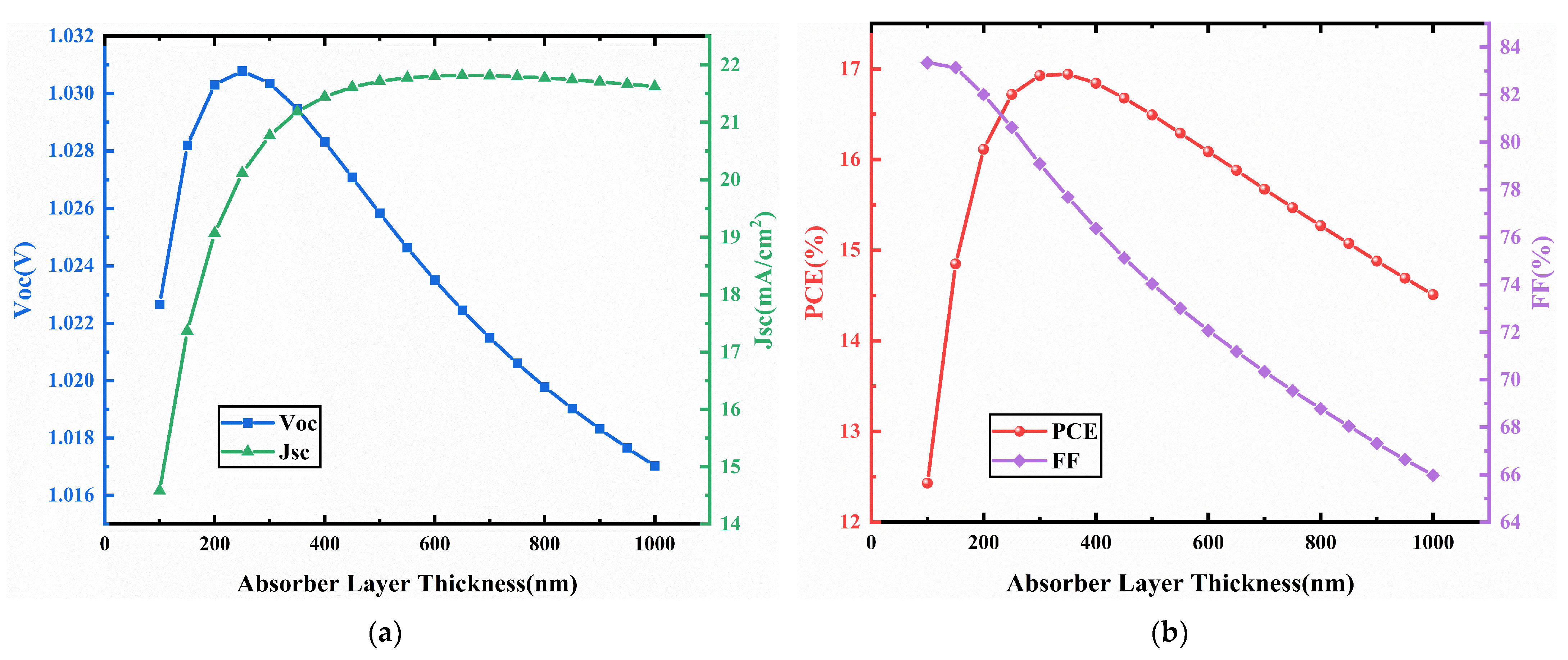
3.3. CCSCNC Thickness
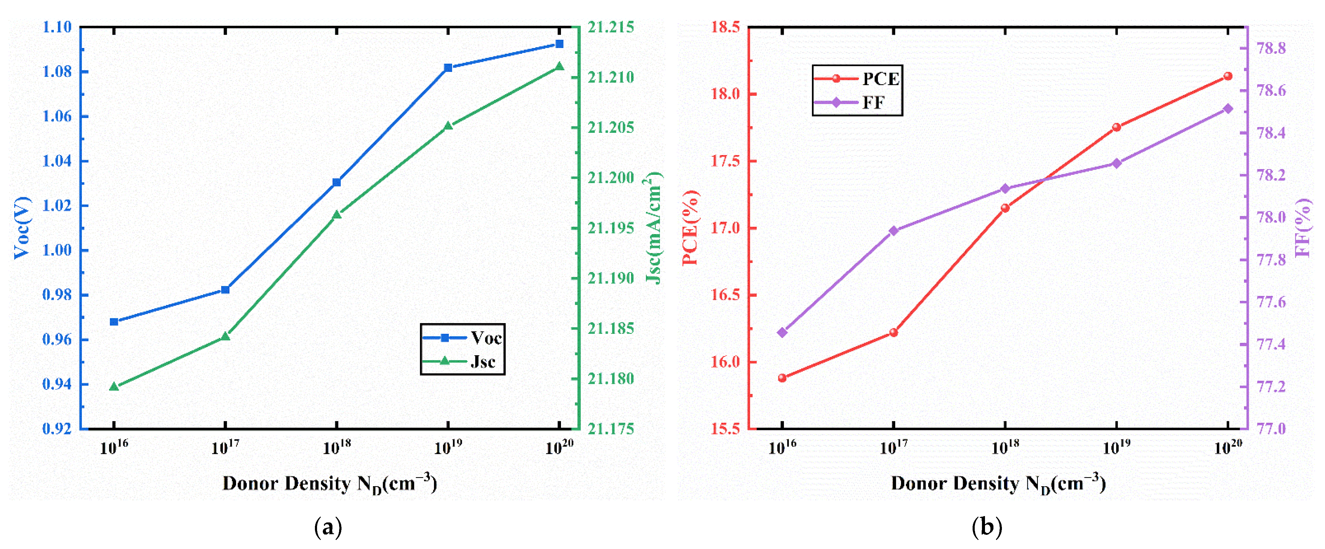
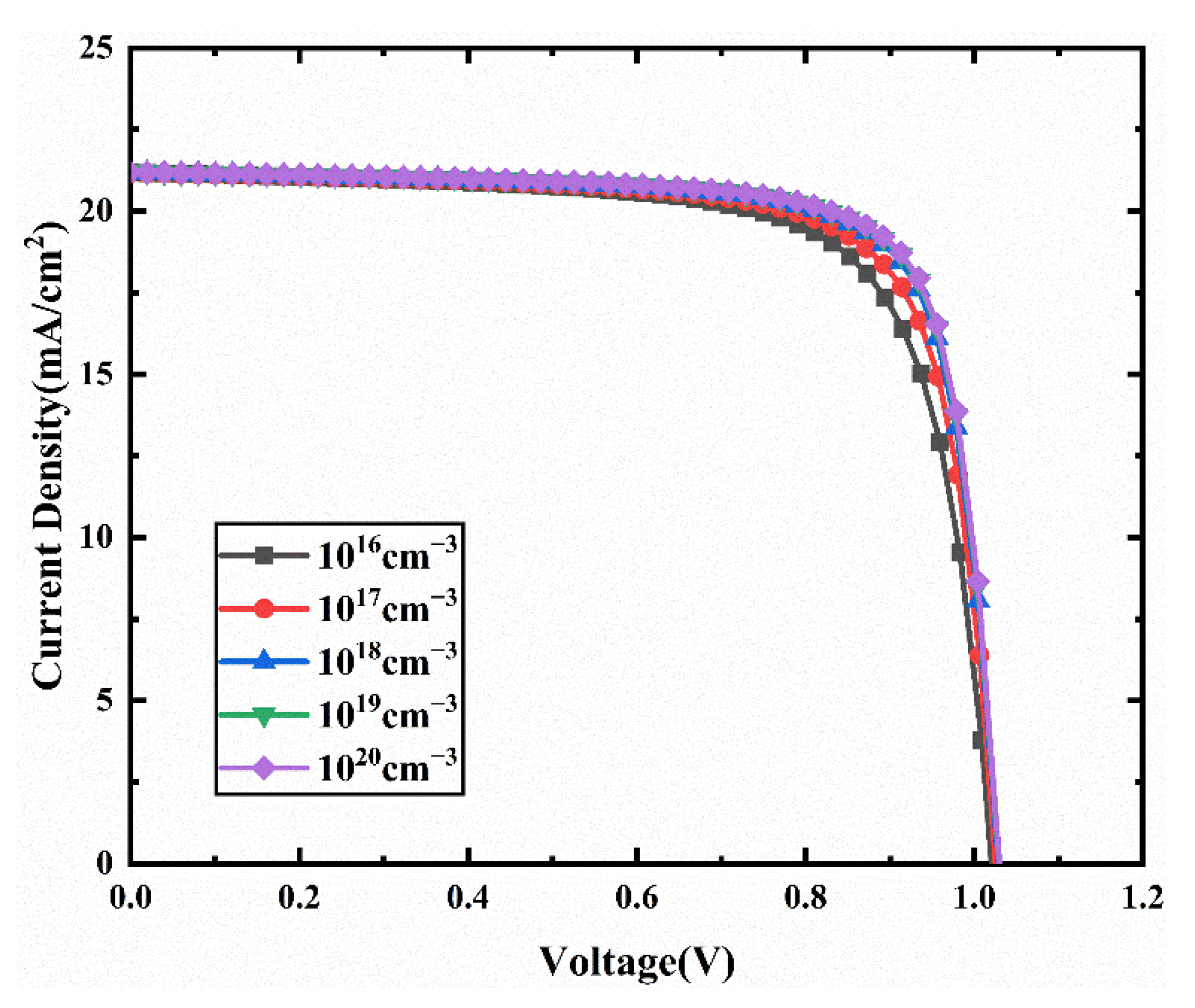
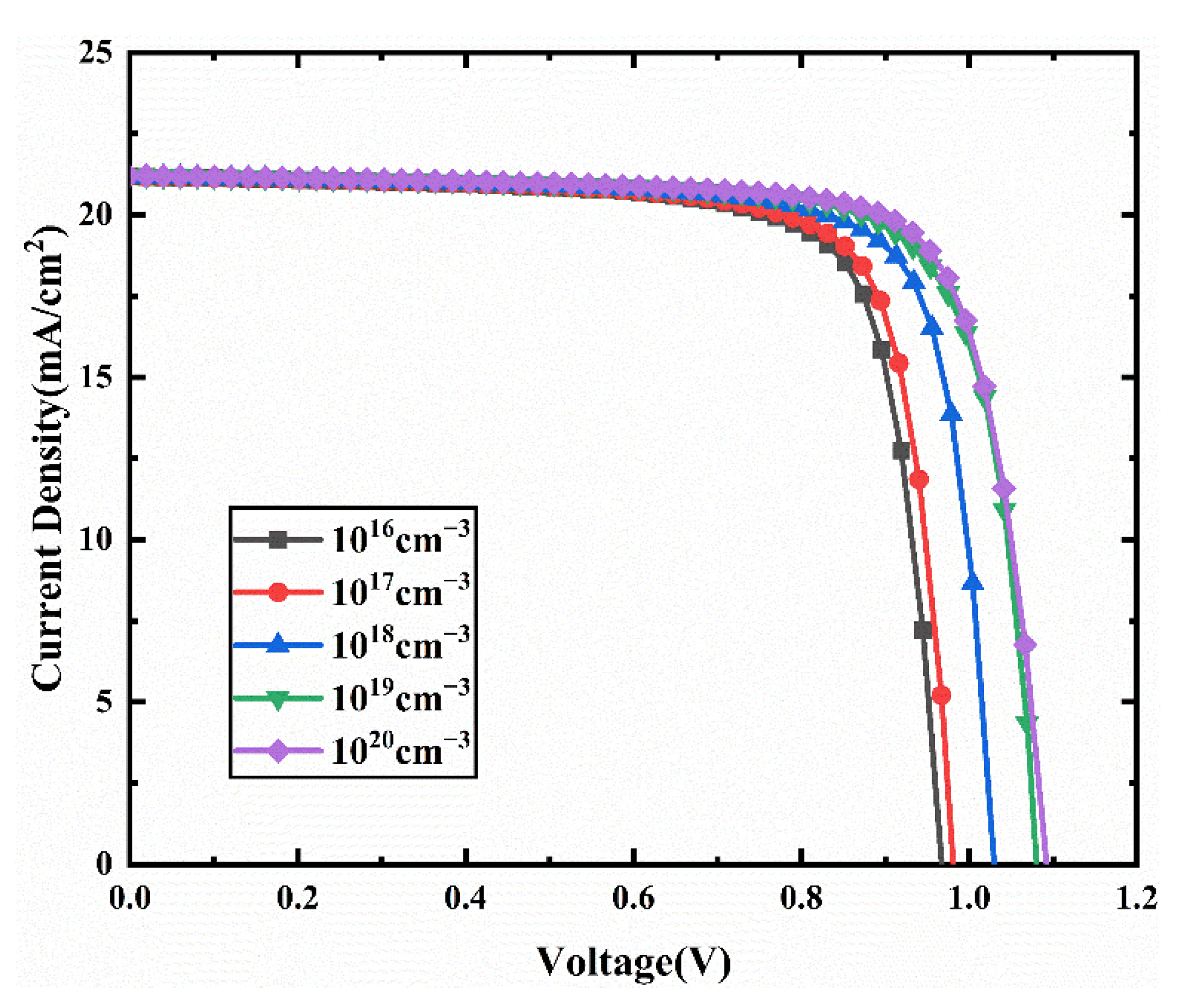
3.4. Effect of the Doping Density in the Transport Layers
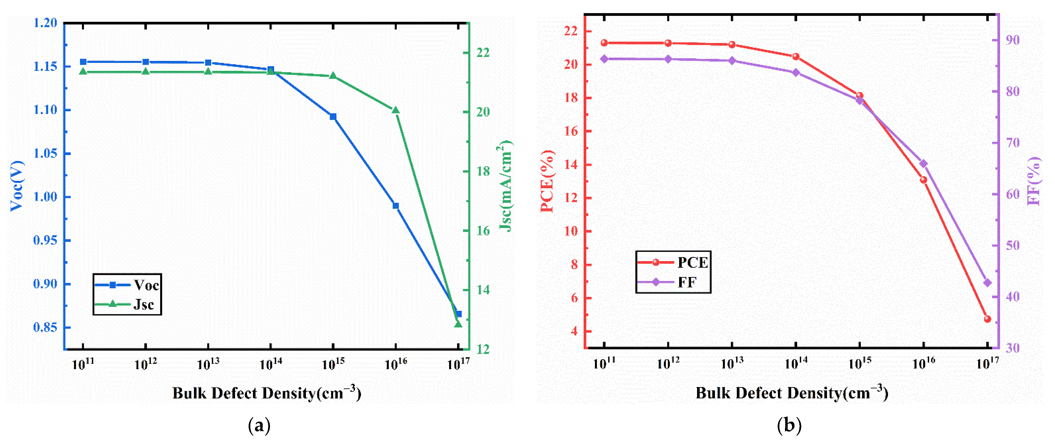
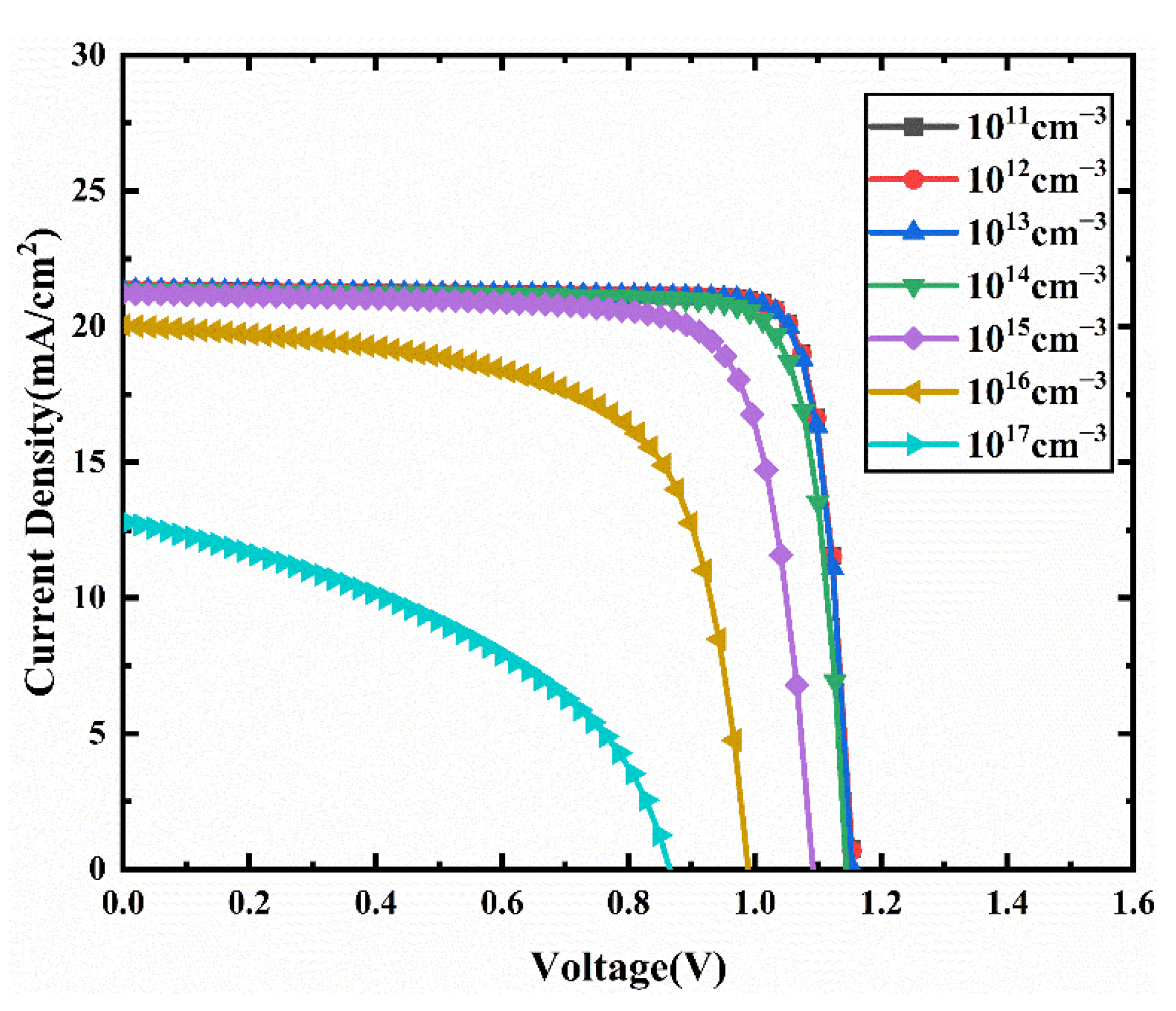
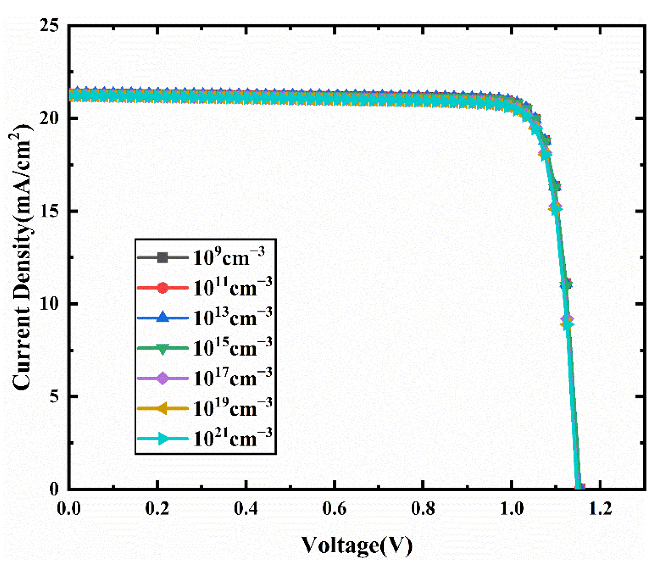
3.5. Effect of the Bulk Defect Density
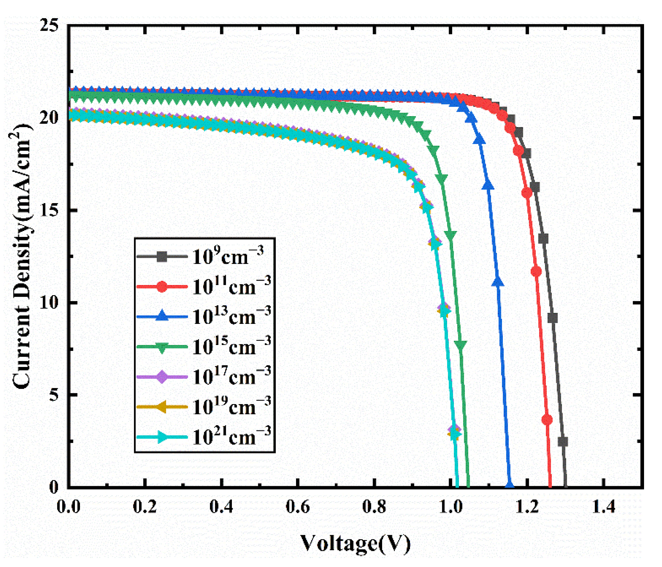
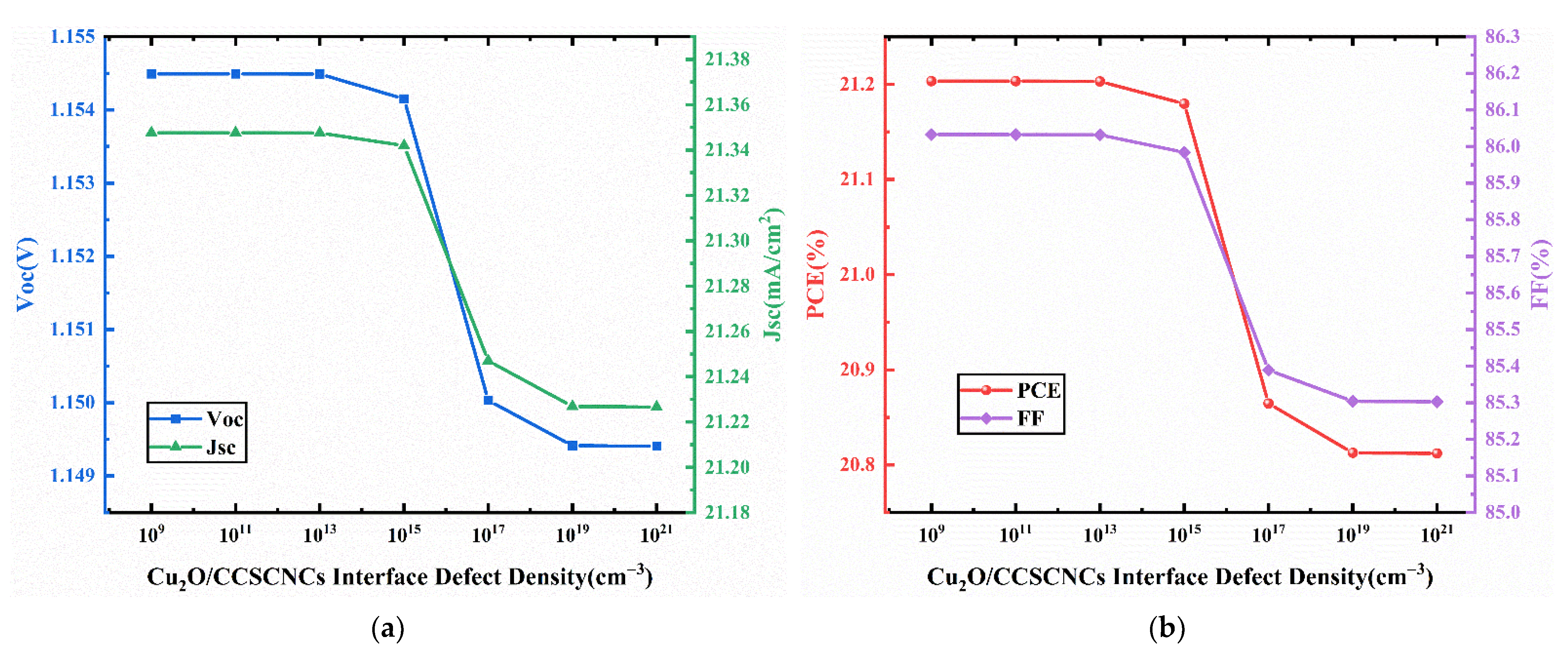
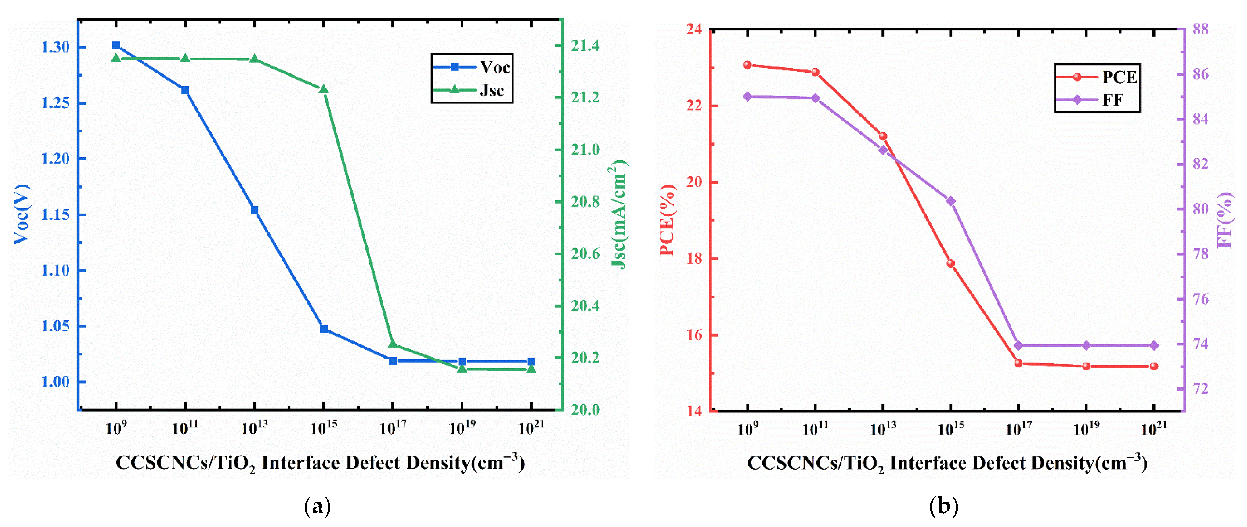
3.6. Effect of Interface Defect Density
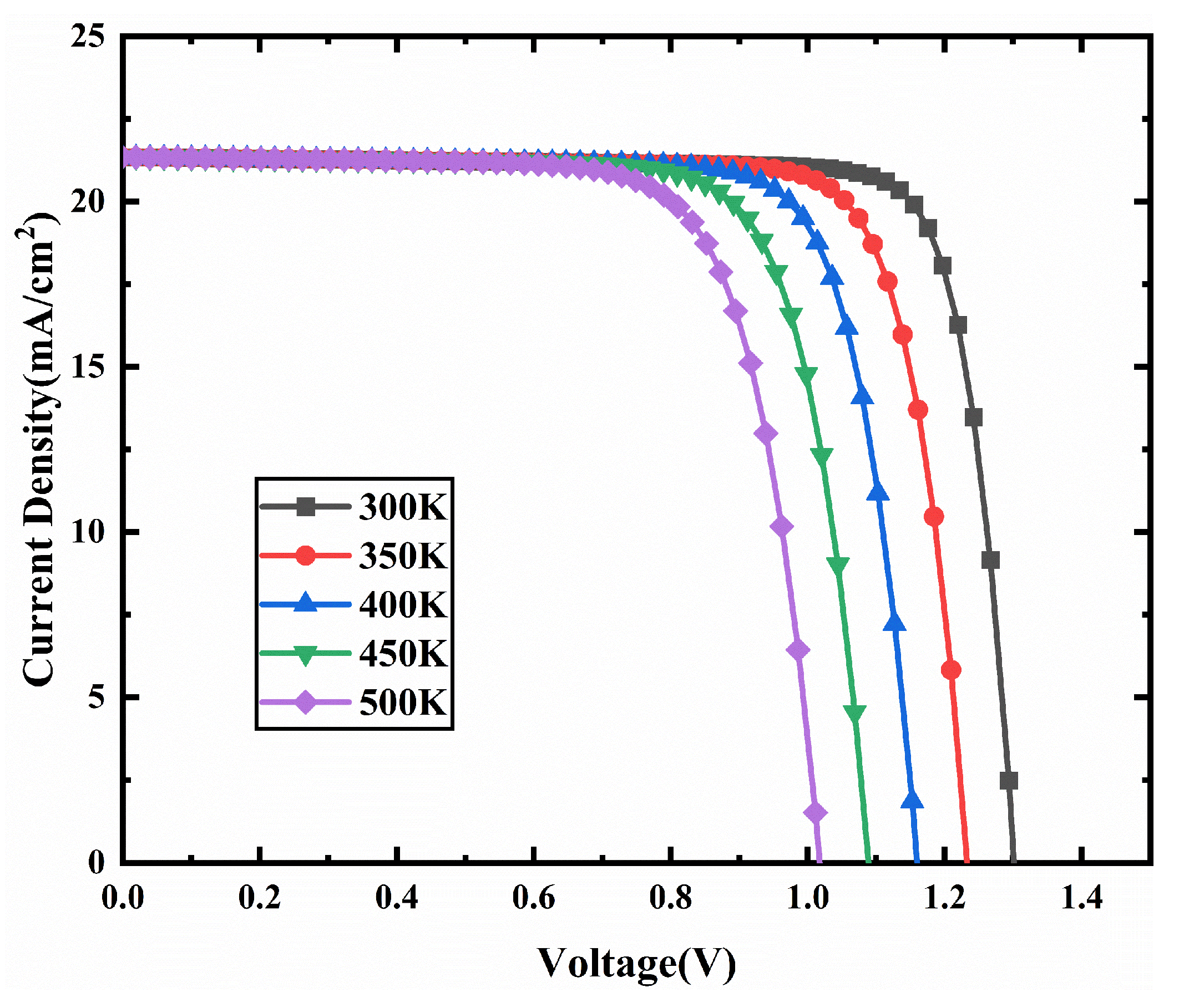
3.7. Effect of Operating Temperature
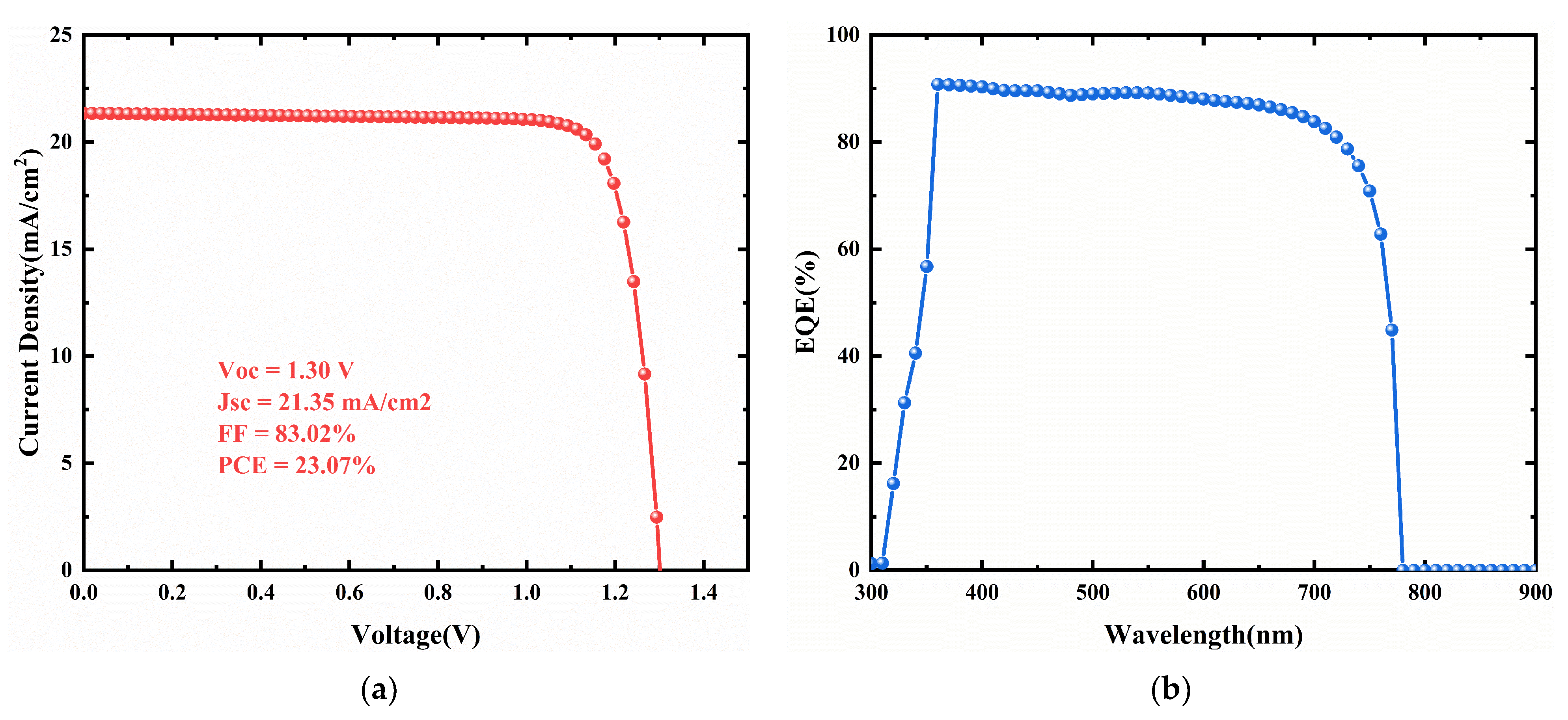
3.8. Performance with the Optimized Device Structure
4. Conclusions
Author Contributions
Funding
Data Availability Statement
Acknowledgments
Conflicts of Interest
References
- Kojima, A.; Teshima, K.; Shirai, Y.; Miyasaka, T. Organometal halide perovskites as visible-light sensitizers for photovoltaic cells. J. Am. Chem. Soc. 2009, 131, 6050–6051. [Google Scholar] [CrossRef]
- National Renewable Energy Laboratory. Perovskite Efficiency Chart; National Renewable Energy Laboratory: Golden, CO, USA, 2020. [Google Scholar]
- Zhang, T.; Li, H.; Ban, H.; Sun, Q.; Shen, Y.; Wang, M.K. Efficient CsSnI 3 -based inorganic perovskite solar cells based on a mesoscopic metal oxide framework via incorporating a donor element. J. Mater. Chem. A 2020, 8, 4118–4124. [Google Scholar] [CrossRef]
- Giustino, F.; Snaith, H.J. Toward lead-free perovskite solar cells. ACS Energy Lett. 2016, 1, 1233–1240. [Google Scholar] [CrossRef] [Green Version]
- Stranks, S.D.; Eperon, G.E.; Grancini, G.; Menelaou, C.; Alcocer, M.J.P.; Leijtens, T.; Herz, L.M.; Petrozza, A.; Snaith, H.J. Electron-Hole Diffusion Lengths Exceeding 1 Micrometer in an Organometal Trihalide Perovskite Absorber. Science 2013, 342, 341–344. [Google Scholar] [CrossRef] [PubMed] [Green Version]
- Yang, W.S.; Noh, J.H.; Jeon, N.J.; Kim, Y.C.; Ryu, S.; Seo, J.; Seok, S. High-performance photovoltaic perovskite layers fabricated through intramolecular exchange. Science 2015, 348, 1234–1237. [Google Scholar] [CrossRef]
- Yin, W.J.; Yang, J.H.; Kang, J.; Yan, Y.; Wei, S.H. Halide perovskite materials for solar cells: A theoretical review. J. Mater. Chem. A 2015, 3, 8926–8942. [Google Scholar] [CrossRef]
- Fabini, D.H.; Laurita, G.; Bechtel, J.S.; Stoumpos, C.C.; Evans, H.A.; Kontos, A.G.; Raptis, Y.S.; Falaras, P.; van der Ven, A.; Kanatzidis, M.G.; et al. Dynamic stereochemical activity of the Sn2+ lone pair in perovskite CsSnBr3. J. Am. Chem. Soc. 2016, 138, 11820–11832. [Google Scholar] [CrossRef] [Green Version]
- Shi, Z.; Guo, J.; Chen, Y.; Li, Q.; Pan, Y.; Zhang, H.; Xia, Y.; Huang, W. Lead-free organic–inorganic hybrid perovskites for photovoltaic applications: Recent advances and perspectives. Adv. Mater. 2017, 29, 1605005. [Google Scholar] [CrossRef]
- Krishnamoorthy, T.; Ding, H.; Yan, C.; Leong, W.L.; Baikie, T.; Zhang, Z.; Sherburne, M.; Li, S.; Asta, M.; Mathews, N.; et al. Lead-free germanium iodide perovskite materials for photovoltaic application. J. Mater. Chem. A 2015, 3, 23829–23832. [Google Scholar] [CrossRef]
- Pradhan, B.; Kumar, G.S.; Sain, S.; Dalui, A.; Ghorai, U.K.; Pradhan, S.K.; Acharya, S. Size tunable cesium antimony chloride perovskite nanowires and nanorods. Chem. Mater. 2018, 30, 2135–2142. [Google Scholar] [CrossRef]
- Pal, J.; Manna, S.; Mondal, A.; Das, S.; Adarsh, K.V.; Nag, A. Colloidal Synthesis and Photophysics of M3Sb2I9 (M = Cs and Rb) Nanocrystals: Lead-Free Perovskites. Angew. Chem. Int. Ed. 2017, 56, 14187–14191. [Google Scholar] [CrossRef]
- Yang, B.; Chen, J.; Hong, F.; Mao, X.; Zheng, K.; Yang, S.; Li, Y.; Pullerits, T.; Deng, W.; Han, K. Lead-free, air-stable all-inorganic cesium bismuth halide perovskite nanocrystals. Angew. Chem. Int. Ed. 2017, 56, 12471–12475. [Google Scholar] [CrossRef]
- Nelson, R.D.; Santra, K.; Wang, Y.; Hadi, A.; Petrich, J.W.; Panthani, M.G. Synthesis and optical properties of ordered-vacancy perovskite cesium bismuth halide nanocrystals. Chem. Commun. 2018, 54, 3640–3643. [Google Scholar] [CrossRef] [Green Version]
- Pal, J.; Bhunia, A.; Chakraborty, S.; Manna, S.; Das, S.; Dewan, A.; Datta, S.; Nag, A. Synthesis and Optical Properties of Colloidal M3Bi2I9 (M = Cs, Rb) Perovskite Nanocrystals. J. Phys. Chem. C. 2018, 122, 10643–10649. [Google Scholar] [CrossRef]
- Pan, W.; Wu, H.; Luo, J.; Deng, Z.; Ge, C.; Chen, C.; Jiang, X.; Yin, W.-J.; Niu, G.; Zhu, L.; et al. Cs2AgBiBr6 single-crystal X-ray detectors with a low detection limit. Nat. Photonics 2017, 11, 726–732. [Google Scholar] [CrossRef]
- Zhou, L.; Xu, Y.-F.; Chen, B.-X.; Kuang, D.-B.; Su, C.-Y. Synthesis and Photocatalytic Application of Stable Lead-Free Cs2AgBiBr6 Perovskite Nanocrystals. Small 2018, 14, 1703762. [Google Scholar] [CrossRef]
- McClure, E.T.; Ball, M.R.; Windl, W.; Woodward, P.M. Cs2AgBiX6 (X = Br, Cl): New Visible Light Absorbing, Lead-Free Halide Perovskite Semiconductors. Chem. Mater. 2016, 28, 1348–1354. [Google Scholar] [CrossRef]
- Vargas, B.; Ramos, E.; Perez-Gutierrez, E.; Alonso, J.C.; Solis Ibarra, D. A Direct Bandgap Copper–Antimony Halide Perovskite. J. Am. Chem. Soc. 2017, 139, 9116–9119. [Google Scholar] [CrossRef]
- Singhal, N.; Chakraborty, R.; Ghosh, P.; Nag, A. Low-Bandgap Cs4CuSb2Cl12 Layered Double Perovskite: Synthesis, Reversible Thermal Changes, and Magnetic Interaction. Chem. Asian J. 2018, 13, 2085–2092. [Google Scholar] [CrossRef]
- Tang, G.; Xiao, Z.; Hosono, H.; Kamiya, T.; Fang, D.; Hong, J. Layered Halide Double Perovskites Cs3+nM(II)nSb2X9+3n (M = Sn, Ge) for Photovoltaic Applications. J. Phys. Chem. Lett. 2017, 9, 43–48. [Google Scholar] [CrossRef]
- Samadi, M.; Sarikhani, N.; Zirak, M.; Zhang, H.; Zhang, H.L.; Moshfegh, A.Z. Group 6 transition metal dichalcogenide nanomaterials: Synthesis, applications and future perspectives. Nanoscale Horiz. 2018, 3, 90–204. [Google Scholar] [CrossRef] [PubMed]
- Bandurin, D.A.; Tyurnina, A.V.; Yu, G.L.; Mishchenko, A.; Zolyomi, V.; Morozov, S.V.; Kumar, R.K.; Gorbachev, R.V.; Kudrynskyi, Z.R.; Pezzini, S.; et al. High electron mobility, quantum Hall effect and anomalous optical response in atomically thin InSe. Nat. Nanotechnol. 2017, 12, 223–227. [Google Scholar] [CrossRef]
- Akkerman, Q.A.; Motti, S.G.; Srimath Kandada, A.R.; Mosconi, E.; D’Innocenzo, V.; Bertoni, G.; Marras, S.; Kamino, B.A.; Miranda, L.; de Angelis, F.; et al. Solution Synthesis Approach to Colloidal Cesium Lead Halide Perovskite Nanoplatelets with Monolayer-Level Thickness Control. J. Am. Chem. Soc. 2016, 138, 1010–1016. [Google Scholar] [CrossRef] [PubMed] [Green Version]
- Wang, X.D.; Miao, N.H.; Liao, J.F.; Li, W.Q.; Xie, Y.; Chen, J.; Sun, Z.M.; Chen, H.Y.; Kuang, D.B. The top-down synthesis of single-layered Cs4CuSb2Cl12 halide perovskite nanocrystals for photoelectrochemical application. Nanoscale 2019, 11, 5180–5187. [Google Scholar] [CrossRef]
- Cai, T.; Shi, W.; Hwang, S.; Kobbekaduwa, K.; Nagaoka, Y.; Yang, H.; Hills-Kimball, K.; Zhu, H.; Wang, J.; Wang, Z.; et al. Lead-free Cs4CuSb2Cl12 layered double perovskite nanocrystals. J. Am. Chem. Soc. 2020, 142, 11927–11936. [Google Scholar] [CrossRef]
- Ashtiha, P.P.; Joshi, M.; Verma, D.; Jadhav, S.; Roy Choudhury, A.; Jana, D. Layered Cs4CuSb2Cl12 Nanocrystals for Sunlight-Driven Photocatalytic Degradation of Pollutants. ACS Appl. Nano Mater. 2021, 4, 1305–1313. [Google Scholar] [CrossRef]
- Que, M.; Zhu, L.; Guo, Y.; Que, W.; Yun, S. Toward perovskite nanocrystalline solar cells: Progress and potential. J. Mater. Chem. C 2020, 8, 5321–5334. [Google Scholar] [CrossRef]
- Zhou, F.; Li, Z.; Chen, H.; Wang, Q.; Ding, L.; Jin, Z. Application of perovskite nanocrystals (NCs)/quantum dots (QDs) in solar cells. Nano Energy 2020, 73, 104757. [Google Scholar] [CrossRef]
- Hao, M.; Bai, Y.; Zeiske, S.; Ren, L.; Liu, J.; Yuan, J.; Zarrabi, N.; Cheng, N.; Ghasemi, M.; Chen, P.; et al. Ligand-assisted cation-exchange engineering for high-efficiency colloidal Cs1−xFAxPbI3 quantum dot solar cells with reduced phase segregation. Nat. Energy 2020, 5, 79–88. [Google Scholar] [CrossRef]
- Burgelman, M.; Nollet, P.; Degrave, S. Modelling polycrystalline semiconductor solar cells. Thin Solid Films 2000, 361, 527–532. [Google Scholar] [CrossRef]
- Trinh, M.T.; Wu, X.; Niesner, D.; Zhu, X.-Y. Many-body interactions in photo-excited lead iodide perovskite. J. Mater. Chem. A 2015, 3, 9285–9290. [Google Scholar] [CrossRef]
- Ahmed, S.; Jannat, F.; Khan, M.A.K.; Alim, M.A. Numerical development of eco-friendly Cs2TiBr6 based perovskite solar cell with all-inorganic charge transport materials via SCAPS-1D. Optik 2021, 225, 165765. [Google Scholar] [CrossRef]
- Jani, M.R.; Islam, M.T.; Amin, S.M.A.; Sami, M.S.U.; Shorowordi, K.M.; Hossain, M.I.; Chowdhury, S.; Nishat, S.S.; Ahmed, S. Exploring solar cell performance of inorganic Cs2TiBr6 halide double perovskite: A numerical study. Superlattice Microst. 2020, 146, 106652. [Google Scholar] [CrossRef]
- Chowdhury, M.S.; Shahahmadi, S.A.; Chelvanathan, P.; Tiong, S.K.; Amin, N.; Techato, K.; Nuthammachot, N.; Chowdhury, T.; Suklueng, M. Effect of deep-level defect density of the absorber layer and n/i interface in perovskite solar cells by SCAPS-1D. Results Phys. 2020, 16, 102839. [Google Scholar] [CrossRef]
- Karimi, E.; Ghorashi, S.M.B. Investigation of the influence of different hole-transporting materials on the performance of perovskite solar cells. Optik 2017, 130, 650–658. [Google Scholar] [CrossRef]
- Jayan, K.D.; Sebastian, V. Comprehensive device modelling and performance analysis of MASnI3 based perovskite solar cells with diverse ETM, HTM and back metal contacts. Solar Energy 2021, 217, 40–48. [Google Scholar] [CrossRef]
- Raj, A.; Anshul, A.; Tuli, V.; Singh, P.K.; Singh, R.C.; Kumar, M. Effect of appropriate ETL on quantum efficiency of double perovskite La2NiMnO6 based solar cell device via SCAPS simulation. Mater. Today Proc. 2021, in press. [Google Scholar] [CrossRef]
- Lakhdar, N.; Hima, A. Electron transport material effect on performance of perovskite solar cells based on CH3NH3GeI3. Opt. Mater. 2020, 99, 109517. [Google Scholar] [CrossRef]
- Islam, S.; Sobayel, K.; Al-Kahtani, A.; Islam, M.A.; Muhammad, G.; Amin, N.; Shahiduzzaman, M.; Akhtaruzzaman, M. Defect Study and Modelling of SnX3-Based Perovskite Solar Cells with SCAPS-1D. Nanomaterials 2021, 11, 1218. [Google Scholar] [CrossRef]
- Tanaka, K.; Minemoto, T.; Takakura, H. Analysis of heterointerface recombination by Zn1− xMgxO for window layer of Cu (In, Ga) Se2 solar cells. Solar Energy 2009, 83, 477–479. [Google Scholar] [CrossRef]
- Turcu, M.; Rau, U. Fermi level pinning at CdS/Cu(In,Ga)(Se,S)2 interfaces: Effect of chalcopyrite alloy composition. J. Phys. Chem. Solids 2003, 64, 1591–1595. [Google Scholar] [CrossRef]
- Gan, Y.; Bi, X.; Liu, Y.; Qin, B.; Li, Q.; Jiang, Q.; Mo, P. Numerical investigation energy conversion performance of tin-based perovskite solar cells using cell capacitance simulator. Energies 2020, 13, 5907. [Google Scholar] [CrossRef]
- Tan, K.; Lin, P.; Wang, G.; Liu, Y.; Xu, Z.; Lin, Y. Controllable design of solid-state perovskite solar cells by SCAPS device simulation. Solid-State Electron. 2016, 126, 75–80. [Google Scholar] [CrossRef]
- Khoshsirat, N.; Yunus, N.A.M.; Hamidon, M.N.; Shafie, S.; Amin, N. Analysis of absorber layer properties effect on CIGS solar cell performance using SCAPS. Optik 2015, 126, 681–686. [Google Scholar] [CrossRef]
- Abate, A.; Leijtens, T.; Pathak, S.; Teuscher, J.; Avolio, R.; Errico, M.E.; Kirkpatrik, J.; Ball, J.M.; Docampo, P.; McPhersonc, I.; et al. Lithium salts as “redox active” p-type dopants for organic semiconductors and their impact in solid-state dye-sensitized solar cells. Phys. Chem. Chem. Phys. 2013, 15, 2572–2579. [Google Scholar] [CrossRef] [PubMed]
- Leijtens, T.; Lim, J.; Teuscher, J.; Park, T.; Snaith, H.J. Charge density dependent mobility of organic hole-transporters and mesoporous TiO2 determined by transient mobility spectroscopy: Implications to dye-sensitized and organic solar cells. Adv. Mater. 2013, 25, 3227–3233. [Google Scholar] [CrossRef]
- Trukhanov, V.A.; Bruevich, V.V.; Paraschuk, D.Y. Effect of doping on performance of organic solar cells. Phys. Rev. B 2011, 84, 205–318. [Google Scholar] [CrossRef] [Green Version]
- Ghadiri, M.; Kang, A.K.; Gorji, N.E. XRD characterization of graphene-contacted perovskite solar cells: Moisture degradation and dark-resting recovery. Superlattices Microstruct. 2020, 146, 106677. [Google Scholar] [CrossRef]
- Huang, L.; Sun, X.; Li, C.; Xu, R.; Xu, J.; Du, Y.; Wu, Y.; Ni, J.; Cai, H.; Li, J.; et al. Electron transport layer-free planar perovskite solar cells: Further performance enhancement perspective from device simulation. Sol. Energy Mater. Sol. Cells 2016, 157, 1038–1047. [Google Scholar] [CrossRef]
- Lin, L.; Li, P.; Jiang, L.; Kang, Z.; Yan, Q.; Xiong, H.; Lien, S.; Zhang, P.; Qiu, Y. Boosting efficiency up to 25% for HTL-free carbon-based perovskite solar cells by gradient doping using SCAPS simulation. Sol. Energy 2021, 215, 328–334. [Google Scholar] [CrossRef]
- Slami, A.; Bouchaour, M.; Merad, L. Comparative study of modelling of Perovskite solar cell with different HTM layers. Int. J. Mater. 2020, 7, 2313–10555. [Google Scholar] [CrossRef]
- Devi, N.; Parrey, K.A.; Aziz, A.; Datta, S. Numerical simulations of perovskite thin-film solar cells using a CdS hole blocking layer. J. Vac. Sci. Technol. B 2018, 36, 04G105. [Google Scholar] [CrossRef]
- Behrouznejad, F.; Shahbazi, S.; Taghavinia, N.; Wu, H.-P.; Wei-Guang Diau, E. A study on utilizing different metals as the back contact of CH 3 NH 3 PbI 3 perovskite solar cells. J. Mater. Chem. A 2016, 4, 13488–13498. [Google Scholar] [CrossRef]
- Chakraborty, K.; Choudhury, M.G.; Paul, S. Study of Physical, Optical, and Electrical Properties of Cesium Titanium (IV)-Based Single Halide Perovskite Solar Cell. IEEE J. Photovolt. 2021, 11, 386–390. [Google Scholar] [CrossRef]
- Singh, A.K.; Srivastava, S.; Mahapatra, A.; Baral, J.K.; Pradhan, B. Performance optimization of lead free-MASnI3 based solar cell with 27% efficiency by numerical simulation. Opt. Mater. 2021, 117, 111193. [Google Scholar] [CrossRef]
- Kumar, M.; Raj, A.; Kumar, A.; Anshul, A. An optimized lead-free formamidinium Sn-based perovskite solar cell design for high power conversion efficiency by SCAPS simulation. Opt. Mater. 2020, 108, 110213. [Google Scholar] [CrossRef]
- Khattak, Y.H.; Baig, F.; Shuja, A.; Beg, S.; Soucase, B.M. Numerical analysis guidelines for the design of efficient novel nip structures for perovskite solar cell. Sol. Energy 2020, 207, 579–591. [Google Scholar] [CrossRef]
- Coulibaly, A.B.; Oyedele, S.O.; Kre, N.A.; Aka, B. Comparative study of lead-free perovskite solar cells using different hole transporter materials. Model. Numer. Simul. Mater. Sci. 2019, 9, 97–107. [Google Scholar] [CrossRef] [Green Version]
- Ahmad, O.; Rashid, A.; Ahmed, M.W.; Nasir, M.F.; Qasim, I. Performance evaluation of Au/p-CdTe/Cs2TiI6/n-TiO2/ITO solar cell using SCAPS-1D. Opt. Mater. 2021, 117, 111105. [Google Scholar] [CrossRef]


| Parameters | CCSCNCs | P3HT | PEDOT:PSS | Spiro-OMETAD | Cu2O | CuI |
|---|---|---|---|---|---|---|
| Thickness, d (nm) | 200 | 30 | 30 | 30 | 30 | 30 |
| Band gap, Eg (eV) | 1.6 | 2 | 2.2 | 3.06 | 2.17 | 3.1 |
| Electron affinity, χ (eV) | 3.74 | 3.2 | 2.9 | 2.05 | 3.2 | 2.1 |
| Permittivity, εr | 10 | 3 | 3 | 3 | 7.1 | 6.5 |
| Effective density states at CB, NC (cm−3) | 4.5 × 10¹⁸ | 1 × 10²⁰ | 2.2 × 10¹⁵ | 2.8 × 10¹⁹ | 2.5 × 10¹⁸ | 2.2 × 10¹⁹ |
| Effective density states at VB, NV (cm−3) | 1.6 × 10¹⁸ | 1 × 10²⁰ | 1.8 × 10¹⁸ | 1 × 10¹⁹ | 1.8 × 10¹⁹ | 1.8 × 10¹⁹ |
| Electron mobility, μn (cm−2/V·s) | 2.5 | 0.0001 | 10 | 1× 10⁻⁴ | 200 | 100 |
| Hole mobility, μp (cm−2/V·s) | 2.5 | 0.0001 | 10 | 2× 10⁻⁴ | 80 | 43.9 |
| Density of n-type doping, ND (cm−3) | 1 × 10¹³ | 0 | 0 | 0 | 0 | 0 |
| Density of p-type doping, NA (cm−3) | 1 × 10¹³ | 1 × 10¹⁶ | 3.17 × 10¹⁴ | 1 × 10¹⁸ | 9.1 × 10²¹ | 1 × 10¹⁸ |
| Defect density, Nt (cm−3) | 1 × 10¹⁵ | 1 × 10¹⁵ | 1 × 10¹⁴ | 1 × 10¹⁴ | 1 × 10¹⁴ | 1 × 10¹⁴ |
| electron thermal velocity (cm/s) | 1 × 10⁷ | 1 × 10⁷ | 1 × 10⁷ | 1 × 10⁷ | 1 × 10⁷ | 1 × 10⁷ |
| hole thermal velocity (cm/s) | 1 × 10⁷ | 1 × 10⁷ | 1 × 10⁷ | 1 × 10⁷ | 1 × 10⁷ | 1 × 10⁷ |
| Capture cross-section electrons (cm2) | 1 × 10⁻¹⁴ | 1 × 10⁻¹⁵ | 1 × 10⁻¹⁵ | 1 × 10⁻¹⁵ | 1 × 10⁻¹⁵ | 1 × 10⁻¹⁵ |
| Capture cross-section holes (cm2) | 1 × 10⁻¹⁴ | 1 × 10⁻¹⁵ | 1 × 10⁻¹⁵ | 1 × 10⁻¹⁵ | 1 × 10⁻¹⁵ | 1 × 10⁻¹⁵ |
| Reference | [19,20,21,25,26,32,33,34,37,40] | [33] | [35] | [36] | [34] | [38] |
| Parameters | TiO2 | PCBM | ZnO | IGZO |
|---|---|---|---|---|
| Thickness, d (nm) | 30 | 30 | 30 | 30 |
| Band gap, Eg (eV) | 3.2 | 2 | 3.3 | 3.05 |
| Electron affinity, χ (eV) | 4.1 | 3.9 | 4.1 | 4.16 |
| Permittivity, εr | 9 | 3.9 | 9 | 10 |
| Effective density states at CB NC (cm−3) | 2.2 × 10¹⁸ | 2.5 × 10²¹ | 4 × 10¹⁸ | 5 × 10¹⁸ |
| Effective density states at VB NV (cm−3) | 1 × 10¹⁹ | 2.5 × 10²¹ | 1 × 10¹⁹ | 1 × 10¹⁸ |
| Electron mobility, μn (cm−2/V·s) | 20 | 0.2 | 100 | 15 |
| Hole mobility, μp (cm−2/V·s) | 10 | 0.2 | 25 | 0.2 |
| Density of n-type doping, ND (cm−3) | 1 × 10¹⁸ | 2.93 × 10¹⁷ | 1 × 10¹⁸ | 1 × 10¹⁷ |
| Density of p-type doping, NA (cm−3) | 0 | 0 | 1 × 10⁵ | 0 |
| Defect density, Nt (cm−3) | 1 × 10¹⁵ | 1 × 10¹⁵ | 2 × 10¹⁷ | 1 × 10¹⁵ |
| electron thermal velocity (cm/s) | 1 × 10⁷ | 1 × 10⁷ | 1 × 10⁷ | 1 × 10⁷ |
| hole thermal velocity (cm/s) | 1 × 10⁷ | 1 × 10⁷ | 1 × 10⁷ | 1 × 10⁷ |
| Capture cross-section electrons (cm2) | 2 × 10⁻¹⁴ | 1 × 10⁻¹⁵ | 1 × 10⁻¹⁵ | 2 × 10⁻¹⁴ |
| Capture cross-section holes (cm2) | 2 × 10⁻¹⁴ | 1 × 10⁻¹⁵ | 1 × 10⁻¹⁵ | 2 × 10⁻¹⁴ |
| Reference | [33] | [38] | [39] | [37] |
| Parameters | ETL/Absorber | Absorber/HTL | CCSCNCs |
|---|---|---|---|
| Defect type | Neutral | Neutral | Neutral |
| Capture cross-section for electrons (cm2) | 1 × 10⁻¹⁹ | 1 × 10⁻¹⁸ | 1 × 10⁻¹⁵ |
| Capture cross-section for holes (cm2) | 1 × 10⁻¹⁸ | 1 × 10⁻¹⁹ | 1 × 10⁻¹⁵ |
| Energetic distribution | Gaussian | Gaussian | Gaussian |
| Energy level with respect to Ev | 0.6 | 0.6 | 0.6 |
| Characteristic energy (eV) | 0.1 | 0.1 | 0.1 |
| Total density (cm−3) | 1 × 10¹³ | 1 × 10¹³ | 1 × 10¹⁵ |
| Reference | [33] | [33] | [33,40] |
| Hole Transport Material | Voc (V) | Jsc (mA/cm2) | FF (%) | PCE (%) |
|---|---|---|---|---|
| P3HT | 1.01 | 19.07 | 70.47 | 13.54 |
| PEDOT:PSS | 1.00 | 21.14 | 67.44 | 14.21 |
| Spiro-OMETAD | 1.02 | 19.21 | 76.54 | 15.00 |
| Cu2O | 1.03 | 19.07 | 82.01 | 16.11 |
| CuI | 1.03 | 19.22 | 79.66 | 15.73 |
| Electron Transport Material | Voc (V) | Jsc (mA/cm2) | FF (%) | PCE (%) |
|---|---|---|---|---|
| TiO2 | 1.03 | 19.07 | 82.01 | 16.11 |
| PCBM | 1.02 | 19.25 | 81.74 | 16.01 |
| ZnO | 1.02 | 19.07 | 81.97 | 15.87 |
| IGZO | 0.90 | 19.06 | 80.35 | 13.80 |
| Electron Transport Material | Voc (V) | Jsc (mA/cm2) | FF (%) | PCE (%) | Form | Ref |
|---|---|---|---|---|---|---|
| Cs2TiBr6 | 1.9 | 19.88 | 35.95 | 13.57 | simulation | [55] |
| Cs2TiI6 | 1.74 | 22.74 | 41 | 16.31 | simulation | [55] |
| MASnI3 | 1.203 | 25.97 | 87.79 | 27.43 | simulation | [56] |
| MASnI3 | 0.96 | 32.48 | 76.4 | 23.86 | simulation | [43] |
| FASnI3 | 1.81 | 31.2 | 33.72 | 19.08 | simulation | [57] |
| MASnBr3 | 0.8 | 31.88 | 84.89 | 21.66 | simulation | [55] |
| MAPbI3 | - | - | - | 25.15 | simulation | [51] |
| MAPbI3 | 1.05 | 24.48 | 86.31 | 26.96 | simulation | [58] |
| MASnI3 | 0.84 | 40.05 | 70.82 | 23.76 | simulation | [59] |
| Cs2TiI6 | 1.39 | 25.08 | 43.17 | 15.06 | simulation | [60] |
| Cs4CuSb2Cl12 nanocrystals | 1.30 | 21.35 | 83.02 | 23.07 | simulation | This work |
Publisher’s Note: MDPI stays neutral with regard to jurisdictional claims in published maps and institutional affiliations. |
© 2021 by the authors. Licensee MDPI, Basel, Switzerland. This article is an open access article distributed under the terms and conditions of the Creative Commons Attribution (CC BY) license (https://creativecommons.org/licenses/by/4.0/).
Share and Cite
He, Y.; Xu, L.; Yang, C.; Guo, X.; Li, S. Design and Numerical Investigation of a Lead-Free Inorganic Layered Double Perovskite Cs4CuSb2Cl12 Nanocrystal Solar Cell by SCAPS-1D. Nanomaterials 2021, 11, 2321. https://doi.org/10.3390/nano11092321
He Y, Xu L, Yang C, Guo X, Li S. Design and Numerical Investigation of a Lead-Free Inorganic Layered Double Perovskite Cs4CuSb2Cl12 Nanocrystal Solar Cell by SCAPS-1D. Nanomaterials. 2021; 11(9):2321. https://doi.org/10.3390/nano11092321
Chicago/Turabian StyleHe, Yizhou, Liyifei Xu, Cheng Yang, Xiaowei Guo, and Shaorong Li. 2021. "Design and Numerical Investigation of a Lead-Free Inorganic Layered Double Perovskite Cs4CuSb2Cl12 Nanocrystal Solar Cell by SCAPS-1D" Nanomaterials 11, no. 9: 2321. https://doi.org/10.3390/nano11092321
APA StyleHe, Y., Xu, L., Yang, C., Guo, X., & Li, S. (2021). Design and Numerical Investigation of a Lead-Free Inorganic Layered Double Perovskite Cs4CuSb2Cl12 Nanocrystal Solar Cell by SCAPS-1D. Nanomaterials, 11(9), 2321. https://doi.org/10.3390/nano11092321