
Silicon Metalens Fabrication from Electron Beam to UV-Nanoimprint Lithography

 ,
,  , , , , , , ,
Abstract
:1. Introduction
2. Materials and Methods
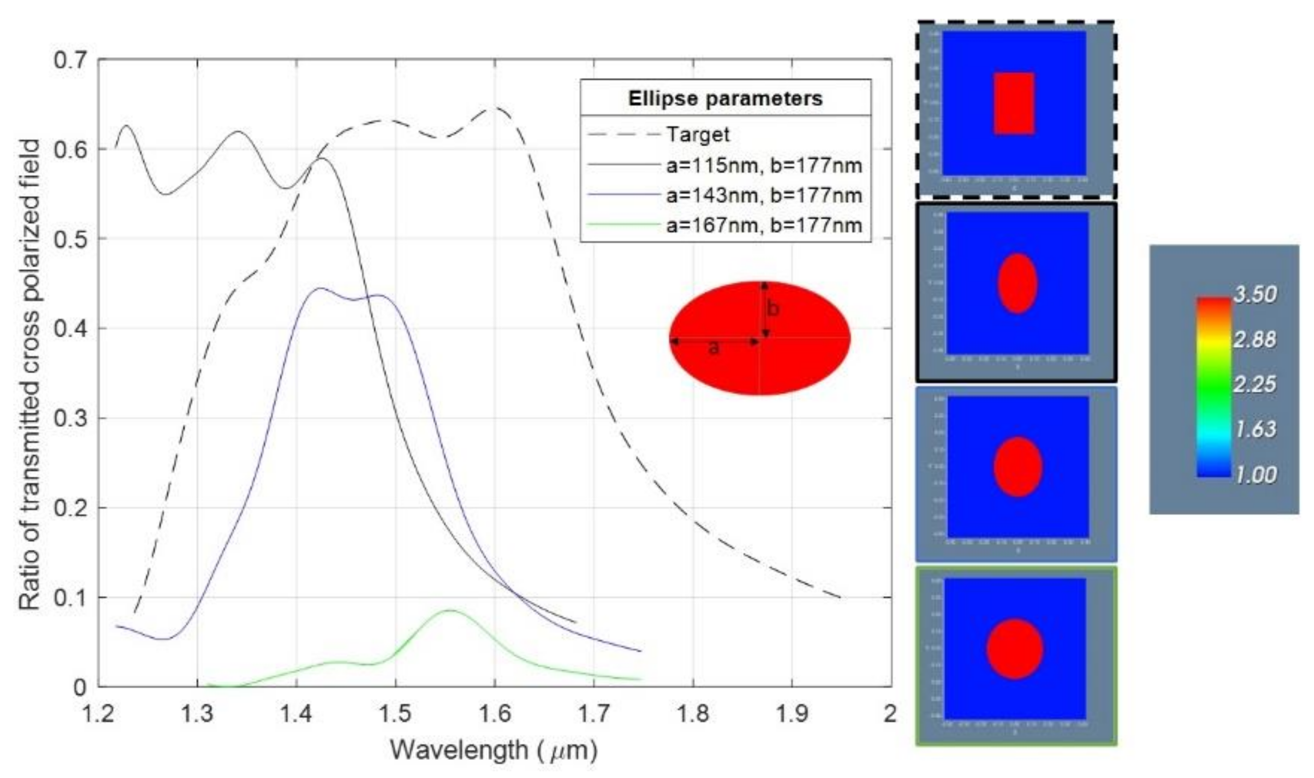
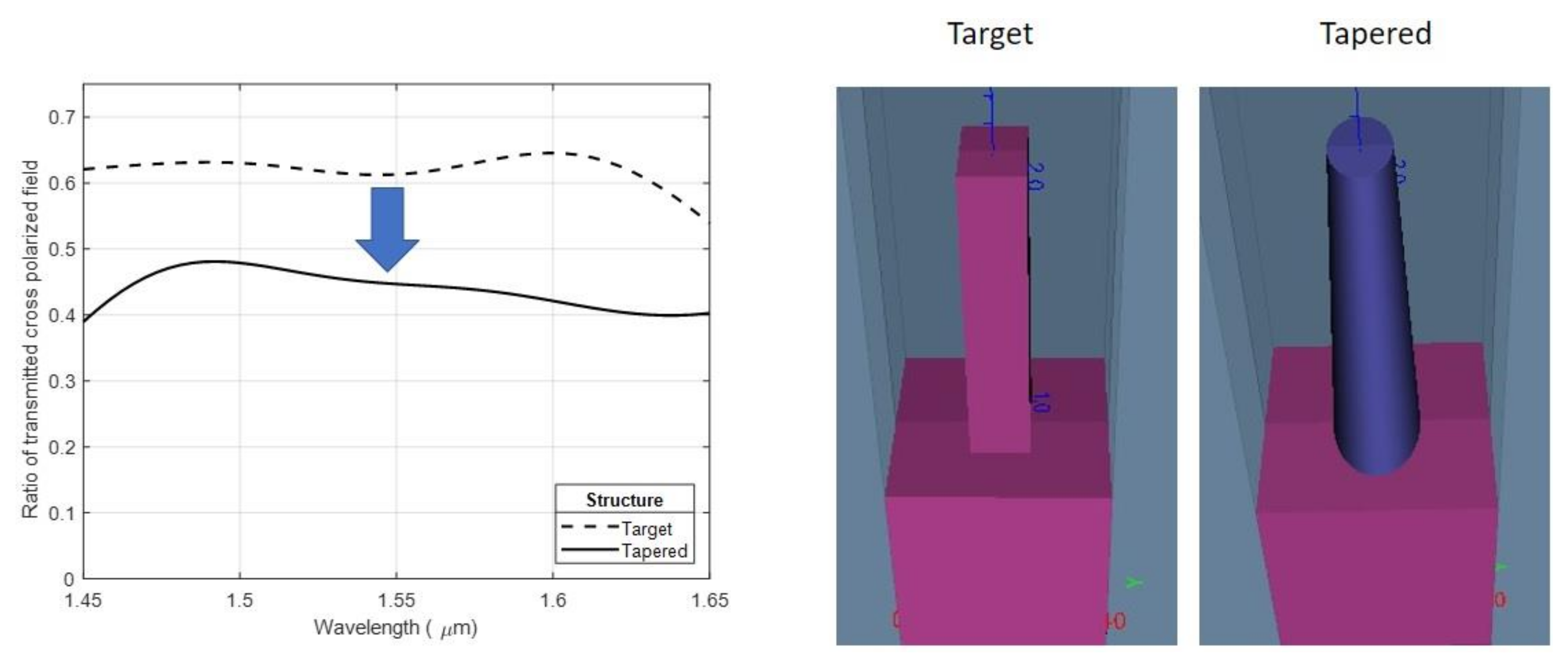
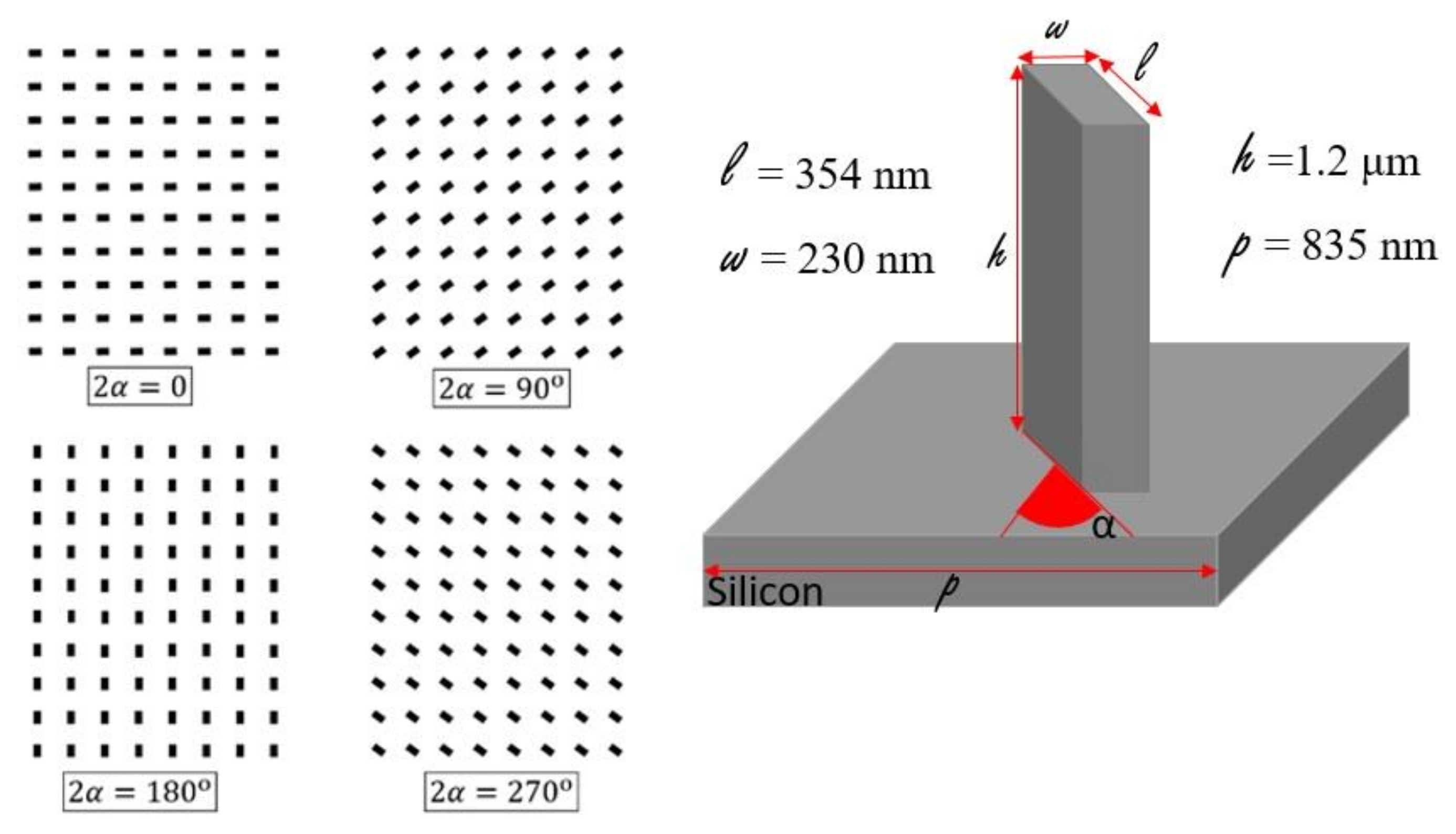
2.1. Lens Design Methodology
2.2. Experimental Approach
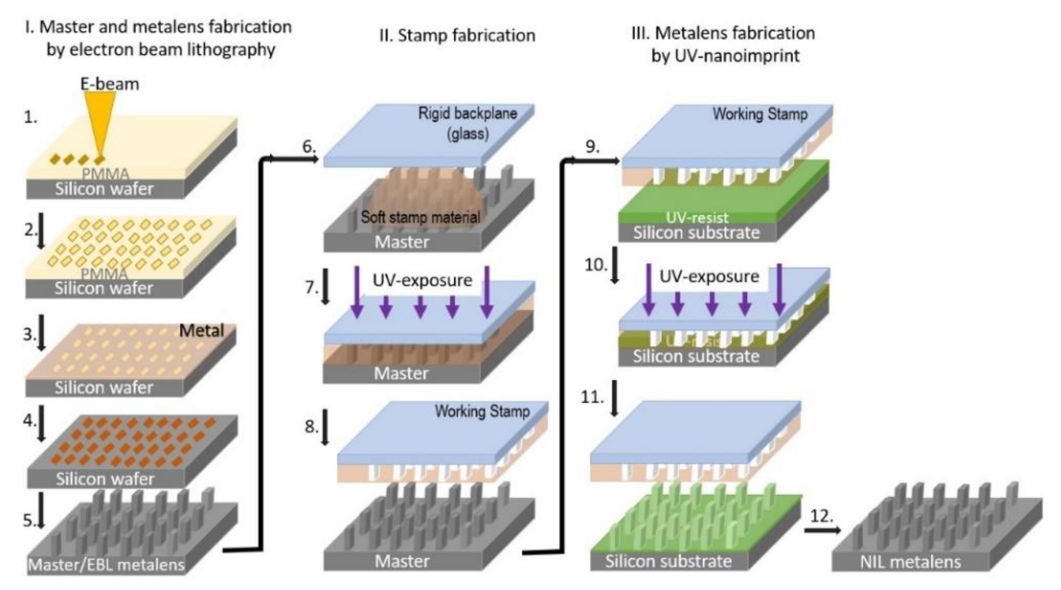
2.2.1. UV-NIL Master and “EBL Metalens” Fabrication
2.2.2. UV-NIL Stamp Fabrication—Master Replication Using UV-PDMS (KER-4690)
2.2.3. UV-NIL Metalenses Fabrication
2.2.4. Optical Measurements of the Metalenses
3. Results and Discussion
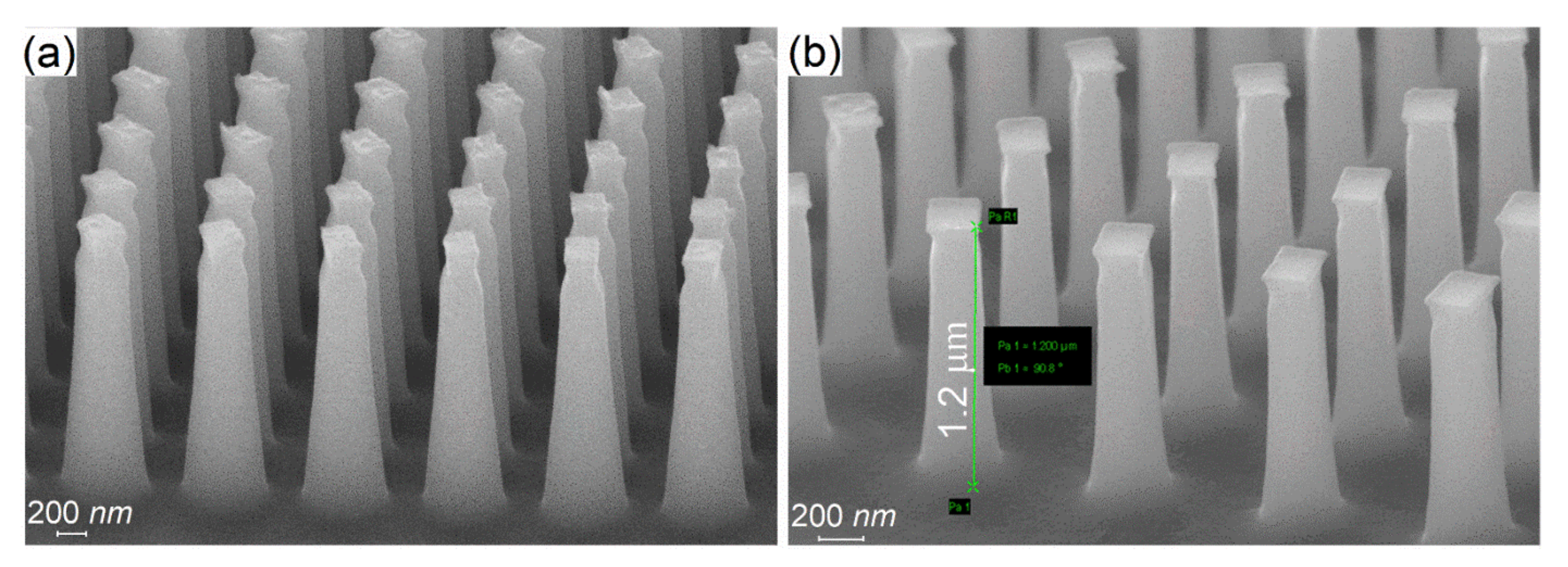
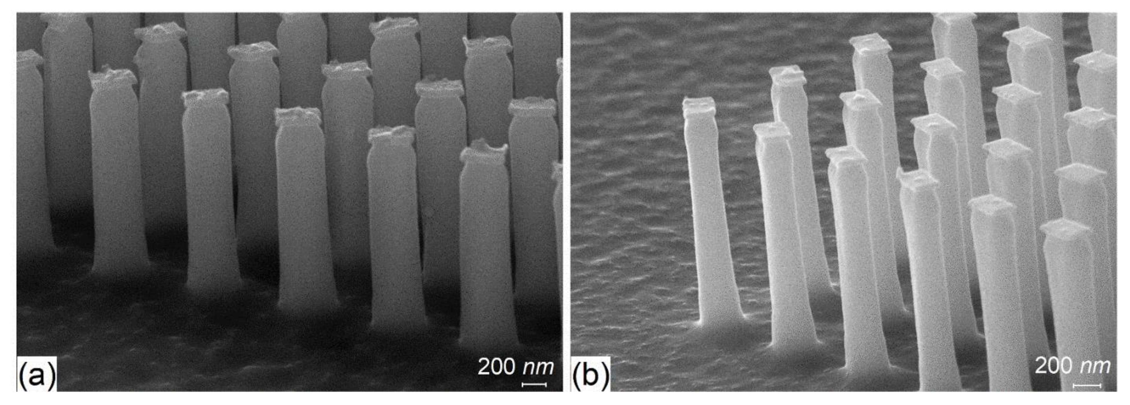
3.1. Master and “EBL Metalens”
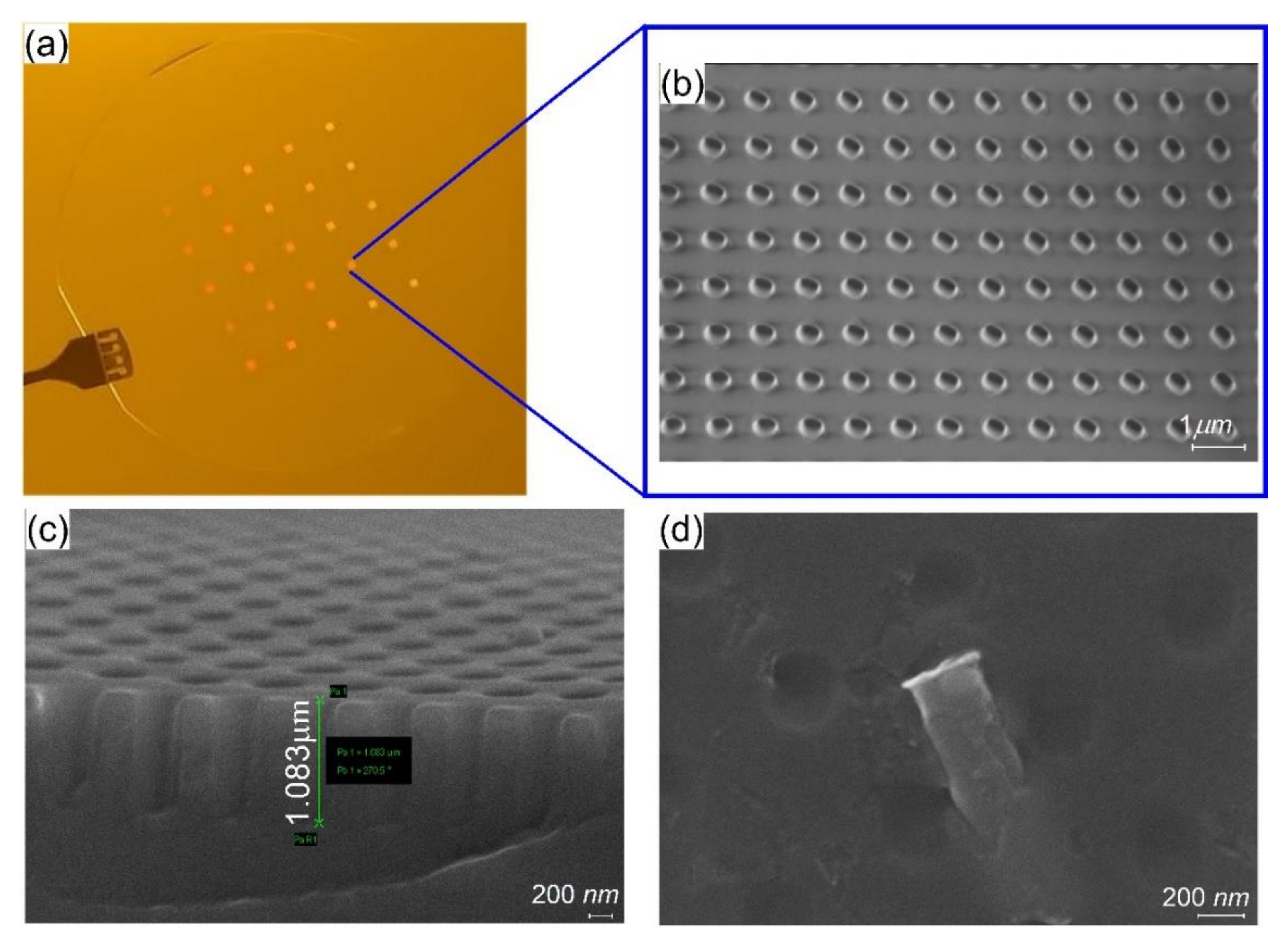
3.2. UV-PDMS Stamp
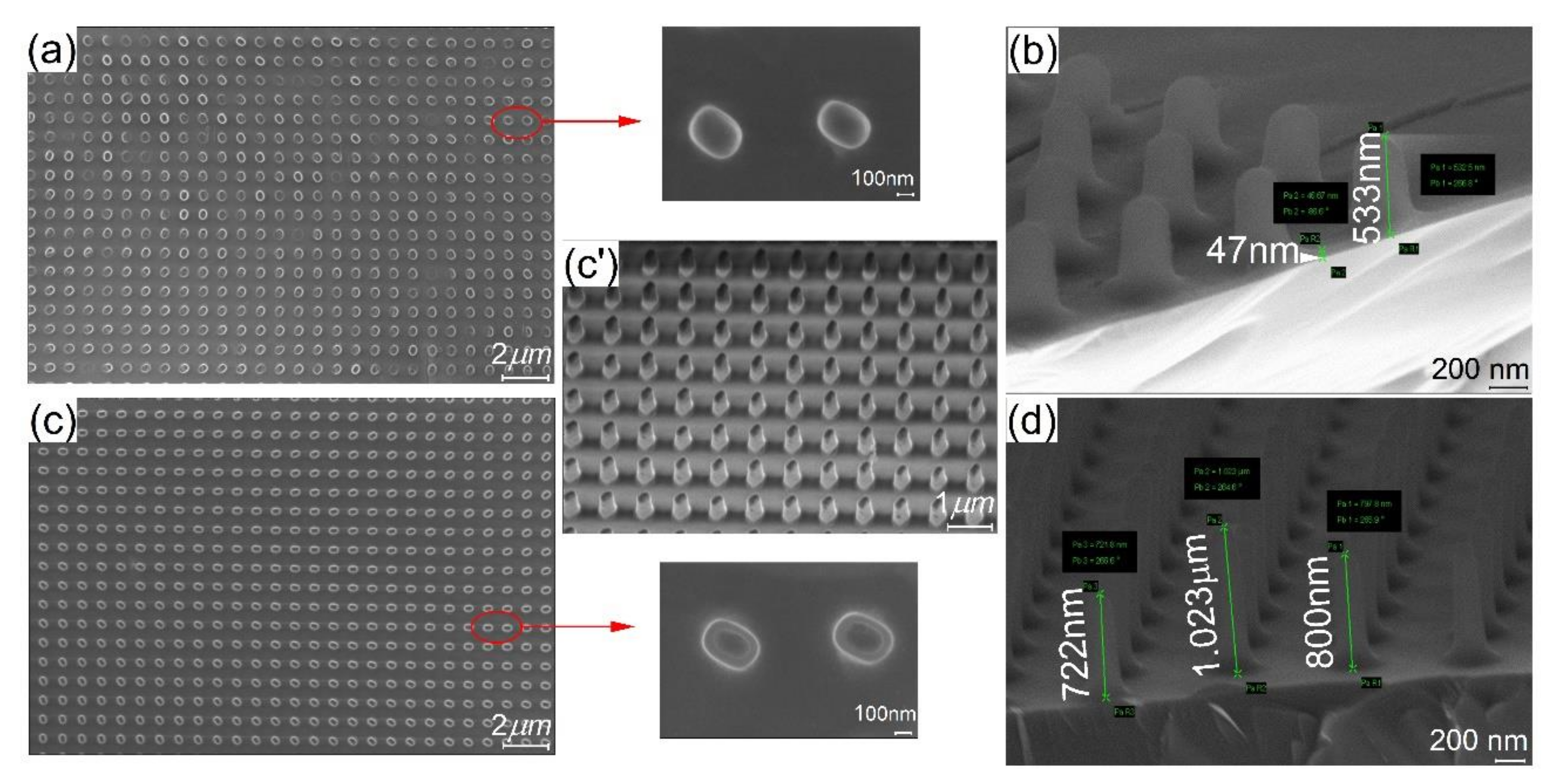
3.3. UV-NIL Metalenses
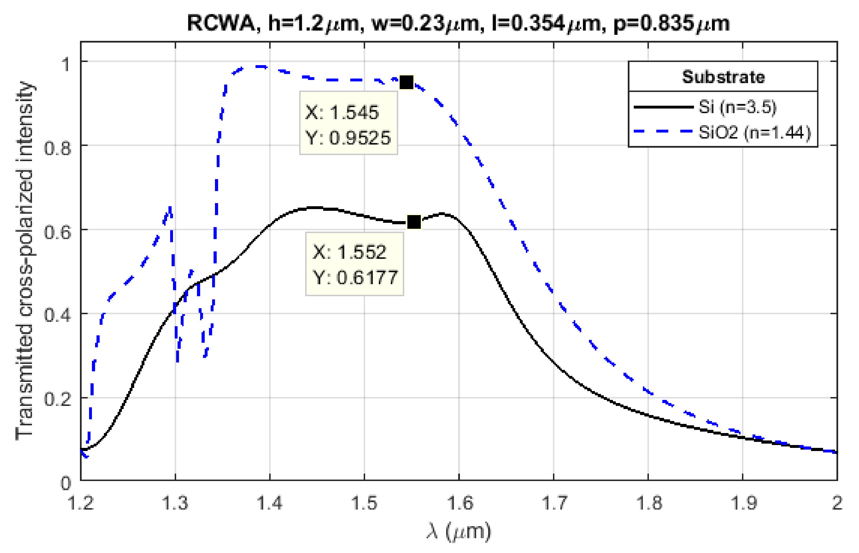
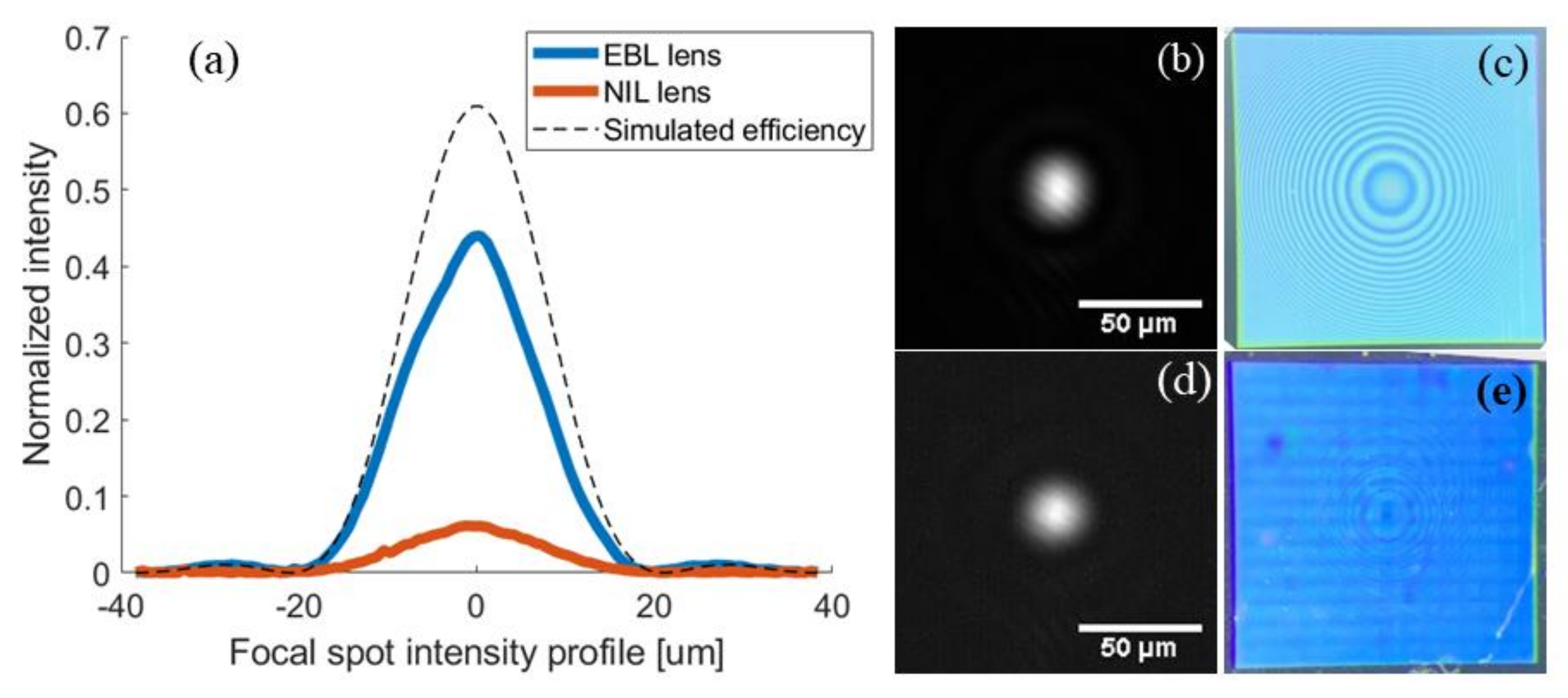
3.4. Optical Measurements of the Metalenses and Supplementary Discussions
4. Conclusions
Author Contributions
Funding
Institutional Review Board Statement
Informed Consent Statement
Data Availability Statement
Acknowledgments
Conflicts of Interest
References
- Kamali, S.M.; Arbabi, E.; Arbabi, A.; Horie, Y.; Faraon, A. Highly tunable elastic dielectric metasurface lenses. Laser Photonics Rev. 2016, 10, 1002–1008. [Google Scholar] [CrossRef] [Green Version]
- Lee, Y.; Kim, S.J.; Park, H.; Lee, B. Metamaterials and metasurfaces for sensor applications. Sensors 2017, 17, 1726. [Google Scholar] [CrossRef] [PubMed] [Green Version]
- Ahmed, R.; Ozen, M.O.; Karaaslan, M.G.; Prator, C.A.; Thanh, C.; Kumar, S.; Torres, L.; Iyer, N.; Munter, S.; Southern, S.; et al. Tunable Fano-Resonant Metasurfaces on a Disposable Plastic-Template for Multimodal and Multiplex Biosensing. Adv. Mater. 2020, 32, 1–11. [Google Scholar] [CrossRef] [PubMed]
- Dirdal, C.A.; Jensen, G.U.; Angelskår, H.; Vaagen Thrane, P.C.; Gjessing, J.; Ordnung, D.A. Towards high-throughput large-area metalens fabrication using UV-nanoimprint lithography and Bosch deep reactive ion etching. Opt. Express 2020, 28, 15542. [Google Scholar] [CrossRef] [PubMed]
- Su, V.-C.; Chu, C.H.; Sun, G.; Tsai, D.P. Advances in optical metasurfaces: Fabrication and applications [Invited]. Opt. Express 2018, 26, 13148. [Google Scholar] [CrossRef]
- La Spada, L. Metasurfaces for advanced sensing and diagnostics. Sensors 2019, 19, 355. [Google Scholar] [CrossRef] [Green Version]
- Khorasaninejad, M.; Capasso, F. Metalenses: Versatile multifunctional photonic components. Science 2017, 358, 8. [Google Scholar] [CrossRef] [PubMed] [Green Version]
- Li, N.; Ho, C.P.; Wang, I.T.; Pitchappa, P.; Fu, Y.H.; Zhu, Y.; Lee, L.Y.T. Spectral imaging and spectral LIDAR systems: Moving toward compact nanophotonics-based sensing. Nanophotonics 2021, 10. [Google Scholar] [CrossRef]
- Arbabi, E.; Arbabi, A.; Kamali, S.M.; Horie, Y.; Faraon, A. Multiwavelength polarization-insensitive lenses based on dielectric metasurfaces with meta-molecules. Optica 2016, 3, 628. [Google Scholar] [CrossRef]
- Gonidec, M.; Hamedi, M.M.; Nemiroski, A.; Rubio, L.M.; Torres, C.; Whitesides, G.M. Fabrication of Nonperiodic Metasurfaces by Microlens Projection Lithography. Nano Lett. 2016, 16, 4125–4132. [Google Scholar] [CrossRef] [PubMed]
- Brière, G.; Ni, P.; Héron, S.; Chenot, S.; Vézian, S.; Brändli, V.; Damilano, B.; Duboz, J.Y.; Iwanaga, M.; Genevet, P. An Etching-Free Approach Toward Large-Scale Light-Emitting Metasurfaces. Adv. Opt. Mater. 2019, 7. [Google Scholar] [CrossRef]
- Paterova, A.V.; Kalashnikov, D.A.; Khaidarov, E.; Yang, H.; Mass, T.W.W.; Paniagua-Domínguez, R.; Kuznetsov, A.I.; Krivitsky, L.A. Non-linear interferometry with infrared metasurfaces. Nanophotonics 2021, 10, 1775–1784. [Google Scholar] [CrossRef]
- Balli, F.; Sultan, M.A.; Ozdemir, A.; Hastings, J.T. An ultrabroadband 3D achromatic metalens. Nanophotonics 2021, 10, 1259–1264. [Google Scholar] [CrossRef]
- Wang, S.; Wu, P.C.; Su, V.C.; Lai, Y.C.; Hung Chu, C.; Chen, J.W.; Lu, S.H.; Chen, J.; Xu, B.; Kuan, C.H.; et al. Broadband achromatic optical metasurface devices. Nat. Commun. 2017, 8, 1–9. [Google Scholar] [CrossRef]
- Kanwal, S.; Wen, J.; Yu, B.; Chen, X.; Kumar, D.; Kang, Y.; Bai, C.; Ubaid, S.; Zhang, D. Polarization insensitive, broadband, near diffraction-limited metalens in ultraviolet region. Nanomaterials 2020, 10, 1439. [Google Scholar] [CrossRef] [PubMed]
- Dragoman, D.; Iftimie, S.; Radu, A. Phase-controlling infrared thermal emitting metasurfaces. J. Opt. 2021, 23, 035103. [Google Scholar] [CrossRef]
- Wang, A.; Chen, Z.; Dan, Y. Planar metalenses in the mid-infrared. AIP Adv. 2019, 9, 1–7. [Google Scholar] [CrossRef] [Green Version]
- Rangelow, I.W. Dry etching-based silicon micro-machining for MEMS. Vacuum 2001, 62, 279–291. [Google Scholar] [CrossRef]
- Guo, H.; Yue, S.; Wang, R.; Hou, Y.; Li, M.; Zhang, K.; Zhang, Z. Design of Polarization-Independent Reflective Metalens in the Ultraviolet–Visible Wavelength Region. Nanomaterials 2021, 11, 1243. [Google Scholar] [CrossRef]
- Bergmair, I.; Dastmalchi, B.; Bergmair, M.; Saeed, A.; Hilber, W.; Hesser, G.; Helgert, C.; Pshenay-Severin, E.; Pertsch, T.; Kley, E.B.; et al. Single and multilayer metamaterials fabricated by nanoimprint lithography. Nanotechnology 2011, 22. [Google Scholar] [CrossRef]
- Khorasaninejad, M.; Chen, W.T.; Devlin, R.C.; Oh, J.; Zhu, A.Y.; Capasso, F. Metalenses at visible wavelengths: Diffraction-limited focusing and subwavelength resolution imaging. Science 2016, 352, 1190–1194. [Google Scholar] [CrossRef] [PubMed] [Green Version]
- Voicu, R.C.; Gavrila, R.; Obreja, A.C.; Baracu, A.M.; Dinescu, A.; Müller, R. Design, microfabrication and analysis of polysilicon thin layers for MEMS vibrating structures. Analog Integr. Circuits Signal. Process. 2015, 82, 611–620. [Google Scholar] [CrossRef]
- Pustan, M.; Chiorean, R.; Birleanu, C.; Dudescu, C.; Muller, R.; Baracu, A.; Voicu, R. Reliability design of thermally actuated MEMS switches based on V-shape beams. Microsyst. Technol. 2017, 23, 3863–3871. [Google Scholar] [CrossRef]
- Li, C.; Yu, P.; Huang, Y.; Zhou, Q.; Wu, J.; Li, Z.; Tong, X.; Wen, Q.; Kuo, H.C.; Wang, Z.M. Dielectric metasurfaces: From wavefront shaping to quantum platforms. Prog. Surf. Sci. 2020, 95, 100584. [Google Scholar] [CrossRef]
- Kasani, S.; Curtin, K.; Wu, N. A review of 2D and 3D plasmonic nanostructure array patterns: Fabrication, light management and sensing applications. Nanophotonics 2019, 8, 2065–2089. [Google Scholar] [CrossRef]
- Hongbo, L.; Ding., L. Nanoimprint Lithography; IntechOpen: London, UK, 2010; Chapter 23; ISBN 978-953-307-064-3. [Google Scholar] [CrossRef] [Green Version]
- Shalaginov, M.Y.; An, S.; Zhang, Y.; Yang, F.; Su, P.; Liberman, V.; Chou, J.B.; Roberts, C.M.; Kang, M.; Rios, C.; et al. Reconfigurable all-dielectric metalens with diffraction-limited performance. arXiv 2019, arXiv:1911.12970. [Google Scholar] [CrossRef]
- Yoon, G.; Kim, K.; Huh, D.; Lee, H.; Rho, J. Single-step manufacturing of hierarchical dielectric metalens in the visible. Nat. Commun. 2020, 11, 2268. [Google Scholar] [CrossRef] [PubMed]
- Yoon, G.; Kim, I.; Rho, J. Challenges in fabrication towards realization of practical metamaterials. Microelectron. Eng. 2016, 163, 7–20. [Google Scholar] [CrossRef]
- Heyderman, L.J.; Schift, H.; David, C.; Ketterer, B.; Auf der Maur, M.; Gobrecht, J. Nanofabrication using hot embossing lithography and electroforming. Microelectron. Eng. 2001, 57–58, 375–380. [Google Scholar] [CrossRef]
- Bhingardive, V.; Menahem, L.; Schvartzman, M. Soft thermal nanoimprint lithography using a nanocomposite mold. Nano Res. 2018, 11, 2705–2714. [Google Scholar] [CrossRef]
- Lim, H.; Jung, S.; Ahn, J.; Choi, K.B.; Kim, G.; Kwon, S.; Lee, J. System for fabrication of large-area roll molds by step-and-repeat liquid transfer imprint lithography. Materials 2020, 13, 1938. [Google Scholar] [CrossRef] [Green Version]
- Dickson, M.N.; Tsao, J.; Liang, E.I.; Navarro, N.I.; Patel, Y.R.; Yee, A.F. Conformal reversal imprint lithography for polymer nanostructuring over large curved geometries. J. Vac. Sci. Technol. B Nanotechnol. Microelectron. Mater. Process. Meas. Phenom. 2017, 35, 021602. [Google Scholar] [CrossRef]
- Lin, C.H.; Chen, R.; Su, C.C.; Chang, F.Y. Ultrasonics for nanoimprint lithography. In Proceedings of the 2005 5th IEEE Conference on Nanotechnology, Nagoya, Japan, 15 July 2005; Volume 2, pp. 460–463. [Google Scholar] [CrossRef]
- Kooy, N.; Mohamed, K.; Pin, L.T.; Guan, O.S. A review of roll-to-roll nanoimprint lithography. Nanoscale Res. Lett. 2014, 9, 1–13. [Google Scholar] [CrossRef] [PubMed] [Green Version]
- Barbillon, G. Soft UV Nanoimprint Lithography: A Tool to Design Plasmonic Nanobiosensors. In Advances in Unconventional Lithography; IntechOpen: London, UK, 2011. [Google Scholar] [CrossRef] [Green Version]
- Lan, H.; Liu, H. UV-nanoimprint lithography: Structure, materials and fabrication of flexible molds. J. Nanosci. Nanotechnol. 2013, 13, 3145–3172. [Google Scholar] [CrossRef] [PubMed]
- Yao, Y.; Liu, H.; Wang, Y.; Li, Y.; Song, B.; Wang, R.P.; Povinelli, M.L.; Wu, W. Nanoimprint-defined, large-area meta-surfaces for unidirectional optical transmission with superior extinction in the visible-to-infrared range. Opt. Express 2016, 24, 15362. [Google Scholar] [CrossRef] [PubMed]
- Tu, P.C.; Lee, Y.C. Droplet spreading nanoimprinting method for micro-/nano-fabrication. J. Micromech. Microeng. 2020, 30. [Google Scholar] [CrossRef]
- Socol, M.; Preda, N.; Rasoga, O.; Costas, A.; Stanculescu, A.; Breazu, C.; Gherendi, F.; Socol, G. Pulsed laser deposition of indium tin oxide thin films on nanopatterned glass substrates. Coatings 2019, 9, 19. [Google Scholar] [CrossRef] [Green Version]
- Stanculescu, A.; Breazu, C.; Socol, M.; Rasoga, O.; Preda, N.; Petre, G.; Solonaru, A.M.; Grigoras, M.; Stanculescu, F.; Socol, G.; et al. Effect of ITO electrode patterning on the properties of organic heterostructures based on non-fullerene acceptor prepared by MAPLE. Appl. Surf. Sci. 2020, 509, 145351. [Google Scholar] [CrossRef]
- Si, S.; Dittrich, L.; Hoffmann, M. Low-cost fabrication of nanoimprint templates with tunable feature sizes at a constant pitch. Microelectron. Eng. 2017, 170, 34–38. [Google Scholar] [CrossRef]
- Li, M.; Chen, Y.; Luo, W.; Cheng, X. Interfacial interactions during demolding in nanoimprint lithography. Micromachines 2021, 12, 349. [Google Scholar] [CrossRef]
- Tochino, T.; Shiotsu, T.; Uemura, K.; Yasuda, M.; Kawata, H.; Hirai, Y. Impact of resist shrinkage on the template release process in nanoimprint lithography. J. Vac. Sci. Technol. B Nanotechnol. Microelectron. Mater. Process. Meas. Phenom. 2014, 32, 06FG08. [Google Scholar] [CrossRef]
- Zhu, Z.; Li, Q.; Zhang, L.; Chen, M.; Fan, S. UV-based nanoimprinting lithography with a fluorinated flexible stamp. J. Vac. Sci. Technol. B Nanotechnol. Microelectron. Mater. Process. Meas. Phenom. 2011, 29, 021015. [Google Scholar] [CrossRef]
- Traub, M.C.; Longsine, W.; Truskett, V.N. Advances in Nanoimprint Lithography. Annu. Rev. Chem. Biomol. Eng. 2016, 7, 583–604. [Google Scholar] [CrossRef] [PubMed]
- Baracu, A.M.; Dirdal, C.A.; Avram, A.M.; Dinescu, A.; Muller, R.; Jensen, G.U.; Thrane, P.C.V.; Angelskår, H. Metasurface Fabrication by Cryogenic and Bosch Deep Reactive Ion Etching. Micromachines 2021, 21, 13. [Google Scholar]
- Li, B.; Piyawattanametha, W.; Qiu, Z. Metalens-based miniaturized optical systems. Micromachines 2019, 10, 310. [Google Scholar] [CrossRef] [Green Version]
- Yu, N.; Capasso, F. Flat optics with designer metasurfaces. Nat. Mater. 2014, 13, 139–150. [Google Scholar] [CrossRef]
- Chen, W.T.; Zhu, A.Y.; Sisler, J.; Bharwani, Z.; Capasso, F. A broadband achromatic polarization-insensitive metalens consisting of anisotropic nanostructures. Nat. Commun. 2019, 10, 1–7. [Google Scholar] [CrossRef] [PubMed] [Green Version]
- Kang, M.; Feng, T.; Wang, H.-T.; Li, J. Wave front engineering from an array of thin aperture antennas. Opt. Express 2012, 20, 15882. [Google Scholar] [CrossRef] [PubMed]
- Arbabi, A.; Arbabi, E.; Mansouree, M.; Han, S.; Kamali, S.M.; Horie, Y.; Faraon, A. Increasing efficiency of high numerical aperture metasurfaces using the grating averaging technique. Sci. Rep. 2020, 10, 1–10. [Google Scholar] [CrossRef]
- Wolf, J.; Gruetzner, S.; Ferstl, M.; Klein, J.J.; Schleunitz, A.; Gruetzner, G. Prototyping of Monolithic Diffractive-Refractive Micro-Optics with Inkjetable Polymers. In Optical Design and Fabrication 2019 (Freeform, OFT); OSA Technical Digest, Paper OT2A.5; Optical Society of America: Washington, DC, USA, 2019. [Google Scholar]
- Messerschmidt, M.; Greer, A.; Schlachter, F.; Barnett, J.; Thesen, M.W.; Gadegaard, N.; Grützner, G.; Schleunitz, A. New organic photo-curable nanoimprint resist «mr-NIL210» for high volume fabrication applying soft PDMS-based stamps. J. Photopolym. Sci. Technol. 2017, 30, 605–611. [Google Scholar] [CrossRef] [Green Version]


| ICP Power | RF Power | Pressure | SF6 Flow | O2 Flow | Table Temperature |
|---|---|---|---|---|---|
| 1200 W | 3 W | 7.5 mTorr | 60 sccm | 8 sccm | −115 °C |
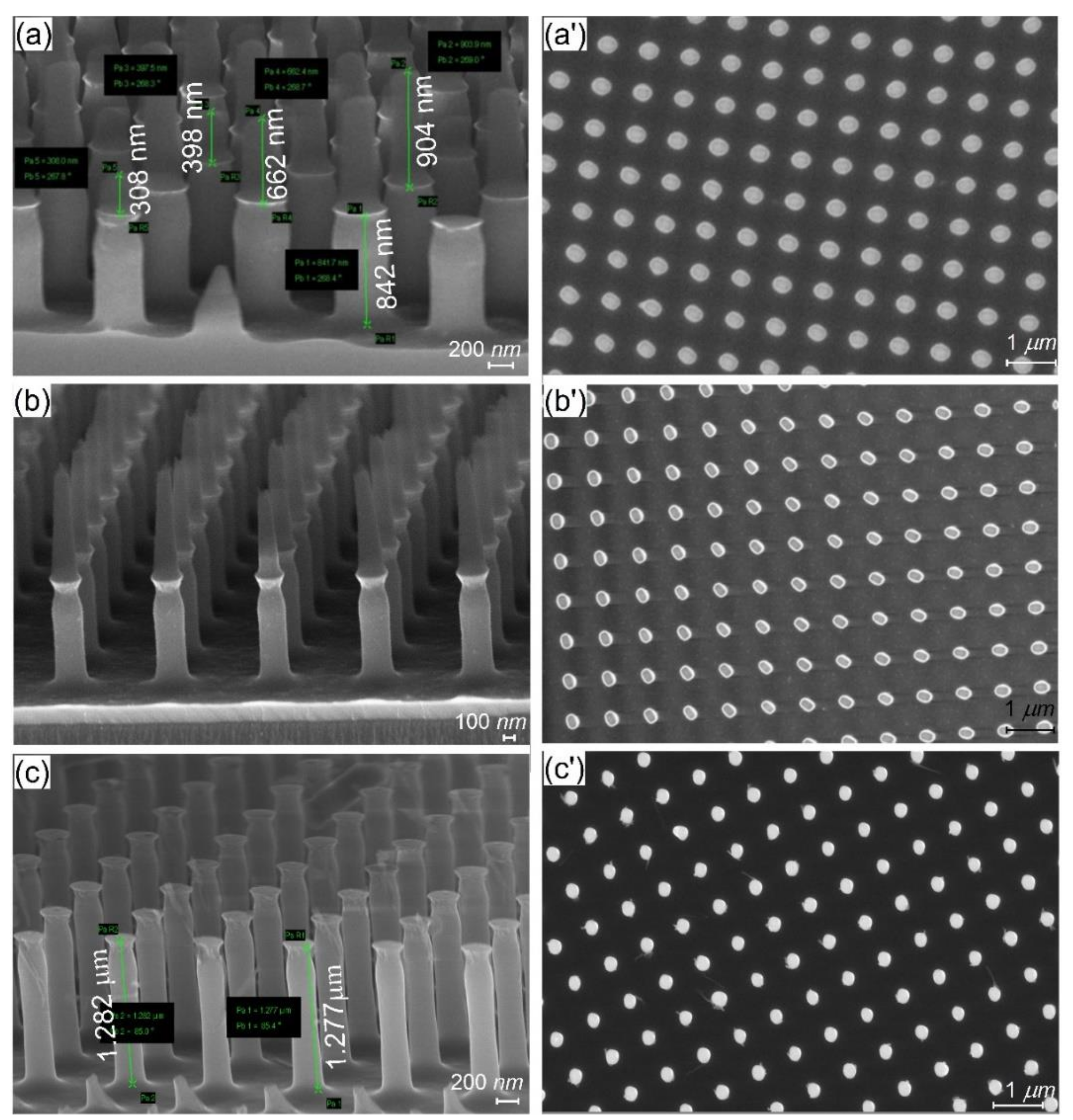
| Sample | Dimensions | Deviation From Target | ||||
|---|---|---|---|---|---|---|
| Height-h (µm) | Width-w (nm) | Length-l (nm) | Height (%) | Width (%) | Length (%) | |
| Target | 1200 | 230 | 354 | - | - | - |
| EBL metalens | 1200 | 236.8 | 355.2 | 0 | −2.96 | −0.33 |
| Stamp 1 | 1083 | 224.2 | 340.4 | 9.75 | 2.52 | 3.84 |
| UV-NIL metalens 1 | 842 | 235.9 | 312.6 | 29.83 | −2.57 | 11.19 |
| UV-NIL metalens 2 | 1066 | 210.3 | 302.6 | 11.16 | 8.56 | 14.52 |
| UV-NIL metalens 3 | 1280 | 247.2 | 307 | −6.66 | −7.48 | 13.27 |
Publisher’s Note: MDPI stays neutral with regard to jurisdictional claims in published maps and institutional affiliations. |
© 2021 by the authors. Licensee MDPI, Basel, Switzerland. This article is an open access article distributed under the terms and conditions of the Creative Commons Attribution (CC BY) license (https://creativecommons.org/licenses/by/4.0/).
Share and Cite
Baracu, A.M.; Avram, M.A.; Breazu, C.; Bunea, M.-C.; Socol, M.; Stanculescu, A.; Matei, E.; Thrane, P.C.V.; Dirdal, C.A.; Dinescu, A.; et al. Silicon Metalens Fabrication from Electron Beam to UV-Nanoimprint Lithography. Nanomaterials 2021, 11, 2329. https://doi.org/10.3390/nano11092329
Baracu AM, Avram MA, Breazu C, Bunea M-C, Socol M, Stanculescu A, Matei E, Thrane PCV, Dirdal CA, Dinescu A, et al. Silicon Metalens Fabrication from Electron Beam to UV-Nanoimprint Lithography. Nanomaterials. 2021; 11(9):2329. https://doi.org/10.3390/nano11092329
Chicago/Turabian StyleBaracu, Angela Mihaela, Marius Andrei Avram, Carmen Breazu, Mihaela-Cristina Bunea, Marcela Socol, Anca Stanculescu, Elena Matei, Paul Conrad Vaagen Thrane, Christopher Andrew Dirdal, Adrian Dinescu, and et al. 2021. "Silicon Metalens Fabrication from Electron Beam to UV-Nanoimprint Lithography" Nanomaterials 11, no. 9: 2329. https://doi.org/10.3390/nano11092329
APA StyleBaracu, A. M., Avram, M. A., Breazu, C., Bunea, M.-C., Socol, M., Stanculescu, A., Matei, E., Thrane, P. C. V., Dirdal, C. A., Dinescu, A., & Rasoga, O. (2021). Silicon Metalens Fabrication from Electron Beam to UV-Nanoimprint Lithography. Nanomaterials, 11(9), 2329. https://doi.org/10.3390/nano11092329