
Effect of Nitrogen Doping on the Crystallization Kinetics of Ge2Sb2Te5

 ,
,  ,
,
Abstract
:1. Introduction
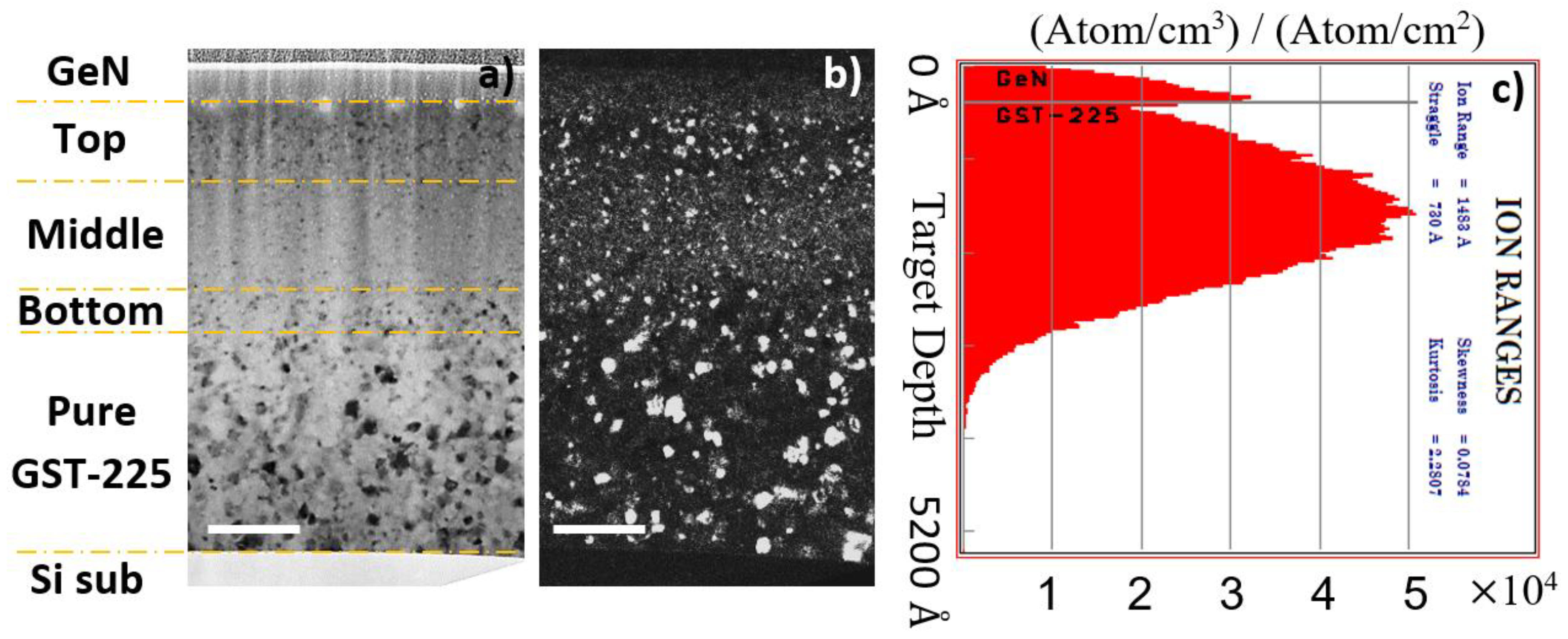
2. Experimental
3. Results and Discussion
3.1. Crystallization Kinetics
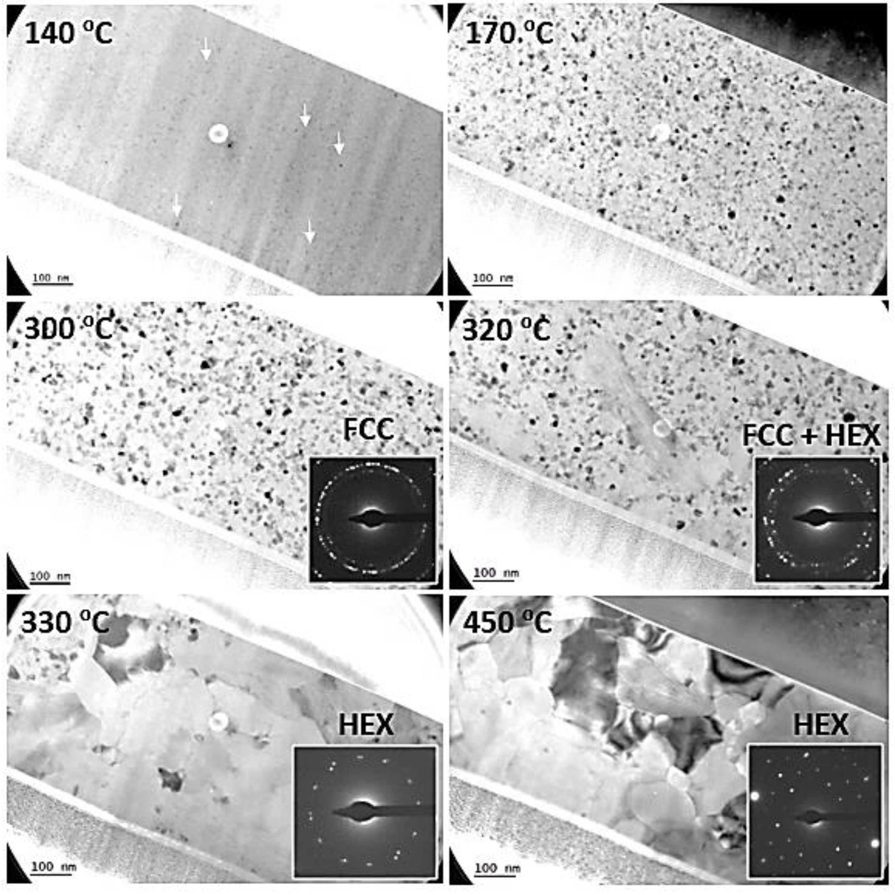
3.1.1. Pristine Sample
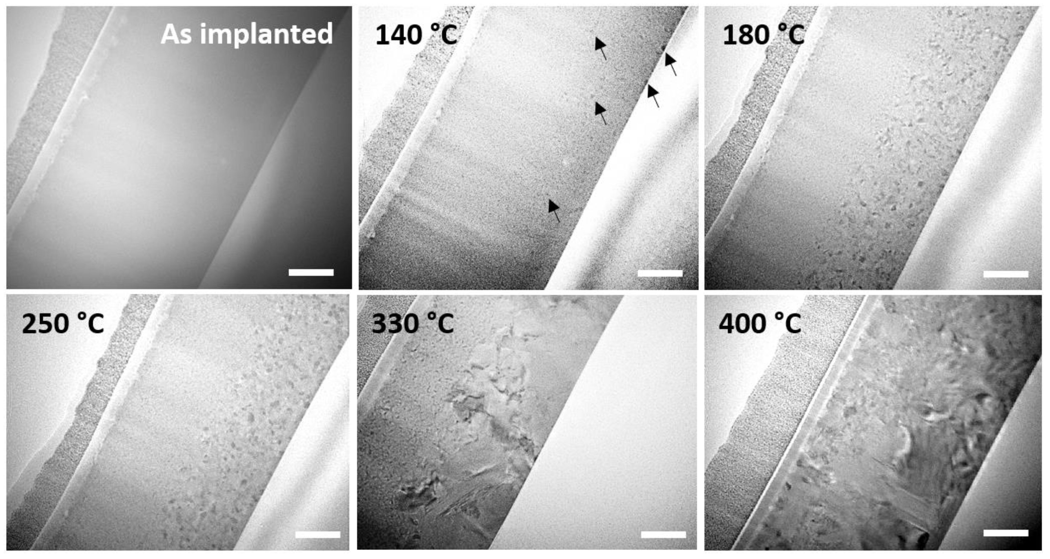
3.1.2. N-Implanted Samples
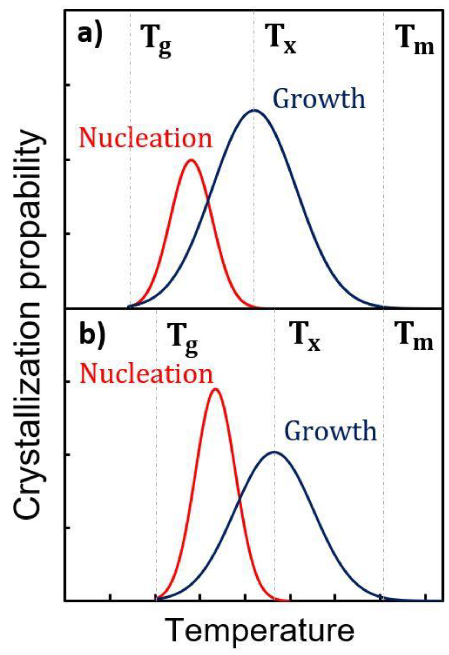
4. Discussion
Strain in the Grains: N Location
5. Conclusions
Supplementary Materials
Author Contributions
Funding
Data Availability Statement
Conflicts of Interest
References
- Wuttig, M.; Yamada, N. Phase-Change Materials for Rewriteable Data Storage. Nat. Mater. 2007, 6, 824–832. [Google Scholar] [CrossRef] [PubMed]
- Lee, B.C.; Zhou, P.; Yang, J.; Zhang, Y.; Zhao, B.; Ipek, E.; Mutlu, O.; Burger, D. Phase-Change Technology and the Future of Main Memory. IEEE Micro 2010, 30, 143. [Google Scholar] [CrossRef]
- Raoux, S.; Wełnic, W.; Ielmini, D. Phase Change Materials and Their Application to Nonvolatile Memories. Chem. Rev. 2010, 110, 240–267. [Google Scholar] [CrossRef] [PubMed]
- Noé, P.; Vallée, C.; Hippert, F.; Fillot, F.; Raty, J.-Y. Phase-Change Materials for Non-Volatile Memory Devices: From Technological Challenges to Materials Science Issues. Semicond. Sci. Technol. 2018, 33, 013002. [Google Scholar] [CrossRef]
- Guo, P.; Sarangan, A.; Agha, I. A Review of Germanium-Antimony-Telluride Phase Change Materials for Non-Volatile Memories and Optical Modulators. Appl. Sci. 2019, 9, 530. [Google Scholar] [CrossRef] [Green Version]
- Bruns, G.; Merkelbach, P.; Schlockermann, C.; Salinga, M.; Wuttig, M.; Happ, T.D.; Philipp, J.B.; Kund, M. Nanosecond Switching in GeTe Phase Change Memory Cells. Appl. Phys. Lett. 2009, 95, 043108. [Google Scholar] [CrossRef]
- Loke, D.; Lee, T.H.; Wang, W.J.; Shi, L.P.; Zhao, R.; Yeo, Y.C.; Chong, T.C.; Elliott, S.R. Breaking the Speed Limits of Phase-Change Memory. Science 2012, 336, 1566–1569. [Google Scholar] [CrossRef] [Green Version]
- Ielmini, D.; Wong, H.-S.P. In-Memory Computing with Resistive Switching Devices. Nat. Electron. 2018, 1, 333–343. [Google Scholar] [CrossRef]
- Islam, R.; Li, H.; Chen, P.-Y.; Wan, W.; Chen, H.-Y.; Gao, B.; Wu, H.; Yu, S.; Saraswat, K.; Philip Wong, H.-S. Device and Materials Requirements for Neuromorphic Computing. J. Phys. Appl. Phys. 2019, 52, 113001. [Google Scholar] [CrossRef]
- Spiga, S.; Sebastian, A.; Querlioz, D.; Rajendran, B. Memristive Devices for Brain-Inspired Computing, 1st ed.; Woodhead Publishing Series in Electronic and Optical Materials Series. Available online: https://www.elsevier.com/books/memristive-devices-for-brain-inspired-computing/spiga/978-0-08-102782-0 (accessed on 24 May 2021).
- Redaelli, A. Self-Consistent Numerical Model. In Phase Change Memory; Redaelli, A., Ed.; Springer International Publishing: Cham, Switzerland, 2018; pp. 65–88. [Google Scholar] [CrossRef]
- Zhou, X.; Xia, M.; Rao, F.; Wu, L.; Li, X.; Song, Z.; Feng, S.; Sun, H. Understanding Phase-Change Behaviors of Carbon-Doped Ge2Sb2Te5 for Phase-Change Memory Application. ACS Appl. Mater. Interfaces 2014, 6, 14207–14214. [Google Scholar] [CrossRef]
- Jeong, T.H.; Seo, H.; Lee, K.L.; Choi, S.M.; Kim, S.J.; Kim, S.Y. Study of Oxygen-Doped GeSbTe Film and Its Effect as an Interface Layer on the Recording Properties in the Blue Wavelength. Jpn. J. Appl. Phys. 2001, 40, 1609–1612. [Google Scholar] [CrossRef]
- Wang, K.; Wamwangi, D.; Ziegler, S.; Steimer, C.; Wuttig, M. Influence of Bi Doping upon the Phase Change Characteristics of Ge2Sb2Te5. J. Appl. Phys. 2004, 96, 5557–5562. [Google Scholar] [CrossRef]
- Choi, K.-J.; Yoon, S.-M.; Lee, N.-Y.; Lee, S.-Y.; Park, Y.-S.; Yu, B.-G.; Ryu, S.-O. The Effect of Antimony-Doping on Ge2Sb2Te5, a Phase Change Material. Thin Solid Films 2008, 516, 8810–8812. [Google Scholar] [CrossRef]
- Kim, K.-H.; Chung, J.-G.; Kyoung, Y.K.; Park, J.-C.; Choi, S.-J. Phase-Change Characteristics of Nitrogen-Doped Ge2Sb2Te5 Films during Annealing Process. J. Mater. Sci. Mater. Electron. 2011, 22, 52–55. [Google Scholar] [CrossRef]
- Navarro, G.; Sousa, V.; Noe, P.; Castellani, N.; Coue, M.; Kluge, J.; Kiouseloglou, A.; Sabbione, C.; Persico, A.; Roule, A.; et al. N-Doping Impact in Optimized Ge-Rich Materials Based Phase-Change Memory. In Proceedings of the 2016 IEEE 8th International Memory Workshop (IMW), Paris, France, 15–18 May 2016; pp. 1–4. [Google Scholar] [CrossRef]
- Luong, M.A.; Wen, D.; Rahier, E.; Ratel Ramond, N.; Pecassou, B.; Le Friec, Y.; Benoit, D.; Claverie, A. Impact of Nitrogen on the Crystallization and Microstructure of Ge-Rich GeSbTe Alloys. Phys. Status Solidi RRL Rapid Res. Lett. 2021, 15, 2000443. [Google Scholar] [CrossRef]
- Luong, M.A.; Agati, M.; Ratel Ramond, N.; Grisolia, J.; Le Friec, Y.; Benoit, D.; Claverie, A. On Some Unique Specificities of Ge-Rich GeSbTe Phase-Change Material Alloys for Nonvolatile Embedded-Memory Applications. Phys. Status Solidi Rapid Res. Lett. 2021, 15, 2000471. [Google Scholar] [CrossRef]
- Shelby, R.M.; Raoux, S. Crystallization Dynamics of Nitrogen-Doped Ge2Sb2Te5. J. Appl. Phys. 2009, 105, 104902. [Google Scholar] [CrossRef]
- Yu, X.; Zhao, Y.; Li, C.; Hu, C.; Ma, L.; Fan, S.; Zhao, Y.; Min, N.; Tao, S.; Wang, Y. Improved Multi-Level Data Storage Properties of Germanium-Antimony-Tellurium Films by Nitrogen Doping. Scr. Mater. 2017, 141, 120–124. [Google Scholar] [CrossRef]
- Kim, Y.; Baeck, J.H.; Cho, M.-H.; Jeong, E.J.; Ko, D.-H. Effects of N2+ Ion Implantation on Phase Transition in Ge2Sb2Te5 Films. J. Appl. Phys. 2006, 100, 083502. [Google Scholar] [CrossRef]
- Privitera, S.; Rimini, E.; Zonca, R. Amorphous-to-Crystal Transition of Nitrogen- and Oxygen-Doped Ge2Sb2Te5 Films Studied by In Situ Resistance Measurements. Appl. Phys. Lett. 2004, 85, 3044–3046. [Google Scholar] [CrossRef]
- Lai, Y.; Qiao, B.; Feng, J.; Ling, Y.; Lai, L.; Lin, Y.; Tang, T.; Cai, B.; Chen, B. Nitrogen-Doped Ge2Sb2Te5 Films for Nonvolatile Memory. J. Electron. Mater. 2005, 34, 176–181. [Google Scholar] [CrossRef]
- Wimmer, M.; Kaes, M.; Dellen, C.; Salinga, M. Role of Activation Energy in Resistance Drift of Amorphous Phase Change Materials. Front. Phys. 2014, 2. [Google Scholar] [CrossRef] [Green Version]
- Noé, P.; Sabbione, C.; Castellani, N.; Veux, G.; Navarro, G.; Sousa, V.; Hippert, F.; d’Acapito, F. Structural Change with the Resistance Drift Phenomenon in Amorphous GeTe Phase Change Materials’ Thin Films. J. Phys. Appl. Phys. 2016, 49, 035305. [Google Scholar] [CrossRef] [Green Version]
- Park, I.-M.; Cho, J.-Y.; Yang, T.-Y.; Park, E.S.; Joo, Y.-C. Thermomechanical Analysis on the Phase Stability of Nitrogen-Doped Amorphous Ge2Sb2Te5 Films. Jpn. J. Appl. Phys. 2011, 50, 061201. [Google Scholar] [CrossRef]
- Jeong, T.H.; Kim, M.R.; Seo, H.; Park, J.W.; Yeon, C. Crystal Structure and Microstructure of Nitrogen-Doped Ge2Sb2Te5 Thin Film. Jpn. J. Appl. Phys. 2000, 39, 2775–2779. [Google Scholar] [CrossRef]
- Kooi, B.J.; Groot, W.M.G.; De Hosson, J.T.M. In Situ Transmission Electron Microscopy Study of the Crystallization of Ge2Sb2Te5. J. Appl. Phys. 2004, 95, 924–932. [Google Scholar] [CrossRef] [Green Version]
- Liu, B.; Song, Z.; Zhang, T.; Xia, J.; Feng, S.; Chen, B. Effect of N-Implantation on the Structural and Electrical Characteristics of Ge2Sb2Te5 Phase Change Film. Thin Solid Films 2005, 478, 49–55. [Google Scholar] [CrossRef]
- Kim, K.-H.; Park, J.-C.; Lee, J.-H.; Chung, J.-G.; Heo, S.; Choi, S.-J. Nitrogen-Doping Effect on Ge2Sb2Te5 Chalcogenide Alloy Films during Annealing. Jpn. J. Appl. Phys. 2010, 49, 101201. [Google Scholar] [CrossRef]
- Kim, Y.; Jeong, K.; Cho, M.-H.; Hwang, U.; Jeong, H.S.; Kim, K. Changes in the Electronic Structures and Optical Band Gap of Ge2Sb2Te5 and N-Doped Ge2Sb2Te5 during Phase Transition. Appl. Phys. Lett. 2007, 90, 171920. [Google Scholar] [CrossRef]
- Caravati, S.; Colleoni, D.; Mazzarello, R.; Kühne, T.D.; Krack, M.; Bernasconi, M.; Parrinello, M. First-Principles Study of Nitrogen Doping in Cubic and Amorphous Ge2Sb2Te5. J. Phys. Condens. Matter 2011, 23, 265801. [Google Scholar] [CrossRef]
- Kojima, R.; Okabayashi, S.; Kashihara, T.; Horai, K.; Matsunaga, T.; Ohno, E.; Yamada, N.; Ohta, T. Nitrogen Doping Effect on Phase Change Optical Disks. Jpn. J. Appl. Phys. 1998, 37, 2098–2103. [Google Scholar] [CrossRef]
- Wang, W.; Loke, D.; Shi, L.; Zhao, R.; Yang, H.; Law, L.-T.; Ng, L.-T.; Lim, K.-G.; Yeo, Y.-C.; Chong, T.-C.; et al. Enabling Universal Memory by Overcoming the Contradictory Speed and Stability Nature of Phase-Change Materials. Sci. Rep. 2012, 2, 360. [Google Scholar] [CrossRef] [Green Version]
- Bert, N.A.; Chaldyshev, V.V.; Cherkashin, N.A.; Nevedomskiy, V.N.; Preobrazhenskii, V.V.; Putyato, M.A.; Semyagin, B.R.; Ushanov, V.I.; Yagovkina, M.A. Metallic AsSb Nanoinclusions Strongly Enriched by Sb in AlGaAsSb Metamaterial. J. Appl. Phys. 2019, 125, 145106. [Google Scholar] [CrossRef]
- 80pm Resolution Reached by the New CEMES-Hitachi I2TEM Microscope. Actualités Next Toulouse, Nano, Mesures Extrêmes, Théorie. Laboratoires Recherche Physique Chimie. Available online: http://www.next-toulouse.eu/news/80pm-resolution-reached-by-the-new-cemes-hitachi-i2tem-microscope-en (accessed on 24 May 2021).
- Agati, M.; Gay, C.; Benoit, D.; Claverie, A. Effects of Surface Oxidation on the Crystallization Characteristics of Ge-Rich Ge-Sb-Te Alloys Thin Films. Appl. Surf. Sci. 2020, 518, 146227. [Google Scholar] [CrossRef]
- James Ziegler—SRIM & TRIM. Available online: http://www.srim.org/ (accessed on 24 May 2021).
- Fantini, A.; Sousa, V.; Perniola, L.; Gourvest, E.; Bastien, J.; Maitrejean, S.; Braga, S.; Pashkov, N.; Bastard, A.; Hyot, B.; et al. N-Doped GeTe as Performance Booster for Embedded Phase-Change Memories. In Proceedings of the 2010 International Electron Devices Meeting, San Francisco, CA, USA, 6–10 December 2010; pp. 29.1.1–29.1.4. [Google Scholar] [CrossRef]
- Burr, G.W.; Breitwisch, M.J.; Franceschini, M.; Garetto, D.; Gopalakrishnan, K.; Jackson, B.; Kurdi, B.; Lam, C.; Lastras, L.A.; Padilla, A.; et al. Phase Change Memory Technology. J. Vac. Sci. Technol. B Nanotechnol. Microelectron. Mater. Process. Meas. Phenom. 2010, 28, 223–262. [Google Scholar] [CrossRef] [Green Version]
- Kalb, J.A. Crystallization Kinetics. In Phase Change Materials; Raoux, S., Wuttig, M., Eds.; Springer: Boston, MA, USA, 2009. [Google Scholar] [CrossRef]
- Redaelli, A. An Introduction on Phase-Change Memories. In Phase Change Memory; Redaelli, A., Ed.; Springer International Publishing: Cham, Switzerland, 2018; pp. 1–10. [Google Scholar] [CrossRef]
- Lee, T.H.; Loke, D.; Elliott, S.R. Microscopic Mechanism of Doping-Induced Kinetically Constrained Crystallization in Phase-Change Materials. Adv. Mater. 2015, 27, 5477–5483. [Google Scholar] [CrossRef]
- Song, S.A.; Zhang, W.; Sik Jeong, H.; Kim, J.-G.; Kim, Y.-J. In Situ Dynamic HR-TEM and EELS Study on Phase Transitions of Ge2Sb2Te5 Chalcogenides. Ultramicroscopy 2008, 108, 1408–1419. [Google Scholar] [CrossRef]
- Hytch, M.J. Analysis of Variations in Structure from High Resolution Electron Microscope Images by Combining Real Space and Fourier Space Information. Microsc. Microanal. Microstruct. 1997, 8, 41–57. [Google Scholar] [CrossRef]
- Bierwolf, R.; Hohenstein, M.; Phillipp, F.; Brandt, O.; Crook, G.E.; Ploog, K. Direct Measurement of Local Lattice Distortions in Strained Layer Structures by HREM. Ultramicroscopy 1993, 49, 273–285. [Google Scholar] [CrossRef]
- Usuda, K.; Numata, T.; Irisawa, T.; Hirashita, N.; Takagi, S. Strain Characterization in SOI and Strained-Si on SGOI MOSFET Channel Using Nano-Beam Electron Diffraction (NBD). Mater. Sci. Eng. B 2005, 124–125, 143–147. [Google Scholar] [CrossRef]
- Hÿtch, M.; Houdellier, F.; Hüe, F.; Snoeck, E. Nanoscale Holographic Interferometry for Strain Measurements in Electronic Devices. Nature 2008, 453, 1086–1089. [Google Scholar] [CrossRef]
- Louiset, A.; Schamm-Chardon, S.; Kononchuk, O.; Cherkashin, N. Reconstruction of Depth Resolved Strain Tensor in Off-Axis Single Crystals: Application to H+ Ions Implanted LiTaO3. Appl. Phys. Lett. 2021, 118, 082903. [Google Scholar] [CrossRef]
- Kim, K.; Park, J.-C.; Chung, J.-G.; Song, S.A.; Jung, M.-C.; Lee, Y.M.; Shin, H.-J.; Kuh, B.; Ha, Y.; Noh, J.-S. Observation of Molecular Nitrogen in N-doped Ge2Sb2Te5. Appl. Phys. Lett. 2006, 89, 243520. [Google Scholar] [CrossRef]


| Temperature (°C) | 140 | 160 | 170 | 180 | 200 | 230 | 270 | 300 |
| Grain Size (±3 nm) | 5 | 10 | 12 | 15 | 18 | 20 | 23 | 30 |
| Top | Middle (Rp Region) | Bottom | Unimplanted | |
|---|---|---|---|---|
| 175 °C—30 min | 0 (few isolated) | 0 (none) | 0 (few isolated) | 18 nm ± 2 nm |
| 180 °C—30 min | 6 nm ± 2 nm | 2 nm ± 2 nm | 6 nm ± 2 nm | 20 nm ± 2 nm |
| 210 °C—30 min | 8 nm ± 2 nm | 6 nm ± 2 nm | 8 nm ± 2 nm | 20 nm ± 2 nm |
| 250 °C—30 min | 10 nm ± 2 nm | 10 nm ± 2 nm | 10 nm ± 2 nm | 22 nm ± 2 nm |
| 300 °C—1 h | 10 nm ± 2 nm | 10 nm ± 2 nm | 10 nm ± 2 nm | >80 nm |
Publisher’s Note: MDPI stays neutral with regard to jurisdictional claims in published maps and institutional affiliations. |
© 2021 by the authors. Licensee MDPI, Basel, Switzerland. This article is an open access article distributed under the terms and conditions of the Creative Commons Attribution (CC BY) license (https://creativecommons.org/licenses/by/4.0/).
Share and Cite
Luong, M.A.; Cherkashin, N.; Pecassou, B.; Sabbione, C.; Mazen, F.; Claverie, A. Effect of Nitrogen Doping on the Crystallization Kinetics of Ge2Sb2Te5. Nanomaterials 2021, 11, 1729. https://doi.org/10.3390/nano11071729
Luong MA, Cherkashin N, Pecassou B, Sabbione C, Mazen F, Claverie A. Effect of Nitrogen Doping on the Crystallization Kinetics of Ge2Sb2Te5. Nanomaterials. 2021; 11(7):1729. https://doi.org/10.3390/nano11071729
Chicago/Turabian StyleLuong, Minh Anh, Nikolay Cherkashin, Béatrice Pecassou, Chiara Sabbione, Frédéric Mazen, and Alain Claverie. 2021. "Effect of Nitrogen Doping on the Crystallization Kinetics of Ge2Sb2Te5" Nanomaterials 11, no. 7: 1729. https://doi.org/10.3390/nano11071729
APA StyleLuong, M. A., Cherkashin, N., Pecassou, B., Sabbione, C., Mazen, F., & Claverie, A. (2021). Effect of Nitrogen Doping on the Crystallization Kinetics of Ge2Sb2Te5. Nanomaterials, 11(7), 1729. https://doi.org/10.3390/nano11071729