Article

Two-Channel VO2 Memory Meta-Device for Terahertz Waves

1
College of Materials Science and Engineering, Sichuan University, Chengdu 610065, China
2
Department of Basic Sciences, Air Force Engineering University, Xi’an 710051, China
3
School of Engineering, The University of Manchester, Manchester M13 9PL, UK
4
Hubei Engineering Research Center of RF-Microwave Technology and Application, School of Science, Wuhan University of Technology, Wuhan 430070, China
5
State Key Laboratory of Millimeter Waves, Department of Radio Engineering, Southeast University, Nanjing 210096, China
*
Authors to whom correspondence should be addressed.
Nanomaterials 2021, 11(12), 3409; https://doi.org/10.3390/nano11123409
Submission received: 12 November 2021 / Revised: 11 December 2021 / Accepted: 12 December 2021 / Published: 16 December 2021
(This article belongs to the Special Issue Advances in Stimuli-Responsive Nanomaterials)

Abstract

:
Vanadium oxide (VO2), as one of the classical strongly correlated oxides with a reversible and sharp insulator-metal transition (IMT), enables many applications in dynamic terahertz (THz) wave control. Recently, due to the inherent phase transition hysteresis feature, VO2 has shown favorable application prospects in memory-related devices once combined with metamaterials or metasurfaces. However, to date, VO2-based memory meta-devices are usually in a single-channel read/write mode, which limits their storage capacity and speed. In this paper, we propose a reconfigurable meta-memory based on VO2, which favors a two-channel read/write mode. Our design consists of a pair of large and small split-ring resonators, and the corresponding VO2 patterns are embedded in the gap locations. By controlling the external power supply, the two operation bands can be controlled independently to achieve at least four amplitude states, including “00”, “01”, “10”, and “11”, which results in a two-channel storage function. In addition, our research may provide prospective applications in fields such as THz switching, photon storage, and THz communication systems in the future.

1. Introduction

Terahertz (THz) waves refer to electromagnetic waves with a frequency of 0.1–10 THz that are located between millimeter waves and the infrared region. THz waves show enormous potential for application in the fields of high-speed wireless communication [1], imaging [2], and non-destructive testing [3] due to their merits, such as broadband, transient (picosecond magnitude), and low photon energy.
To promote the development of the abovementioned applications, it is necessary to achieve fast and efficient dynamic modulation of THz waves. Therefore, dynamic control of THz waves has become an in-depth research topic. In particular, metamaterials or metasurfaces that integrate with some functional materials have led to significant achievements in THz dynamic manipulations [4,5,6]. When excited by external physical fields, functional materials such as doped semiconductor [7,8,9], graphene [10,11,12], ferroelectric [13,14], MXene [15,16], phase change materials [17,18,19], and the emerging piezoelectrically-addressable polymer [20,21] can directly affect the response characteristics of the hybrid meta-structures to THz waves. Among these smart materials, the phase change material vanadium oxide (VO2) has frequently attracted much attention due to its outstanding features. It is worth noting that the insulator-metal transition (IMT) of VO2 can be modulated arbitrarily by multiphysical external fields such as heating [22,23], applied currents [24,25], laser pumping [26], and even straining [27]. Additionally, its dynamic state can be maintained after the external stimulus returns to the critical excitation point as a result of the inherent metastability of the first-order phase transition (the so-called “memory effect”). On the basis of these two merits, various memory-type devices have been proposed by making use of pure VO2 films or VO2-based meta-structures. For example, Driscoll et al. [28] first demonstrated a memory response in VO2 thin films through electronic control. Subsequently, similar memory models based on pure VO2 film were successively revealed, and the corresponding experiments termed “electric writing” [29] and “optical writing” [30] were carried out as predicted [29,30,31,32]. However, pure VO2 films are not easy to design for practical applications, and the storage capacity of the device is limited by the condition that the signal state must be read clearly. In the past decade, metamaterials or metasurfaces have emerged as an effective means of engineering THz waves, paving a new way to realize memory-related devices with high performance. Different from the abovementioned memorizers made by pure VO2 film, the coupling of metamaterial or metasurface with VO2 patterns can help enhance the contrast between different memorial states, as well as make a significant simplification of the memory operations. For instance, an electrically controlled, tunable metasurface based on the VO2 memory effect was proposed in [33], which can achieve polymorphic memory storage in the THz range. However, the whole system used external heating as auxiliary means to control the phase change process, so the reading and writing speed was slow. Furthermore, Cai et al. implemented a multifunctional memory storage meta-device in the THz band to realize writing and erasing functionalities between multiple states through current control instead of relying on an external heat source [34]. A similar strategy has also been adopted within the infrared light region [35].
Despite the rapid development of memory-related applications, there is still a shortcoming of the existing meta-devices in memory density because of the single-channel read/write mode. To address this problem, in this paper, we propose a reconfigurable metasurface, which integrates VO2 patterns with a pair of large and small metallic split ring resonators (SRRs), which enables dynamic storage of information independently in two channels. Note that each column of SRRs shares one feed line to control the input current; therefore, the coded current can independently adjust the transmittance at 0.32 and 0.362 THz. The maximum modulation depth of our design can reach 89.3% (0.32 THz) and 85.0% (0.362 THz) in the simulation, respectively. Hence, if the high (termed state “1”) and low (termed state “0”) amplitude states are taken as the stored information, at least four storage states of “00”, “01”, “10”, and “11” can be combined in the two frequency bands. Compared to the previous single-channel design, the two-channel independent read/write mode allows for more flexible and diverse storage forms and storage states. This research can be used to inspire the design of tunable multifunctional devices in the THz range.

2. Theory

Figure 1a shows a schematic diagram of a two-channel THz storage device based on VO2, achieving independent transmission control at 0.32 THz and 0.362 THz by encoding an external feed current. Moreover, the storage function is realized based on the intrinsic phase change memory effect of VO2. As depicted in Figure 1b, the meta-atom comprises two layers: the upper layer, which has large and small metal opening rings and VO2 patterns embedded in the gaps, and the bottom layer, which is a quartz substrate. The periodicity of our subwavelength meta-atoms is Px = 220 μm and Py = 120 μm. The other geometrical parameters are L1 = 80 μm, L2 = 70 μm, g1 = g2 = 4 μm, w = 9 μm, h1 = 0.2 μm, and h2 = 200 μm. The thickness of the VO2 is set to 0.17 μm according to the actual preparation situation.
At room temperature, the dielectric constant of VO2 is approximately 9 in the insulating state, and by applying an external bias current, structural transformation occurs, turning VO2 into the metallic phase. Because in polycrystalline VO2 films, the phase transition starts at a seed point in the film, and as the temperature increases, metal domains grow and diffuse around or above the phase transition temperature. As a result, a coexistence of semiconductor and metal domains can occur. The spatial inhomogeneity of the film influences the effective dielectric properties of the film [36,37], and the complex dielectric properties εeff of VO2 can be characterized by the Bruggeman effective-medium theory in the simulation [36,37,38,39,40,41,42].
f m ε m ε eff ε m + ( d 1 ) ε eff + f i ε i ε eff ε i + ( d 1 ) ε eff = 0
where εi and εm denote the dielectric constants of the semiconductor and metallic regions, respectively. In addition, fm and fi(fm + fi = 1) represent volume fractions of the metallic and insulating grains, respectively. The dimensionality of the composite medium d was set to 2 [40]. To evaluate the complex dielectric properties of the mixture, Equation (1) must be expressed as a function of εi, εm, and fm. Rearranging (1) and solving for the quadratic results in:
ε eff = 1 4 ε i ( 2 3 f m + ε m ( 3 f m 1 ) + ε i ( 2 3 f m ) + ε m ( 3 f m 1 ) 2 + 8 ε i ε m
where the volume fraction fm of the metal region can be described as [43]:
f m = 1 1 + exp ( ( T T 0 ) / Δ T )
where T0 and ∆T are the phase transition temperature and the hysteresis temperature width of the MIT. Therefore, by combining Equations (2) and (3), we can determine the equivalent dielectric constant of the VO2 film at different temperatures. In addition, quartz can be considered a lossy dielectric, with a dielectric constant of 3.75 + 0.0004i, and the gold structure is taken as a lossy metal with a conductivity of 4.56 × 10⁷ S/m.

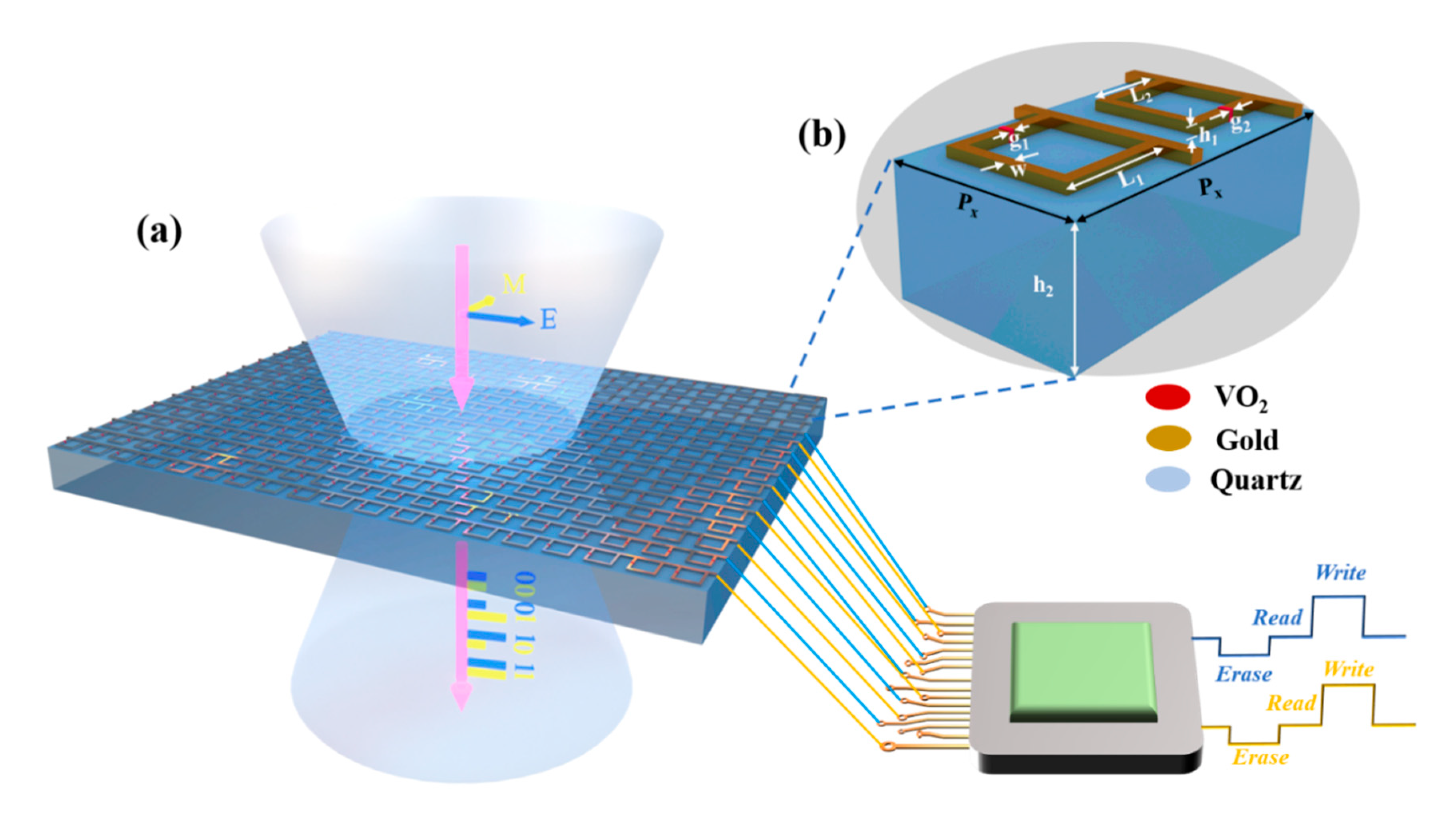
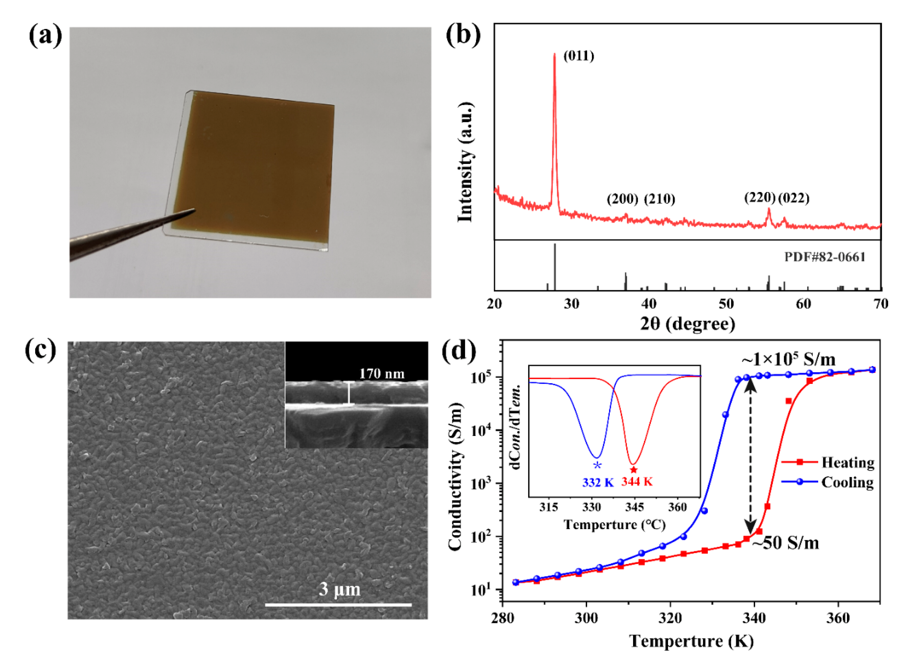
3. Materials and Devices

In this work, VO2 film samples were prepared by reactive radio frequency magnetron sputtering deposition. A metal vanadium target (purity of 99.9%, diameter of 2 inches, thickness of 5 mm, Zhongnuo New Materials (Beijing) Technology Co., Ltd., Beijing, China) was used to deposit VO2 film on silicon dioxide (SiO2) substrate. In the experiments, the distance between the target and the substrate was about 15 cm. The working gas, Ar with 99.999% purity, and the reaction gas, O2 with 99.999% purity, were introduced into the chamber with two mass flow controllers under a background vacuum of 8 × 10⁻⁴ Pa. The target was pre-sputtered for 5 min to eliminate the target surface contamination. During the deposition process, the Ar and O2 flow ratio was set to 60/2.4 sccm, and the total partial pressure of the gas in the chamber was ~0.7 Pa. The deposition temperature was maintained at 600 °C, the sputtering time was 40 min, and the sputtering power was 140 W. The optical photograph of the prepared film is shown in Figure 2a, which is a macroscopically transparent yellow-brown color.
The X-ray diffraction (XRD, D/MAX2500, Tokyo, Japan) patterns of the films were collected with Cu Kα as the source of radiation (λ = 0.15406 nm) under grazing incidence at an angle of 1.5°. As shown in Figure 2b, the peaks at approximately 27.98°, 37.12°, 42.34°, 55.64°, and 57.64° are indexed to diffractions from the (011), (200), (210), (220), and (022) planes of the monoclinic VO2 phase, respectively (JCPDS card no. 82-0661). The XRD pattern indicates good crystallinity with a preferred orientation for the film, and the relatively strong peak at approximately 27.98° indicates a preferred orientation of (011) for the films. The surface morphology of the film was observed with a field-emission scanning electron microscope (FEI Inspect F50, New York, NY, USA). The scanning electron microscopy (SEM) image of the VO2 film shown in Figure 2c illustrated that the VO2 film is compact without noticeable pores and consists of uniform, continuous nanoparticles whose size ranges from 50 to 90 nm with a mean value of approximately 70 nm. The inset at the upper right shows that the thickness of the prepared film is approximately 170 nm.
The electrical phase transition characteristics of VO2 thin films were studied by using the four-point probe method. The change in film sheet resistance with temperature was recorded, and the change in sample conductivity was calculated by combining the thickness of the film (Figure 2d). It can be seen from the figure that the conductivity value of the sample does not coincide in the process of heating and cooling, thus forming a hysteretic curve, which is one of the characteristics of the VO2 phase transition. When the temperature of the sample rose from 298 K to 363 K, the conductivity of the sample changed from 23 S/m to 1.2 × 10⁵ S/m. The maximum hysteresis interval exists at approximately 341 K. The heating and cooling curves correspond to conductivities of ~50 S/m and ~1 × 10⁵ S/m, respectively, spanning nearly 4 orders of magnitude. This change also indicates that our film prepared on SiO2 has a very high quality.

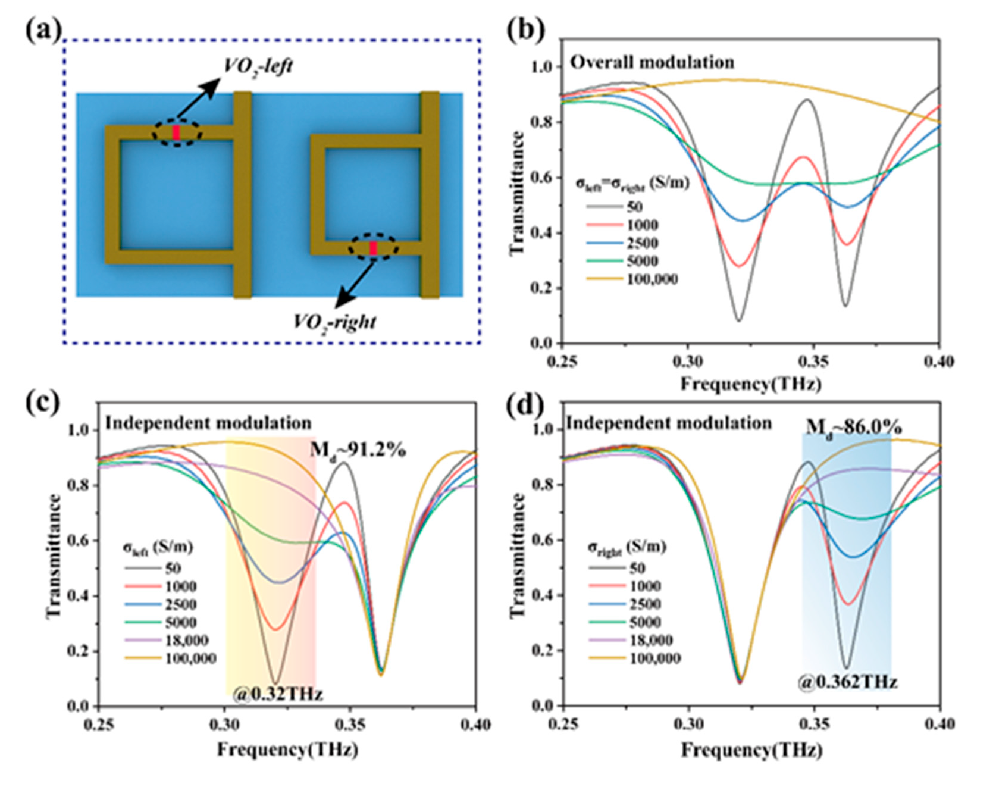
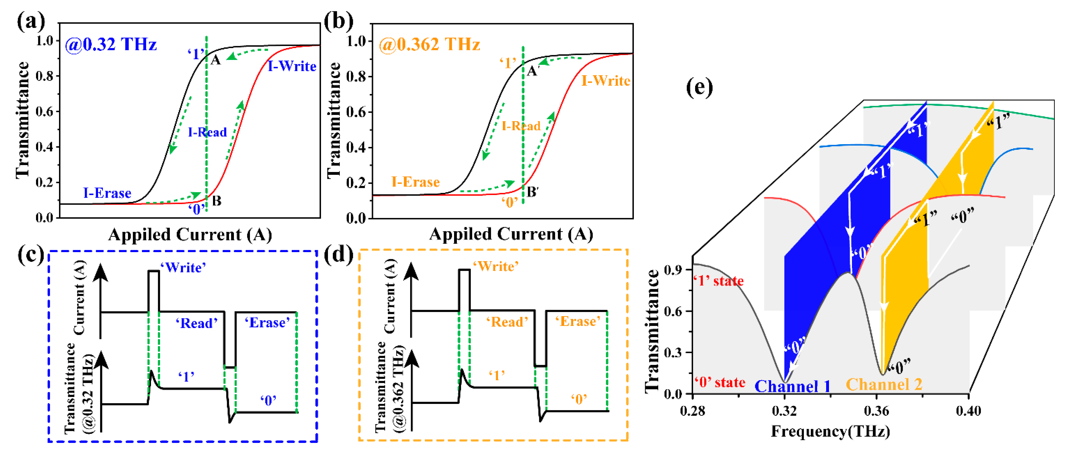
4. Results and Discussion

In this work, we simulated the transmission spectra of the hybrid metasurface under x-polarized incidence using the commercial software CST Microwave Studio. To study the influence of VO2 conductivity on the two designed terahertz channels, the changes in the transmittance at 0.32 THz and 0.362 THz in the target frequency band during the change of VO2 conductivity from 50 S/m to 1 × 10⁵ S/m were calculated, respectively. As shown in Figure 3a, VO2 patterns are distributed in the gaps of the left and right opening rings of different sizes, and the magnitude of the input current controls the degree of phase transformation. When VO2 patterns were in the insulating state (50 S/m), in the absence of external stimulation, the metasurface array had a resonance response at 0.32 THz and 0.362 THz, respectively. When the phase transformation degree of VO2 patterns was controlled to increase at the left and right sides, the transmittance at 0.32 THz increased from 8.1% to 92.6%, and at 0.362 THz, the transmittance increased from 13.0% to 90.0% (Figure 3b). Therefore, a high THz wave modulation depth can be obtained at two resonant peaks during the VO2 phase transition process.
In addition, the transmittance of the two resonant peaks can be adjusted independently, and the phase transformation of VO2 patterns in the gaps of the large or small opening rings can be controlled by feeding separately. As shown in Figure 3c,d, when VO2 (located on the left) in the gap of the large opening ring was stimulated by external current while VO2 at the small opening ring remained insulated, the obtained spectral transmittance at 0.32 THz increased gradually (from 8.1% to 92.6%), while the transmittance at 0.362 THz remained unchanged. Instead, the VO2 in the array with the small opening ring (on the right side of the whole) was excited, and the VO2 at the large opening ring remained insulated. The result was that the transmittance at 0.362 THz was modulated (from 13% to 92.8%), while the transmittance at 0.32 THz remained the same. The amplitude modulation depth (Md) is defined as M d = T max T min / T max . Therefore, approximately 91.2% and 86.0% of the modulation depth can be obtained at the 0.32 and 0.362 THz channels, respectively. VO2 has phase transformation hysteresis under external stimuli, such as thermal, electrical, photothermal and other conditions (Figure 2d), which can be used in memory devices. The cyclic hysteresis data of the conductance phase change of the VO2 thin film in Figure 2d were extracted and imported into CST for simulation calculation to obtain the corresponding transmission hysteresis curves at 0.32 THz and 0.362 THz, as shown in Figure 4a,b. Due to the optical hysteresis behaviors demonstrated, the meta-device can realize electric-controlled memory by utilizing the intrinsic hysteretic behavior of VO2. For example, looking at the transmission change of 0.32 THz in Figure 4a, the current at the maximum hysteretic point is selected as the “Read” current input. At that moment, a short current pulse is applied based on the “Read” current as the “Write” current, which can quickly cause the phase transition of VO2 and increase the transmission (as shown in the “Write” current pulse in Figure 4c). When returning to the “Read” current, the high transmission state can still be maintained (point A), that is, the “1” state at 0.32 THz. Here, for convenience, the high transmission state of terahertz is the “1” state, and the relatively low transmission state is the “0” state. If the input of the “Read” current is reduced rapidly over a brief period of time (as shown in the “Erase” current pulse in Figure 4c) then VO2 quickly recovers and results in a decrease in transmittance at 0.32 THz. When returning to the “Read” current, the low transmission state can be maintained (point B), that is, the “0” state at 0.32 THz. Therefore, the “0” and “1” states of 0.32 THz can be read and erased by encoding the current pulse, as shown in Figure 4b. Similarly, the resonance peak transmission at 0.362 THz can also be independently applied to the current for “0” and “1” state coding. Because the 0.32 THz and 0.362 THz bands can be modulated independently without interference, the two channels can be operated independently or combined to produce at least four different storage states of “00”, “01”, “10”, and “11”, which can significantly improve storage efficiency and flexibility. The four states here result from the cross-combination of the two channels. For example, “01” indicates a low transmission state at 0.32 THz and a high transmission state at 0.362 THz (Figure 4e). It is worth mentioning that the two-channel mode can be designed for 16 or more operating states when the contrast ratio is satisfactory (more details can be seen in Figure S1 of the Supporting Information). Currently, VO2-based terahertz storage devices are generally available in a single-channel mode. Therefore, based on this design, storage efficiency and flexibility can be significantly improved.
To further understand the mechanism of the influence of VO2 conductivity change on resonance, the electric field and current distribution on the structure surface under different storage states (“00”, “01”, “10”, and “11”) are shown in Figure 5 and Figure 6, respectively. At 0.32 THz, when VO2 patterns in the gaps between the large and small rings were insulating, the electric field concentrated on the opening of the large ring, and a strong ring current was formed on the surface (Figure 5a and Figure 6a). At this moment, the resistance of the VO2 patterns was large and equivalent to that of a capacitor, which is a typical L-C resonant mode. Consequently, the transmittance at 0.32 THz was low. Similarly, a ring current was also formed on the surface of the small ring, but the structure size was small, and the resonance caused by it appeared at 0.362 THz (Figure 5b and Figure 6b). While the VO2 patterns embedded in the large ring openings remained insulated, the conductivity of the VO2 patterns in the small ring openings began to rise in response to environmental stimuli. The electric field intensity at the opening of the small rings decreased and the surface ring current decreased, resulting in an increase in the transmission intensity at 0.362 THz. However, at 0.32 THz, there was still a strong ring current on the surface of the large rings, indicating that there was still a strong L-C resonance, and so 0.32 THz was in the low transmission state. That is, the device was now in the “01” state.
In contrast, Figure 5e,f and Figure 6e,f show the electric field distribution in the “10” state. In this case, there was a substantial ring current on the surface of the small rings at 0.362 THz and a concentration of electric field at the openings, so the transmission at 0.362 THz was low. While the VO2 conductivity at the large rings increased, the capacitance property at the opening weakened, and the transmittance at 0.32 THz increased. When the VO2 patterns in the large and small opening rings underwent phase transformation, there was no electric field concentration on the surface of the two structures, and the surface current was relatively weak, as shown in Figure 5g,h and Figure 6g,h. This situation corresponds to the “11” state.

5. Conclusions

In this work, we have demonstrated a tunable memory meta-device based on the IMT of VO2, in which large and small splitting rings are arranged alternatively, and VO2 patterns are embedded in the opening part of the splitting ring. Under the applied coding current, the transmittance of 0.32 THz and 0.362 THz can be controlled independently, and modulation depths of 91.2% and 86.0% can be obtained, respectively. Most importantly, based on the intrinsic phase change memory effect of VO2, at least four storage states of “00”, “01”, “10” and “11” can be attained by encoding the high and low terahertz transmission states at the 0.32 and 0.362 THz channels. In addition, based on this design, the storage capacity can be increased exponentially with the number of coded channels. Compared with the previous single-channel storage mode, the design can significantly improve storage efficiency and flexibility. Due to these characteristics, the proposed meta-device may provide a reference for the design of tunable devices, terahertz switches and photonic storage devices in the terahertz range.

Supplementary Materials

The following are available online at https://www.mdpi.com/article/10.3390/nano11123409/s1, Figure S1: Demonstration of 16 storage status functions in two-channel mode.

Author Contributions

X.L. and C.Z. conceived the research, undertook the simulations and analysis, and wrote the manuscript. B.D., H.Z., Q.S., L.T. and Y.S. contributed to the analysis and the manuscript review. W.H. and Q.C. supervised the project. All authors discussed the results, performed data analysis and explanation, wrote the manuscript, and revised it. All authors have read and agreed to the published version of the manuscript.

Funding

This work was supported in part by the National Key Research and Development Program of China (2018YFA0701904, 2017YFA0700201, 2017YFA0700202, 2017YFA0700203, and 2020YFA0710100), the National Natural Science Foundation of China (62101394, 61722106, 61731010 and 61771327), the Fundamental Research Funds for the Central Universities (WUT: 2021IVA064).

Institutional Review Board Statement

Not applicable.

Informed Consent Statement

Not applicable.

Data Availability Statement

The data presented in this study are available on request from the corresponding author.

Conflicts of Interest

The authors declare no conflict of interest.

References

  1. Rappaport, T.S.; Xing, Y.; Kanhere, O.; Ju, S.; Madanayake, A.; Mandal, S.; Alkhateeb, A.; Trichopoulos, G.C. Wireless communications and applications above 100 GHz: Opportunities and challenges for 6G and beyond. IEEE Access 2019, 7, 78729–78757. [Google Scholar] [CrossRef]
  2. Chen, X.; Liu, X.; Guo, X.; Chen, S.; Hu, H.; Nikulina, E.; Ye, X.; Yao, Z.; Bechtel, H.A.; Martin, M.C.; et al. THz near-field imaging of extreme subwavelength metal structures. ACS Photonics 2020, 7, 687–694. [Google Scholar] [CrossRef]
  3. Zhong, S. Progress in terahertz nondestructive testing: A review. Front. Mech. Eng. 2019, 14, 273–281. [Google Scholar] [CrossRef]
  4. Wang, L.; Zhang, Y.; Guo, X.; Chen, T.; Liang, H.; Hao, X.; Hou, X.; Kou, W.; Zhao, Y.; Zhou, T.; et al. A Review of THz Modulators with Dynamic Tunable Metasurfaces. Nanomaterials 2019, 9, 965. [Google Scholar] [CrossRef] [Green Version]
  5. Bao, L.; Cui, T.J. Tunable, reconfigurable, and programmable metamaterials. Microw. Opt. Technol. Lett. 2020, 62, 9–32. [Google Scholar] [CrossRef]
  6. Jeong, Y.-G.; Bahk, Y.-M.; Kim, D.-S. Dynamic terahertz plasmonics enabled by phase-change materials. Adv. Opt. Mater. 2020, 8, 1900548. [Google Scholar] [CrossRef]
  7. Zheng, C.; Li, J.; Wang, G.; Wang, S.; Li, J.; Zhao, H.; Zang, H.; Zhang, Y.; Zhang, Y.; Yao, J. Fine manipulation of terahertz waves via all-silicon metasurfaces with an independent amplitude and phase. Nanoscale 2021, 13, 5809–5816. [Google Scholar] [CrossRef] [PubMed]
  8. Lou, J.; Liang, J.; Yu, Y.; Ma, H.; Yang, R.; Fan, Y.; Wang, G.; Cai, T. Silicon-Based Terahertz Meta-Devices for Electrical Modulation of Fano Resonance and Transmission Amplitude. Adv. Opt. Mater. 2020, 8, 2000449. [Google Scholar] [CrossRef]
  9. Guo, J.; Wang, T.; Zhao, H.; Wang, X.; Feng, S.; Han, P.; Sun, W.; Ye, J.; Situ, G.; Chen, H.-T.; et al. Reconfigurable terahertz metasurface pure phase holograms. Adv. Opt. Mater. 2019, 7, 1801696. [Google Scholar] [CrossRef]
  10. Yao, B.; Liu, Y.; Huang, S.-W.; Choi, C.; Xie, Z.; Flor Flores, J.; Wu, Y.; Yu, M.; Kwong, D.-L.; Huang, Y.; et al. Broadband gate-tunable terahertz plasmons in graphene heterostructures. Nat. Photonics 2018, 12, 22–28. [Google Scholar] [CrossRef] [Green Version]
  11. Zhang, C.; Long, C.; Yin, S.; Song, R.G.; Zhang, B.H.; Zhang, J.W.; He, D.P.; Cheng, Q. Graphene-based anisotropic polarization meta-filter. Mater. Des. 2021, 206, 109768. [Google Scholar] [CrossRef]
  12. Zhang, C.; Yin, S.; Long, C.; Dong, B.W.; He, D.; Cheng, Q.; Cheng, Q. Hybrid Metamaterial Absorber for Ultra-Low and Dual-Broadband Absorption. Opt. Express 2021, 29, 14078–14086. [Google Scholar] [CrossRef]
  13. He, X.; Lin, F.; Liu, F.; Shi, W. Tunable strontium titanate terahertz all-dielectric metamaterials. J. Phys. D Appl. Phys. 2020, 53, 155105. [Google Scholar] [CrossRef]
  14. Dong, B.; Ma, H.; Wang, J.; Shi, P.; Li, J.; Zhu, L.; Lou, J.; Feng, M.; Qu, S. A thermally tunable THz metamaterial frequency-selective surface based on barium strontium titanate thin film. J. Phys. D Appl. Phys. 2018, 52, 045301. [Google Scholar] [CrossRef]
  15. Feng, T.; Huang, W.; Zhu, H.; Lu, X.; Das, S.; Shi, Q. Optical-Transparent Self-Assembled MXene Film with High-Efficiency Terahertz Reflection Modulation. ACS Appl. Mater. Interfaces 2021, 13, 10574–10582. [Google Scholar] [CrossRef] [PubMed]
  16. Choi, G.; Shahzad, F.; Bahk, Y.-M.; Jhon, Y.M.; Park, H.; Alhabeb, M.; Anasori, B.; Kim, D.-S.; Koo, C.M.; Gogotsi, Y.; et al. Enhanced terahertz shielding of MXenes with nano-metamaterials. Adv. Opt. Mater. 2018, 6, 1701076. [Google Scholar] [CrossRef]
  17. Pitchappa, P.; Kumar, A.; Prakash, S.; Jani, H.; Venkatesan, T.; Singh, R. Chalcogenide phase change material for active terahertz photonics. Adv. Mater. 2019, 31, 1808157. [Google Scholar] [CrossRef] [Green Version]
  18. Zhao, Y.; Zhang, Y.; Shi, Q.; Liang, S.; Huang, W.; Kou, W.; Yang, Z. Dynamic photoinduced controlling of the large phase shift of terahertz waves via vanadium dioxide coupling nanostructures. ACS Photonics 2018, 5, 3040–3050. [Google Scholar]
  19. Liu, X.; Wang, Q.; Zhang, X.; Li, H.; Xu, Q.; Xu, Y.; Chen, X.; Li, S.; Liu, M.; Tian, Z.; et al. Thermally dependent dynamic meta-holography using a vanadium dioxide integrated metasurface. Adv. Opt. Mater. 2019, 7, 1900175. [Google Scholar] [CrossRef]
  20. Danila, O. Polyvinylidene Fluoride-Based Metasurface for High-Quality Active Switching and Spectrum Shaping in the Terahertz G-Band. Polymers 2021, 13, 1860. [Google Scholar] [CrossRef]
  21. Dănilă, O.; Mănăilă-Maximean, D.; Bărar, A.; Loiko, V.A. Non-Layered Gold-Silicon and All-Silicon Frequency-Selective Metasurfaces for Potential Mid-Infrared Sensing Applications. Sensors 2021, 21, 5600. [Google Scholar] [CrossRef] [PubMed]
  22. Lee, D.; Chung, B.; Shi, Y.; Kim, G.-Y.; Campbell, N.; Xue, F.; Song, K.; Choi, S.-Y.; Podkaminer, J.P.; Kim, T.H.; et al. Isostructural metal-insulator transition in VO2. Science 2018, 362, 1037–1040. [Google Scholar] [CrossRef] [Green Version]
  23. Shi, Q.; Huang, W.; Zhang, Y.; Yan, J.; Zhang, Y.; Mao, M.; Zhang, Y.; Tu, M. Giant phase transition properties at terahertz range in VO2 films deposited by sol–gel method. ACS Appl. Mater. Interfaces 2011, 3, 3523–3527. [Google Scholar] [CrossRef]
  24. Nakano, M.; Shibuya, K.; Okuyama, D.; Hatano, T.; Ono, S.; Kawasaki, M.; Iwasa, Y.; Tokura, Y. Collective bulk carrier delocalization driven by electrostatic surface charge accumulation. Nature 2012, 487, 459–462. [Google Scholar] [CrossRef]
  25. Jeong, J.; Aetukuri, N.; Graf, T.; Schladt, T.D.; Samant, M.G.; Parkin, S.S.P. Suppression of metal-insulator transition in VO2 by electric field–induced oxygen vacancy formation. Science 2013, 339, 1402–1405. [Google Scholar] [PubMed]
  26. Zhai, Z.-H.; Chen, S.-C.; Du, L.-H.; Zhong, S.-C.; Huang, W.; Li, Z.-R.; Schneider, H.; Shi, Q.; Zhu, L.-G. Giant impact of self-photothermal on light-induced ultrafast insulator-to-metal transition in VO2 nanofilms at terahertz frequency. Opt. Express 2018, 26, 28051–28066. [Google Scholar] [CrossRef] [PubMed]
  27. Lee, D.; Lee, J.; Song, K.; Xue, F.; Choi, S.-Y.; Ma, Y.; Podkaminer, J.; Liu, D.; Liu, S.-C.; Chung, B.; et al. Sharpened VO2 Phase Transition via Controlled Release of Epitaxial Strain. Nano Lett. 2017, 17, 5614–5619. [Google Scholar] [CrossRef]
  28. Driscoll, T.; Kim, H.-T.; Chae, B.-G.; Di Ventra, M.; Basov, D.N. Phase-Transition Driven Memristive System. Appl. Phys. Lett. 2009, 95, 043503. [Google Scholar] [CrossRef] [Green Version]
  29. Bae, S.-H.; Lee, S.; Koo, H.; Lin, L.; Jo, B.H.; Park, C.; Wang, Z.L. The memristive properties of a single VO2 nanowire with switching controlled by self-heating. Adv. Mater. 2013, 25, 5098–5103. [Google Scholar] [CrossRef]
  30. Yuan, H.-K.; Chen, S.-C.; Zhu, L.-G.; Zhai, Z.-H.; Du, L.-H.; Li, J. All optically-controlled multifunctional VO2 memory device for terahertz waves. In Proceedings of the 2019 International Conference on Optical Instruments and Technology: IRMMW-THz Technologies and Applications, Beijing, China, 26–28 October 2019; Volume 11441, p. 114410K. [Google Scholar]
  31. Coy, H.; Cabrera, R.; Sepúlveda, N.; Fernández, F.E. Optoelectronic and all-optical multiple memory states in vanadium dioxide. J. Appl. Phys. 2010, 108, 113115. [Google Scholar] [CrossRef] [Green Version]
  32. Pellegrino, L.; Manca, N.; Kanki, T.; Tanaka, H.; Biasotti, M.; Bellingeri, E.; Siri, A.S.; Marré, D. Multistate memory devices based on free-standing VO2/TiO2 microstructures driven by Joule self-Heating. Adv. Mater. 2012, 24, 2929–2934. [Google Scholar] [CrossRef]
  33. Driscoll, T.; Kim, H.-T.; Chae, B.-G.; Kim, B.-J.; Lee, Y.-W.; Jokerst, N.M.; Palit, S.; Smith, D.R.; Ventra, M.D.; Basov, D.N. Memory metamaterials. Science 2009, 325, 1518–1521. [Google Scholar] [CrossRef] [Green Version]
  34. Cai, H.; Chen, S.; Zou, C.; Huang, Q.; Liu, Y.; Hu, X.; Fu, Z.; Zhao, Y.; He, H.; Lu, Y. Multifunctional hybrid metasurfaces for dynamic tuning of terahertz waves. Adv. Opt. Mater. 2018, 6, 1800257. [Google Scholar] [CrossRef]
  35. Liu, L.; Kang, L.; Mayer, T.S.; Werner, D.H. Hybrid metamaterials for electrically triggered multifunctional control. Nat Commun 2016, 7, 13236. [Google Scholar] [CrossRef]
  36. Qazilbash, M.M.; Brehm, M.; Chae, B.-G.; Ho, P.-C.; Andreev, G.O.; Kim, B.-J.; Yun, S.J.; Balatsky, A.V.; Maple, M.B.; Keilmann, F.; et al. Mott transition in VO2 revealed by infrared spectroscopy and nano-imaging. Science 2007, 318, 1750–1753. [Google Scholar] [CrossRef] [Green Version]
  37. Jepsen, P.U.; Fischer, B.M.; Thoman, A.; Helm, H.; Suh, J.Y.; Lopez, R.; Haglund, R.F. Metal-insulator phase transition in a VO2 thin film observed with terahertz spectroscopy. Phys. Rev. B 2006, 74, 205103. [Google Scholar] [CrossRef] [Green Version]
  38. Bruggeman, D.A.G. The calculation of various physical constants of heterogeneous substances. I. The dielectric constants and conductivities of mixtures composed of isotropic substances. Ann. Phys. 1935, 416, 636–791. [Google Scholar] [CrossRef]
  39. Hood, P.J.; DeNatale, J.F. Millimeter-wave Dielectric Properties of Epitaxial Vanadium Dioxide Thin Films. J. Appl. Phys. 1991, 70, 376–381. [Google Scholar] [CrossRef]
  40. Choi, H.S.; Ahn, J.S.; Jung, J.H.; Noh, T.W.; Kim, D.H. Mid-Infrared Properties of a VO2 Film near the Metal-Insulator Transition. Phys. Rev. B 1996, 54, 4621. [Google Scholar] [CrossRef]
  41. Driscoll, T.; Palit, S.; Qazilbash, M.M.; Brehm, M.; Keilmann, F.; Chae, B.-G.; Yun, S.-J.; Kim, H.-T.; Cho, S.Y.; Jokerst, N.M.; et al. Dynamic Tuning of an Infrared Hybrid-Metamaterial Resonance Using Vanadium Dioxide. Appl. Phys. Lett. 2008, 93, 024101. [Google Scholar] [CrossRef]
  42. Shabanpour, J. Programmable anisotropic digital metasurface for independent manipulation of dual-polarized THz waves based on a voltage-controlled phase transition of VO2 microwires. J. Mater. Chem. C 2020, 8, 7189–7199. [Google Scholar] [CrossRef] [Green Version]
  43. Zhu, H.-F.; Du, L.-H.; Li, J.; Shi, Q.-W.; Peng, B.; Li, Z.-R.; Huang, W.-X.; Zhu, L.-G. Near-perfect terahertz wave amplitude modulation enabled by impedance matching in VO2 thin films. Appl. Phys. Lett. 2018, 112, 081103. [Google Scholar] [CrossRef]
Figure 1. Schematic diagram of the two-channel THz memory storage device based on vanadium dioxide. (a) Schematic diagram of a reconfigurable metasurface in which two electrodes input a programmable current to independently control the THz transmission state of two frequency channels. (b) Unit cell of the metasurface is depicted in the inset, where Px = 220 μm, Py = 120 μm, L1 = 80 μm, L2 = 70 μm, g1 = 4 μm, g2 = 4 μm, h1 = 0.2 μm, and h2 = 200 μm.
Nanomaterials 11 03409 g001
Figure 2. Preparation and characterization of VO2 films. (a) Optical image of the VO2 thin film prepared by magnetron sputtering. (b) XRD pattern and (c) SEM image of the VO2 film. (d) Conductivity-temperature curves for VO2 films grown on SiO2 substrate.
Nanomaterials 11 03409 g002
Figure 3. Effect of conductivity variation on terahertz transmittance at resonant peak at two frequency bands during VO2 phase transition. (a) In the top view of the unit structure, two VO2 pieces are independently embedded in the large and small opening rings. (b) When the conductance of the VO2 film on the left and right sides of the unit changes simultaneously, the terahertz transmittance at the resonant peak of 0.25 THz and 0.362 THz increases synchronously. (c,d) Keep the VO2 conductivity on one side constant and the VO2 on the other side gradually changes. (c) Right side and (d) left side VO2 conductivity unchanged.
Nanomaterials 11 03409 g003
Figure 4. Effect of conductivity variation on terahertz transmittance at resonant peak at two frequency bands during VO2 phase transition. (a) In the top view of the unit structure, two VO2 pieces are independently embedded in the large and small opening rings. (b) When the conductance of the VO2 film on the left and right sides of the unit changes simultaneously, the terahertz transmittance at the resonant peak of 0.25 THz and 0.362 THz increases synchronously. (c,d) Keep the VO2 conductivity on one side constant and the VO2 on the other side gradually changes. (c) Left side and (d) right side VO2 conductivity unchanged. (e) Schematic diagram of the two channels being stored independently.
Nanomaterials 11 03409 g004
Figure 5. At 0.32 THz and 0.362 THz, respectively, the electric field distribution diagram of the cell structure in different storage states. (a,b) σleft = σright = 50 S/m (“00” state); (c,d) σleft = 50 S/m, σright = 100,000 S/m (“01” state); (e,f) σleft = 100,000 S/m, σright = 50 S/m (“10” state); (g,h) σleft = σright = 100,000 S/m (“11” state).
Nanomaterials 11 03409 g005
Figure 6. The 0.32 THz and 0.362 THz values, respectively, the surface current distribution diagram of the cell structure in different storage states. (a,b) σleft = σright = 50 S/m (“00” state); (c,d) σleft = 50 S/m, σright = 100,000 S/m (“01” state); (e,f) σleft = 100,000 S/m, σright = 50 S/m (“10” state); (g,h) σleft = σright = 100,000 S/m (“11” state).
Nanomaterials 11 03409 g006
Publisher’s Note: MDPI stays neutral with regard to jurisdictional claims in published maps and institutional affiliations.

