
Hybrid Metal-Dielectric-Metal Sandwiches for SERS Applications

 ,
,  ,
,  and
and 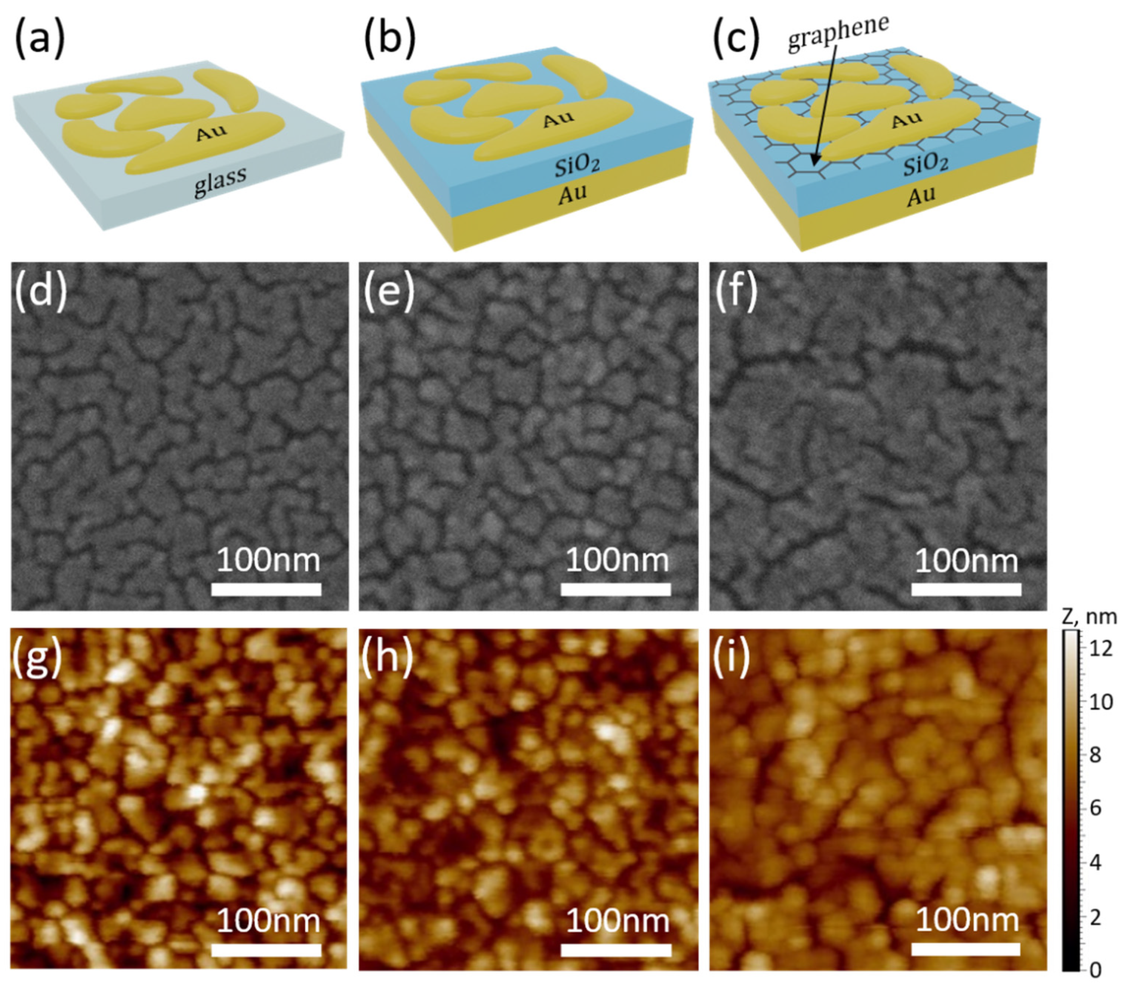
Abstract
:1. Introduction
2. Materials and Methods
2.1. Sample Fabrication
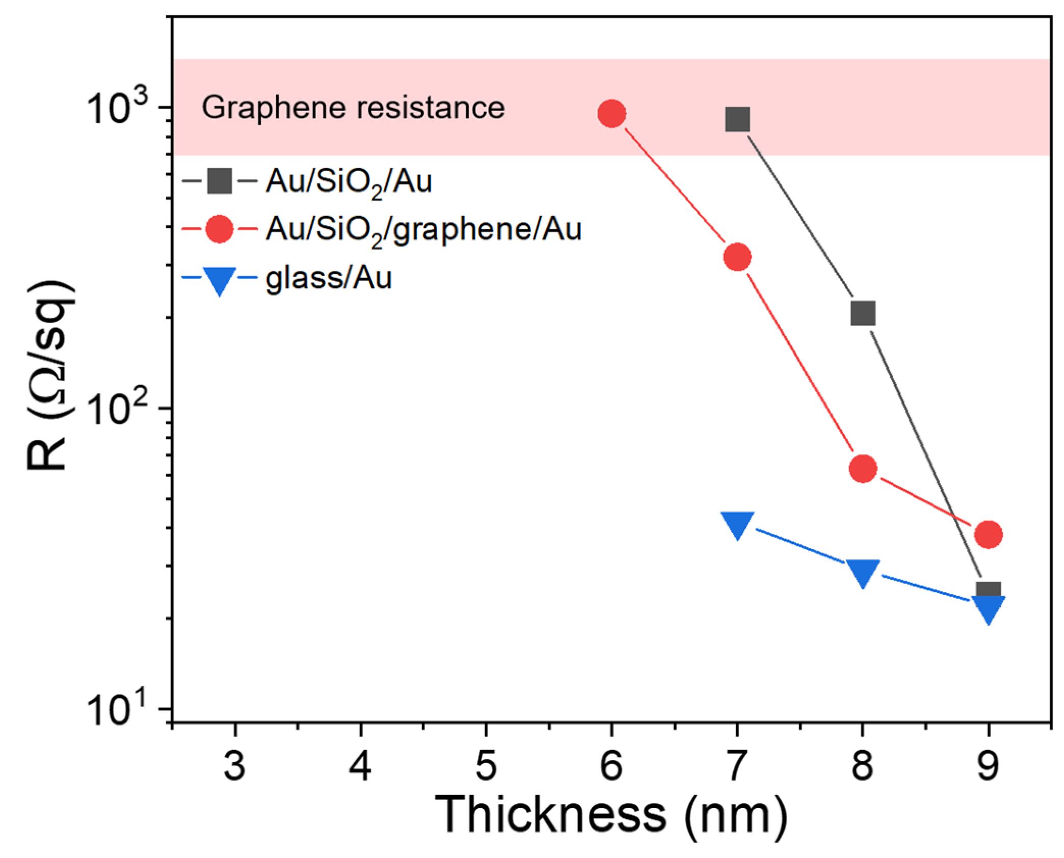
2.2. Electrical Measurements, Scanning Electron, and Atomic Force Microscopy
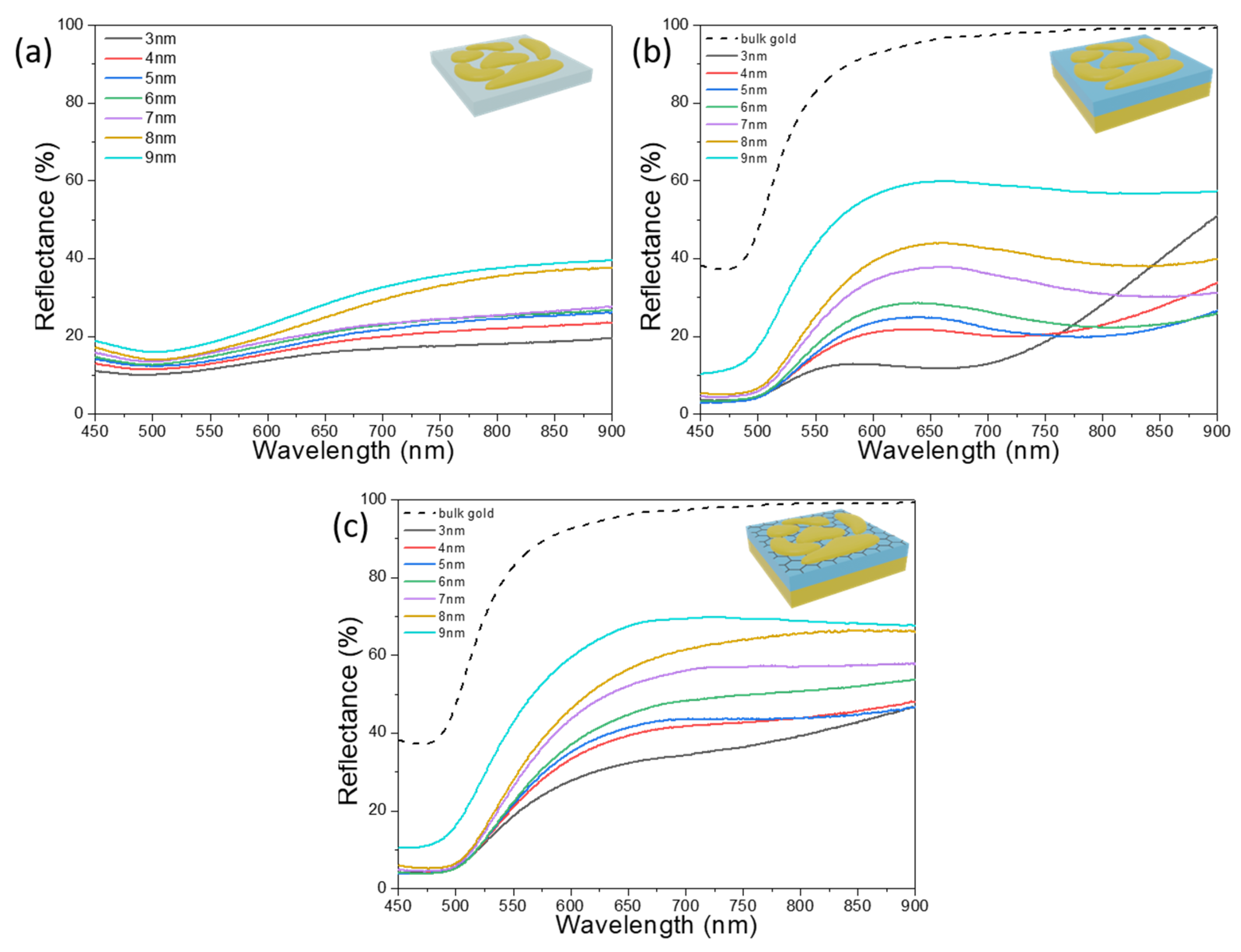
2.3. Reflection Analysis
2.4. Ellipsometry
2.5. Numerical Calculations of the Reflection and Absorption Spectra
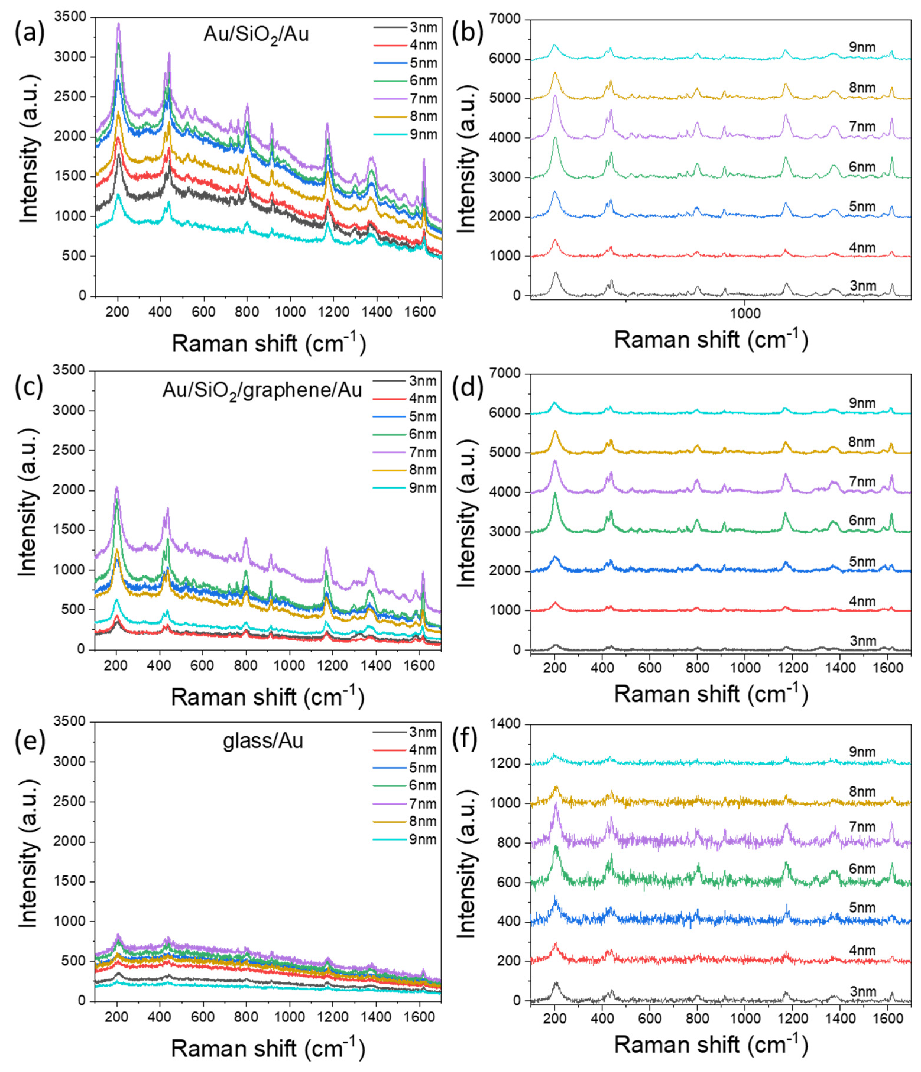
2.6. Raman Measurements
3. Results
4. Conclusions
Supplementary Materials
Author Contributions
Funding
Institutional Review Board Statement
Informed Consent Statement
Data Availability Statement
Acknowledgments
Conflicts of Interest
References
- Langer, J.; Jimenez de Aberasturi, D.; Aizpurua, J.; Alvarez Puebla, R.A.; Auguie, B.; Baumberg, J.J.; Bazan, G.C.; Bell, S.E.J.; Boisen, A.; Brolo, A.G.; et al. Present and Future of Surface-Enhanced Raman Scattering. ACS Nano 2020, 14, 28–117. [Google Scholar] [CrossRef] [Green Version]
- Kneipp, K.; Wang, Y.; Kneipp, H.; Perelman, L.T.; Itzkan, I.; Dasari, R.R.; Feld, M.S. Single Molecule Detection Using Surface-Enhanced Raman Scattering (SERS). Phys. Rev. Lett. 1997, 78, 1667–1670. [Google Scholar] [CrossRef] [Green Version]
- Beermann, J.; Novikov, S.M.; Albrektsen, O.; Nielsen, M.G.; Bozhevolnyi, S.I. Surface-enhanced Raman imaging of fractal shaped periodic metal nanostructures. J. Opt. Soc. Am. B 2009, 26, 2370–2376. [Google Scholar] [CrossRef]
- Gramotnev, D.K.; Bozhevolnyi, S.I. Plasmonics beyond the diffraction limit. Nat. Photonics 2010, 4, 83–91. [Google Scholar] [CrossRef]
- Maier, S.A. Plasmonics: Fundamentals and Applications; Springer Science + Business Media: Berlin, Germany, 2007; ISBN 9780387378251. [Google Scholar]
- Lal, S.; Link, S.; Halas, N.J. Nano-optics from sensing to waveguiding. Nat. Photonics 2007, 1, 641–648. [Google Scholar] [CrossRef]
- Evlyukhin, A.B.; Kuznetsov, A.I.; Novikov, S.M.; Beermann, J.; Reinhardt, C.; Kiyan, R.; Bozhevolnyi, S.I.; Chichkov, B.N. Optical properties of spherical gold mesoparticles. Appl. Phys. B 2012, 106, 841–848. [Google Scholar] [CrossRef]
- Seal, K.; Genov, D.A.; Sarychev, A.K.; Noh, H.; Shalaev, V.M.; Ying, Z.C.; Zhang, X.; Cao, H. Coexistence of localized and delocalized surface plasmon modes in percolating metal films. Phys. Rev. Lett. 2006, 97, 206103. [Google Scholar] [CrossRef]
- Novikov, S.M.; Beermann, J.; Frydendahl, C.; Stenger, N.; Coello, V.; Mortensen, N.A.; Bozhevolnyi, S.I. Enhancement of two-photon photoluminescence and SERS for low-coverage gold films. Opt. Express 2016, 24, 16743–16751. [Google Scholar] [CrossRef] [PubMed] [Green Version]
- Shiohara, A.; Novikov, S.M.; Solís, D.M.; Taboada, J.M.; Obelleiro, F.; Liz-Marzán, L.M. Plasmon Modes and Hot Spots in Gold Nanostar–Satellite Clusters. J. Phys. Chem. C 2015, 119, 10836–10843. [Google Scholar] [CrossRef] [Green Version]
- Moskovits, M. Spot the hotspot. Nature 2011, 469, 307–308. [Google Scholar] [CrossRef]
- Novikov, S.M.; Frydendahl, C.; Beermann, J.; Zenin, V.A.; Stenger, N.; Coello, V.; Mortensen, N.A.; Bozhevolnyi, S.I. White Light Generation and Anisotropic Damage in Gold Films near Percolation Threshold. ACS Photonics 2017, 4, 1207–1215. [Google Scholar] [CrossRef] [Green Version]
- Ducourtieux, S.; Podolskiy, V.A.; Grésillon, S.; Buil, S.; Berini, B.; Gadenne, P.; Boccara, A.C.; Rivoal, J.C.; Bragg, W.D.; Banerjee, K.; et al. Near-field optical studies of semicontinuous metal films. Phys. Rev. B Condens. Matter 2001, 64, 165403. [Google Scholar] [CrossRef] [Green Version]
- De Zuani, S.; Peterseim, T.; Berrier, A.; Gompf, B.; Dressel, M. Second harmonic generation enhancement at the percolation threshold. Appl. Phys. Lett. 2014, 104, 241109. [Google Scholar] [CrossRef]
- Tatarkin, D.; Yakubovsky, D.; Ermolaev, G.; Stebunov, Y.; Voronov, A.; Arsenin, A.; Volkov, V.; Novikov, S. Surface-Enhanced Raman Spectroscopy on Hybrid Graphene/Gold Substrates Near the Percolation Threshold. Nanomaterials 2020, 10, 164. [Google Scholar] [CrossRef] [Green Version]
- Liszewska, M.; Budner, B.; Norek, M.; Jankiewicz, B.J.; Nyga, P. Revisiting semicontinuous silver films as surface-enhanced Raman spectroscopy substrates. Beilstein. J. Nanotechnol. 2019, 10, 1048–1055. [Google Scholar] [CrossRef]
- Fateixa, S.; Nogueira, H.I.S.; Trindade, T. Hybrid nanostructures for SERS: Materials development and chemical detection. Phys. Chem. Chem. Phys. 2015, 17, 21046–21071. [Google Scholar] [CrossRef] [PubMed]
- Eremina, O.E.; Kapitanova, O.O.; Goodilin, E.A.; Veselova, I.A. Silver-chitosan nanocomposite as a plasmonic platform for SERS sensing of polyaromatic sulfur heterocycles in oil fuel. Nanotechnology 2020, 31, 225503. [Google Scholar] [CrossRef]
- Søndergaard, T.; Jung, J.; Bozhevolnyi, S.I.; Della Valle, G. Theoretical analysis of gold nano-strip gap plasmon resonators. New J. Phys. 2008, 10, 105008. [Google Scholar] [CrossRef]
- Jung, J.; Søndergaard, T.; Bozhevolnyi, S.I. Gap plasmon-polariton nanoresonators: Scattering enhancement and launching of surface plasmon polaritons. Phys. Rev. B 2009, 79, 035401. [Google Scholar] [CrossRef]
- Nielsen, M.G.; Gramotnev, D.K.; Pors, A.; Albrektsen, O.; Bozhevolnyi, S.I. Continuous layer gap plasmon resonators. Opt. Express 2011, 19, 19310–19322. [Google Scholar] [CrossRef]
- Baumberg, J.J.; Aizpurua, J.; Mikkelsen, M.H.; Smith, D.R. Extreme nanophotonics from ultrathin metallic gaps. Nat. Mater. 2019, 18, 668–678. [Google Scholar] [CrossRef]
- Lordan, F.; Damm, S.; Kennedy, E.; Mallon, C.; Forster, R.; Keyes, T.; Rice, J.H. The Effect of Ag Nanoparticles on Surface-Enhanced Luminescence from Au Nanovoid Arrays. Plasmonics 2013, 8, 1567–1575. [Google Scholar] [CrossRef] [Green Version]
- Lai, H.; Xu, F.; Zhang, Y.; Wang, L. Recent progress on graphene-based substrates for surface-enhanced Raman scattering applications. J. Mater. Chem. B Mater. Biol. Med. 2018, 6, 4008–4028. [Google Scholar] [CrossRef]
- Wang, Z.; Wu, S.; Colombi Ciacchi, L.; Wei, G. Graphene-based nanoplatforms for surface-enhanced Raman scattering sensing. Analyst 2018, 143, 5074–5089. [Google Scholar] [CrossRef]
- Xie, L.; Ling, X.; Fang, Y.; Zhang, J.; Liu, Z. Graphene as a substrate to suppress fluorescence in resonance Raman spectroscopy. J. Am. Chem. Soc. 2009, 131, 9890–9891. [Google Scholar] [CrossRef]
- Fan, H.; Wang, L.; Zhao, K.; Li, N.; Shi, Z.; Ge, Z.; Jin, Z. Fabrication, mechanical properties, and biocompatibility of graphene-reinforced chitosan composites. Biomacromolecules 2010, 11, 2345–2351. [Google Scholar] [CrossRef] [PubMed]
- Moreau, A.; Ciracì, C.; Mock, J.; Hill, R.T.; Wang, Q.; Wiley, B.J.; Chilkoti, A.; Smith, D.R. Controlled-reflectance surfaces with film-coupled colloidal nanoantennas. Nature 2012, 492, 86–89. [Google Scholar] [CrossRef] [Green Version]
- Lu, Y.; Dong, W.; Chen, Z.; Pors, A.; Wang, Z.; Bozhevolnyi, S.I. Gap-plasmon based broadband absorbers for enhanced hot-electron and photocurrent generation. Sci. Rep. 2016, 6, 30650. [Google Scholar] [CrossRef] [PubMed] [Green Version]
- Nielsen, M.G.; Pors, A.; Albrektsen, O.; Bozhevolnyi, S.I. Efficient absorption of visible radiation by gap plasmon resonators. Opt. Express 2012, 20, 13311–13319. [Google Scholar] [CrossRef] [Green Version]
- Guo, Y.; Jiang, S.; Chen, X.; Mattei, M.; Dieringer, J.A.; Ciraldo, J.P.; Van Duyne, R.P. Using a Fabry−Perot Cavity to Augment the Enhancement Factor for Surface-Enhanced Raman Spectroscopy and Tip-Enhanced Raman Spectroscopy. J. Phys. Chem. C 2018, 122, 14865–14871. [Google Scholar] [CrossRef]
- Shoute, L.C.T.; Bergren, A.J.; Mahmoud, A.M.; Harris, K.D.; McCreery, R.L. Optical Interference Effects in the Design of Substrates for Surface-Enhanced Raman Spectroscopy. Appl. Spectrosc. 2009, 63, 133–140. [Google Scholar] [CrossRef]
- Her, M.; Beams, R.; Novotny, L. Graphene transfer with reduced residue. Phys. Lett. A 2013, 377, 1455–1458. [Google Scholar] [CrossRef] [Green Version]
- Cho, Y.J.; Nguyen, N.V.; Richter, C.A.; Ehrstein, J.R.; Lee, B.H.; Lee, J.C. Spectroscopic ellipsometry characterization of high-k dielectric HfO2 thin films and the high-temperature annealing effects on their optical properties. Appl. Phys. Lett. 2002, 80, 1249–1251. [Google Scholar] [CrossRef] [Green Version]
- El-Sayed, M.A.; Ermolaev, G.A.; Voronin, K.V.; Romanov, R.I.; Tselikov, G.I.; Yakubovsky, D.I.; Doroshina, N.V.; Nemtsov, A.B.; Solovey, V.R.; Voronov, A.A.; et al. Optical Constants of Chemical Vapor Deposited Graphene for Photonic Applications. Nanomaterials 2021, 11, 1230. [Google Scholar] [CrossRef]
- Johnson, P.B.; Christy, R.W. Optical Constants of the Noble Metals. Phys. Rev. B 1972, 6, 4370. [Google Scholar] [CrossRef]
- Kapitanova, O.O.; Kataev, E.Y.; Usachov, D.Y.; Sirotina, A.P.; Belova, A.I.; Sezen, H.; Amati, M.; Al-Hada, M.; Gregoratti, L.; Barinov, A.; et al. Laterally Selective Oxidation of Large-Scale Graphene with Atomic Oxygen. J. Phys. Chem. C 2017, 121, 27915–27922. [Google Scholar] [CrossRef]
- Albrektsen, O.; Eriksen, R.L.; Novikov, S.M.; Schall, D.; Karl, M.; Bozhevolnyi, S.I.; Simonsen, A.C. High resolution imaging of few-layer graphene. J. Appl. Phys. 2012, 111, 064305. [Google Scholar] [CrossRef]
- Ferrari, A.C.; Basko, D.M. Raman spectroscopy as a versatile tool for studying the properties of graphene. Nat. Nanotechnol. 2013, 8, 235–246. [Google Scholar] [CrossRef] [PubMed] [Green Version]
- Malard, L.M.; Pimenta, M.A.; Dresselhaus, G.; Dresselhaus, M.S. Raman spectroscopy in graphene. Phys. Rep. 2009, 473, 51–87. [Google Scholar] [CrossRef]
- Xu, W.; Mao, N.; Zhang, J. Graphene: A Platform for Surface-Enhanced Raman Spectroscopy. Small 2013, 9, 1206–1224. [Google Scholar] [CrossRef] [PubMed]
- Vyshkvorkina, I.M.; Stebunov, Y.V.; Arsenin, A.V.; Volkov, V.S.; Novikov, S.M. Comparison of CVD-grown and exfoliated graphene for biosensing applications, Proceedings of International Congress on Graphene, 2D Materials and Applications (2D Materials 2019). AIP Conf. Proc. 2021, 2359, 020035-1–020035-5. [Google Scholar]
- Liu, X.; Han, Y.; Evans, J.W.; Engstfeld, A.K.; Behm, R.J.; Tringides, M.C.; Hupalo, M.; Lin, H.-Q.; Huang, L.; Ho, K.-M.; et al. Growth morphology and properties of metals on graphene. Prog. Surf. Sci. 2015, 90, 397–443. [Google Scholar] [CrossRef] [Green Version]
- Gaio, M.; Castro-Lopez, M.; Renger, J.; van Hulst, N.; Sapienza, R. Percolating plasmonic networks for light emission control. Faraday Discuss. 2015, 178, 237–252. [Google Scholar] [CrossRef] [Green Version]
- Yakubovsky, D.I.; Stebunov, Y.V.; Kirtaev, R.V.; Ermolaev, G.A.; Mironov, M.S.; Novikov, S.M.; Arsenin, A.V.; Volkov, V.S. Ultrathin and ultrasmooth gold films on monolayer MoS2. Adv. Mater. Interfaces 2019, 6, 1900196. [Google Scholar] [CrossRef] [Green Version]
- Roberts, A.S.; Novikov, S.M.; Yang, Y.; Chen, Y.; Boroviks, S.; Beermann, J.; Mortensen, N.A.; Bozhevolnyi, S.I. Laser Writing of Bright Colors on Near-Percolation Plasmonic Reflector Arrays. ACS Nano 2019, 13, 71–77. [Google Scholar] [CrossRef]
- Chu, Y.; Crozier, K.B. Experimental study of the interaction between localized and propagating surface plasmons. Opt. Lett. 2009, 34, 244–246. [Google Scholar] [CrossRef]
- Aydin, K.; Ferry, V.; Briggs, R.; Atwater, H.A. Broadband polarization-independent resonant light absorption using ultrathin plasmonic super absorbers. Nat. Commun. 2011, 2, 517. [Google Scholar] [CrossRef] [PubMed]
- Hövel, M.; Gompf, B.; Dressel, M. Dielectric properties of ultrathin metal films around the percolation threshold. Phys. Rev. B Condens. Matter 2010, 81, 035402. [Google Scholar] [CrossRef] [Green Version]
- Yakubovsky, D.I.; Arsenin, A.V.; Stebunov, Y.V.; Fedyanin, D.Y.; Volkov, V.S. Optical constants and structural properties of thin gold films. Opt. Express 2017, 25, 25574–25587. [Google Scholar] [CrossRef] [PubMed] [Green Version]
- Yakubovsky, D.I.; Stebunov, Y.V.; Kirtaev, R.V.; Voronin, K.V.; Voronov, A.A.; Arsenin, A.V.; Volkov, V.S. Graphene-Supported Thin Metal Films for Nanophotonics and Optoelectronics. Nanomaterials 2018, 8, 1058. [Google Scholar] [CrossRef] [Green Version]
- Swathi, R.S.; Sebastian, K.L. Resonance energy transfer from a dye molecule to graphene. J. Chem. Phys. 2008, 129, 054703. [Google Scholar] [CrossRef] [PubMed]
- Sen, T.; Patra, A. Resonance Energy Transfer from Rhodamine 6G to Gold Nanoparticles by Steady-State and Time-Resolved Spectroscopy. J. Phys. Chem. C 2008, 112, 3216–3222. [Google Scholar] [CrossRef]
- Le Ru, E.C.; Blackie, E.; Meyer, M.; Etchegoin, P.G. Surface Enhanced Raman Scattering Enhancement Factors: A Comprehensive Study. J. Phys. Chem. C 2007, 111, 13794–13803. [Google Scholar] [CrossRef]
- Koya, A.N.; Zhu, X.; Ohannesian, N.; Yanik, A.A.; Alabastri, A.; Proietti Zaccaria, R.; Krahne, R.; Shih, W.-C.; Garoli, D. Nanoporous Metals: From Plasmonic Properties to Applications in Enhanced Spectroscopy and Photocatalysis. ACS Nano 2021, 15, 6038–6060. [Google Scholar] [CrossRef] [PubMed]


Publisher’s Note: MDPI stays neutral with regard to jurisdictional claims in published maps and institutional affiliations. |
© 2021 by the authors. Licensee MDPI, Basel, Switzerland. This article is an open access article distributed under the terms and conditions of the Creative Commons Attribution (CC BY) license (https://creativecommons.org/licenses/by/4.0/).
Share and Cite
Tatmyshevskiy, M.K.; Yakubovsky, D.I.; Kapitanova, O.O.; Solovey, V.R.; Vyshnevyy, A.A.; Ermolaev, G.A.; Klishin, Y.A.; Mironov, M.S.; Voronov, A.A.; Arsenin, A.V.; et al. Hybrid Metal-Dielectric-Metal Sandwiches for SERS Applications. Nanomaterials 2021, 11, 3205. https://doi.org/10.3390/nano11123205
Tatmyshevskiy MK, Yakubovsky DI, Kapitanova OO, Solovey VR, Vyshnevyy AA, Ermolaev GA, Klishin YA, Mironov MS, Voronov AA, Arsenin AV, et al. Hybrid Metal-Dielectric-Metal Sandwiches for SERS Applications. Nanomaterials. 2021; 11(12):3205. https://doi.org/10.3390/nano11123205
Chicago/Turabian StyleTatmyshevskiy, Mikhail K., Dmitry I. Yakubovsky, Olesya O. Kapitanova, Valentin R. Solovey, Andrey A. Vyshnevyy, Georgy A. Ermolaev, Yuri A. Klishin, Mikhail S. Mironov, Artem A. Voronov, Aleksey V. Arsenin, and et al. 2021. "Hybrid Metal-Dielectric-Metal Sandwiches for SERS Applications" Nanomaterials 11, no. 12: 3205. https://doi.org/10.3390/nano11123205
APA StyleTatmyshevskiy, M. K., Yakubovsky, D. I., Kapitanova, O. O., Solovey, V. R., Vyshnevyy, A. A., Ermolaev, G. A., Klishin, Y. A., Mironov, M. S., Voronov, A. A., Arsenin, A. V., Volkov, V. S., & Novikov, S. M. (2021). Hybrid Metal-Dielectric-Metal Sandwiches for SERS Applications. Nanomaterials, 11(12), 3205. https://doi.org/10.3390/nano11123205