
Effect of Step Gate Work Function on InGaAs p-TFET for Low Power Switching Applications

 ,
, 
Abstract
:1. Introduction
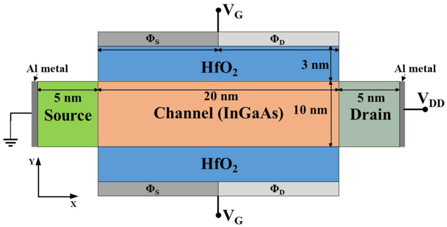
2. Device Structure
3. Computational Methods
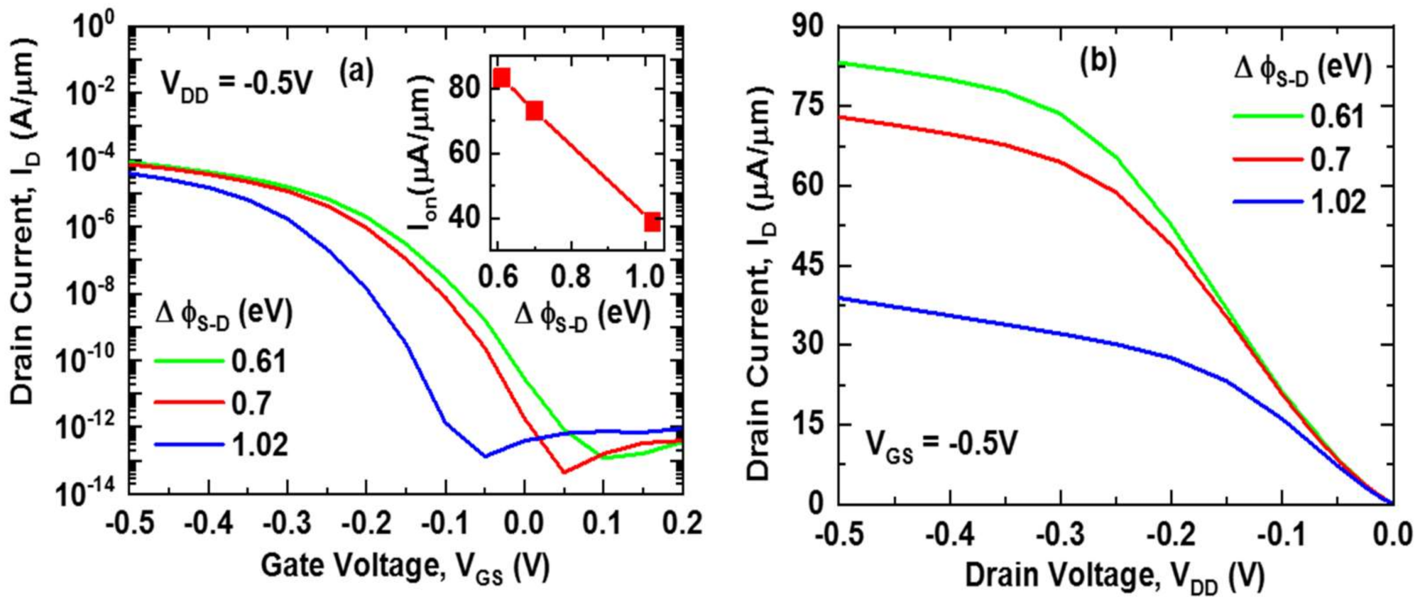
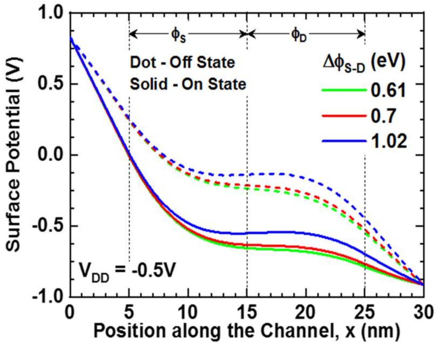
4. Results and Discussion
5. Performance Parameter Analysis
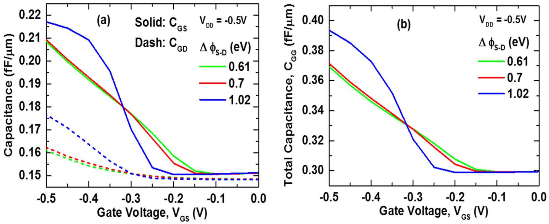
5.1. Capacitance Analysis
5.2. Digital Performance Parameters
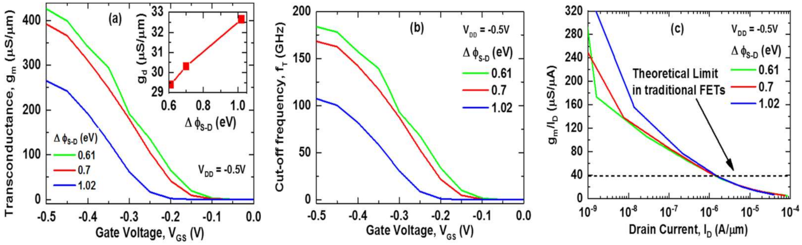
5.3. RF Performance Parameters
6. Conclusions
Author Contributions
Funding
Data Availability Statement
Conflicts of Interest
References
- Datta, S.; Bijesh, R.; Liu, H.; Mohata, D.; Narayanan, V. Tunnel transistors for energy efficient computing. IEEE Int. Reliab. Phys. Symp. 2013, 6A.3.1–6A.3.7. [Google Scholar] [CrossRef]
- Lu, H.; Seabaugh, A. Tunnel field-effect transistors: State-of-the-art. IEEE J. Electron Devices Soc. 2014, 2, 44–49. [Google Scholar] [CrossRef]
- Datta, S.; Liu, H.; Narayanan, V. Tunnel FET technology: A reliability perspective. Microelectron. Reliab. 2014, 54, 861–874. [Google Scholar] [CrossRef]
- Fischer, I.A.; Bakibillah, A.S.M.; Golve, M.; Hahnel, D.; Isemann, H.; Kottantharayil, A.; Oehme, M.; Schulze, J. Silicon tunneling field-effect transistors with tunneling in line with the gate field. IEEE Electron Device Lett. 2012, 34, 154–156. [Google Scholar] [CrossRef]
- Azam, S.M.T.; Bakibillah, A.S.M.; Kamal, M.A.S. Performance Evaluation of InGaAs Dielectric Engineered Tunnel Field-Effect Transistors. J. Nano Res. 2019, 59, 149–160. [Google Scholar] [CrossRef]
- Sedighi, B.; Hu, X.S.; Liu, H.; Nahas, J.J.; Niemier, M. Analog Circuit Design Using Tunnel-FETs. IEEE Trans. Circuits Syst. I Regul. Pap. 2014, 62, 39–48. [Google Scholar] [CrossRef]
- Biswas, A.; Luong, G.V.; Chowdhury, M.F.; Alper, C.; Zhao, Q.T.; Udrea, F.; Mantl, S.; Ionescu, A.M. Benchmarking of Homojunction Strained-Si NW Tunnel FETs for Basic Analog Functions. IEEE Trans. Electron Devices 2017, 64, 1441–1448. [Google Scholar] [CrossRef]
- Settino, F.; Lanuzza, M.; Strangio, S.; Crupi, F.; Palestri, P.; Esseni, D.; Selmi, L. Understanding the potential and limitations of tunnel FETs for low-voltage analog/mixed-signal circuits. IEEE Trans. Electron Devices 2017, 64, 2736. [Google Scholar] [CrossRef]
- Kim, Y.J.; Yoon, Y.J.; Seo, J.H.; Lee, S.M.; Cho, S.; Lee, J.H.; Kang, I.M. Effect of Ga fraction in InGaAs channel on performances of gate-all-around tunneling field-effect transistor. Semicond. Sci. Technol. 2014, 30, 015006. [Google Scholar] [CrossRef]
- Knoch, J.; Appenzeller, J. Modeling of high-performance p-type III-V heterojunction tunnel FETs. IEEE Electron Device Lett. 2010, 31, 305–307. [Google Scholar] [CrossRef]
- Verhulst, A.S.; Verreck, D.; Pourghaderi, M.A.; Van de Put, M.; Soree, B.; Groeseneken, G.; Collaert, N.; Thean, A.Y. Can p-channel tunnel field-effect transistors perform as good as n-channel? Appl. Phys. Lett. 2014, 105, 043103. [Google Scholar] [CrossRef]
- Verreck, D.; Verhulst, A.S.; Sorée, B.; Collaert, N.; Mocuta, A.; Thean, A.; Groeseneken, G. Improved source design for p-type tunnel field-effect transistors: Towards truly complementary logic. Appl. Phys. Lett. 2014, 105, 243506. [Google Scholar] [CrossRef]
- Huang, J.Z.; Long, P.; Povolotskyi, M.; Klimeck, G.; Rodwell, M.J. P-type tunnel FETs with triple heterojunctions. IEEE J. Electron Devices Soc. 2016, 4, 410–415. [Google Scholar] [CrossRef]
- Long, W.; Ou, H.; Kuo, J.M.; Chin, K.K. Dual-material gate (DMG) field effect transistor. IEEE Trans. Electron Devices 1999, 46, 865–870. [Google Scholar] [CrossRef]
- Orouji, A.A.; Arefinia, Z. Detailed simulation study of a dual material gate carbon nanotube field-effect transistor. Phys. E Low-Dimens. Syst. Nanostruct. 2009, 41, 552–557. [Google Scholar] [CrossRef]
- Djeffal, F.; Lakhdar, N.; Yousfi, A. An optimized design of 10-nm-scale dual-material surrounded gate MOSFETs for digital circuit applications. Phys. E Low-Dimens. Syst. Nanostruct. 2011, 44, 339–344. [Google Scholar] [CrossRef]
- Mehedi, I.M.; Alshareef, A.M.; Islam, M.R.; Hasan, M.T. GaN-based double-gate (DG) sub-10-nm MOSFETs: Effects of gate work function. J. Comput. Electron. 2018, 17, 663–669. [Google Scholar] [CrossRef]
- Chakraborty, S.; Mallik, A.; Sarkar, C.K. Subthreshold performance of dual-material gate CMOS devices and circuits for ultralow power analog/mixed-signal applications. IEEE Trans. Electron Devices 2008, 55, 827–832. [Google Scholar] [CrossRef]
- Kundu, A.; Koley, K.; Dutta, A.; Sarkar, C.K. Impact of gate metal work-function engineering for enhancement of subthreshold analog/RF performance of underlap dual material gate DG-FET. Microelectron. Reliab. 2014, 54, 2717–2722. [Google Scholar] [CrossRef]
- Saurabh, S.; Kumar, M.J. Novel attributes of a dual material gate nanoscale tunnel field-effect transistor. IEEE Trans. Electron Devices 2010, 58, 404–410. [Google Scholar] [CrossRef] [Green Version]
- Lv, Y.; Huang, Q.; Wang, H.; Chang, S.; He, J. A numerical study on graphene nanoribbon heterojunction dual-material gate tunnel FET. IEEE Electron Device Lett. 2016, 37, 1354–1357. [Google Scholar] [CrossRef]
- Noor, S.L.; Safa, S.; Khan, M.Z.R. Dual-material double-gate tunnel FET: Gate threshold voltage modeling and extraction. J. Comput. Electron. 2016, 15, 763–769. [Google Scholar] [CrossRef]
- Vishnoi, R.; Kumar, M.J. Compact analytical model of dual material gate tunneling field-effect transistor using interband tunneling and channel transport. IEEE Trans. Electron Devices 2014, 61, 2264–2270. [Google Scholar] [CrossRef]
- Zhang, A.; Mei, J.; Zhang, L.; He, H.; He, J.; Chan, M. Numerical study on dual material gate nanowire tunnel field-effect transistor. In Proceedings of the IEEE International Conference on Electron Devices and Solid-State Circuit (EDSSC), Bangkok, Thailand, 3–5 December 2012; pp. 1–5. [Google Scholar]
- SILVACO. ATLAS User’s Manual; SILVACO: Santa Clara, CA, USA, 2014. [Google Scholar]
- Rajamohanan, B.; Mohata, D.; Ali, A.; Datta, S. Insight into the output characteristics of III-V tunneling field effect transistors. Appl. Phys. Lett. 2013, 102, 092105. [Google Scholar] [CrossRef] [Green Version]
- Mookerjea, S.; Krishnan, R.; Datta, S.; Narayanan, V. On enhanced Miller capacitance effect in interband tunnel transistors. IEEE Electron Device Lett. 2009, 30, 1102–1104. [Google Scholar] [CrossRef]
- Zhang, Q.; Seabaugh, A. Can the interband tunnel FET outperform Si CMOS? In Proceedings of the IEEE Device Research Conference, Monterey, CA, USA, 15–19 September 2008; pp. 73–74. [Google Scholar]
- Kondekar, P.N.; Nigam, K.; Pandey, S.; Sharma, D. Design and Analysis of Polarity Controlled Electrically Doped Tunnel FET With Bandgap Engineering for Analog/RF Applications. IEEE Trans. Electron Devices 2016, 64, 412–418. [Google Scholar] [CrossRef]
- Sarkar, A.; Das, A.K.; De, S.; Sarkar, C.K. Effect of gate engineering in double-gate MOSFETs for analog/RF applications. Microelectron. J. 2012, 43, 873–882. [Google Scholar] [CrossRef]
- Madan, J.; Chaujar, R. Interfacial charge analysis of heterogeneous gate dielectric-gate all around-tunnel FET for improved device reliability. IEEE Trans. Device Mater. Reliab. 2016, 16, 227–234. [Google Scholar] [CrossRef]


| Source Side Electrode, ϕS (eV) | Drain Side Electrode, ϕD (eV) | Work Function Difference, ∆ϕS-D (eV) |
|---|---|---|
| Pt (5.65) | Ni (5.04) | 0.61 |
| Mo (4.95) | 0.70 | |
| W (4.63) | 1.02 |
| ∆ϕS-D (eV) | |||
|---|---|---|---|
| Parameters | 0.61 | 0.7 | 1.02 |
| τ (ps) | 2.22 | 2.55 | 5.07 |
| Pleak (µW/µm) | 7.09 × 10⁻⁴ | 4.53 × 10⁻⁵ | 9.77 × 10⁻⁶ |
| Pdyn (µW/µm) | 20.8 | 18.2 | 9.71 |
| Ptotal (µW/µm) | 20.8 | 18.2 | 9.71 |
| Eleak (aJ/µm) | 78.6 × 10⁻³ | 5.77 × 10⁻³ | 2.47 × 10⁻³ |
| Edyn (aJ/µm) | 46.2 | 46.4 | 49.2 |
| Etotal (aJ/µm) | 46.2 | 46.4 | 49.2 |
Publisher’s Note: MDPI stays neutral with regard to jurisdictional claims in published maps and institutional affiliations. |
© 2021 by the authors. Licensee MDPI, Basel, Switzerland. This article is an open access article distributed under the terms and conditions of the Creative Commons Attribution (CC BY) license (https://creativecommons.org/licenses/by/4.0/).
Share and Cite
Azam, S.M.T.; Bakibillah, A.S.M.; Hasan, M.T.; Kamal, M.A.S. Effect of Step Gate Work Function on InGaAs p-TFET for Low Power Switching Applications. Nanomaterials 2021, 11, 3166. https://doi.org/10.3390/nano11123166
Azam SMT, Bakibillah ASM, Hasan MT, Kamal MAS. Effect of Step Gate Work Function on InGaAs p-TFET for Low Power Switching Applications. Nanomaterials. 2021; 11(12):3166. https://doi.org/10.3390/nano11123166
Chicago/Turabian StyleAzam, Sayed Md Tariful, Abu Saleh Md Bakibillah, Md Tanvir Hasan, and Md Abdus Samad Kamal. 2021. "Effect of Step Gate Work Function on InGaAs p-TFET for Low Power Switching Applications" Nanomaterials 11, no. 12: 3166. https://doi.org/10.3390/nano11123166
APA StyleAzam, S. M. T., Bakibillah, A. S. M., Hasan, M. T., & Kamal, M. A. S. (2021). Effect of Step Gate Work Function on InGaAs p-TFET for Low Power Switching Applications. Nanomaterials, 11(12), 3166. https://doi.org/10.3390/nano11123166