
Modal Properties of Photonic Crystal Cavities and Applications to Lasers

 , , , , and
Abstract
:1. Introduction
1.1. Key Mode Characteristics: The Q-Factor and the Mode Volume
1.2. The Structure of This Paper
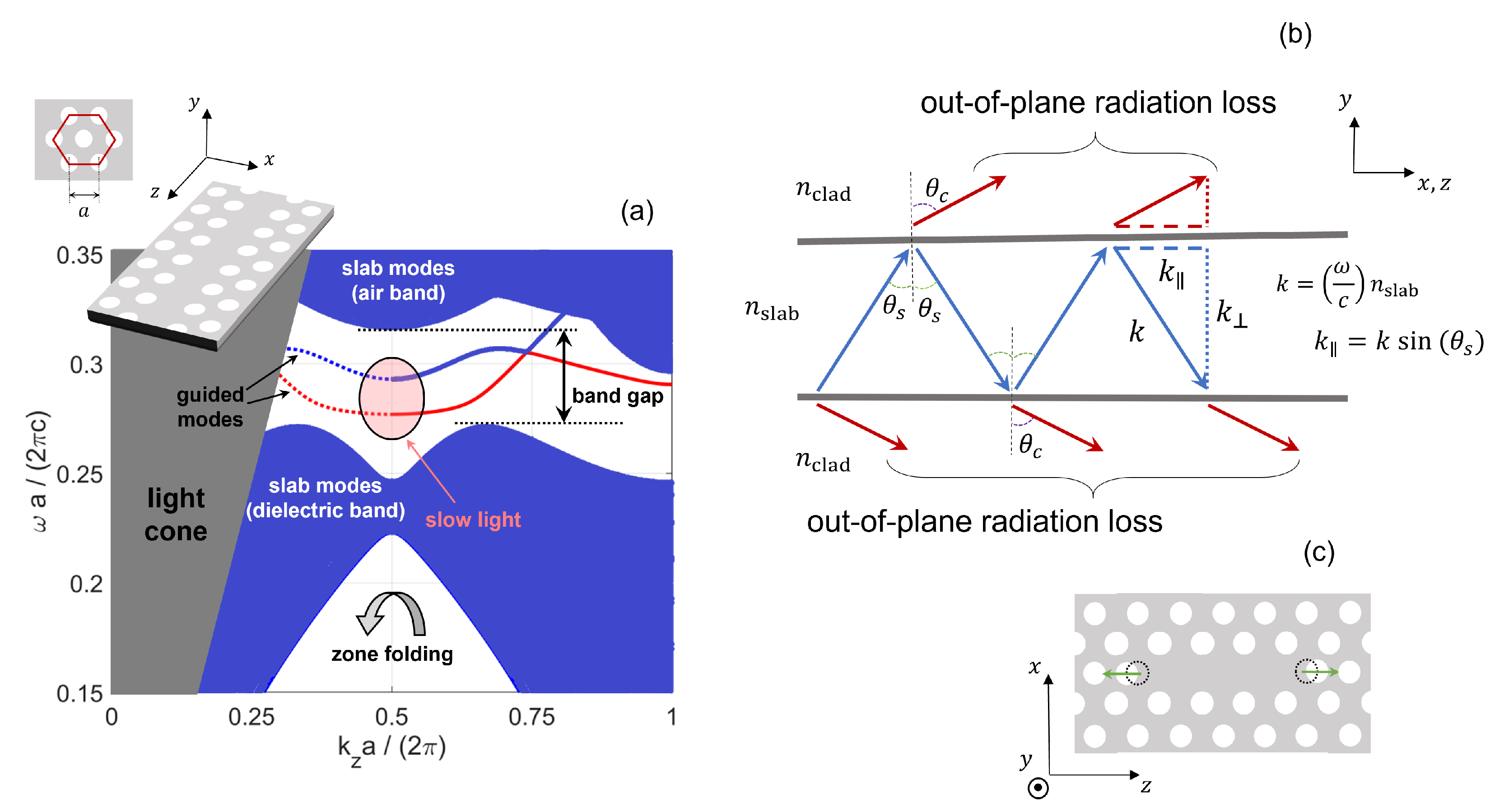
2. Fundamental Principles of Light Confinement in Photonic Crystal Structures
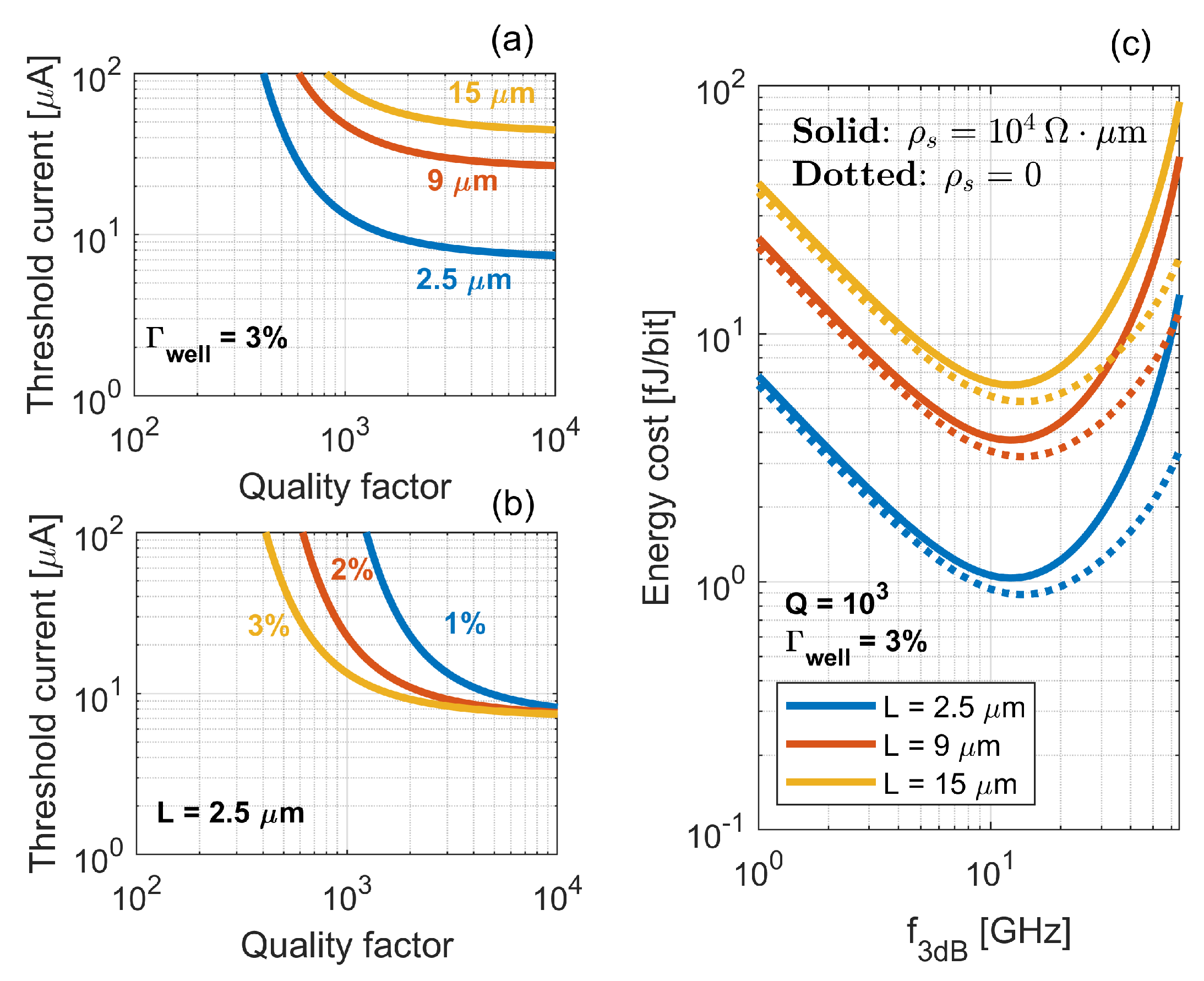
3. Microcavity Lasers for Energy-Efficient Communications
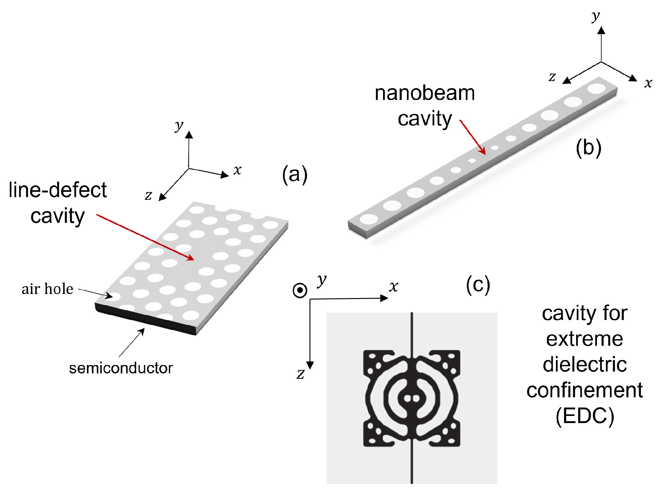
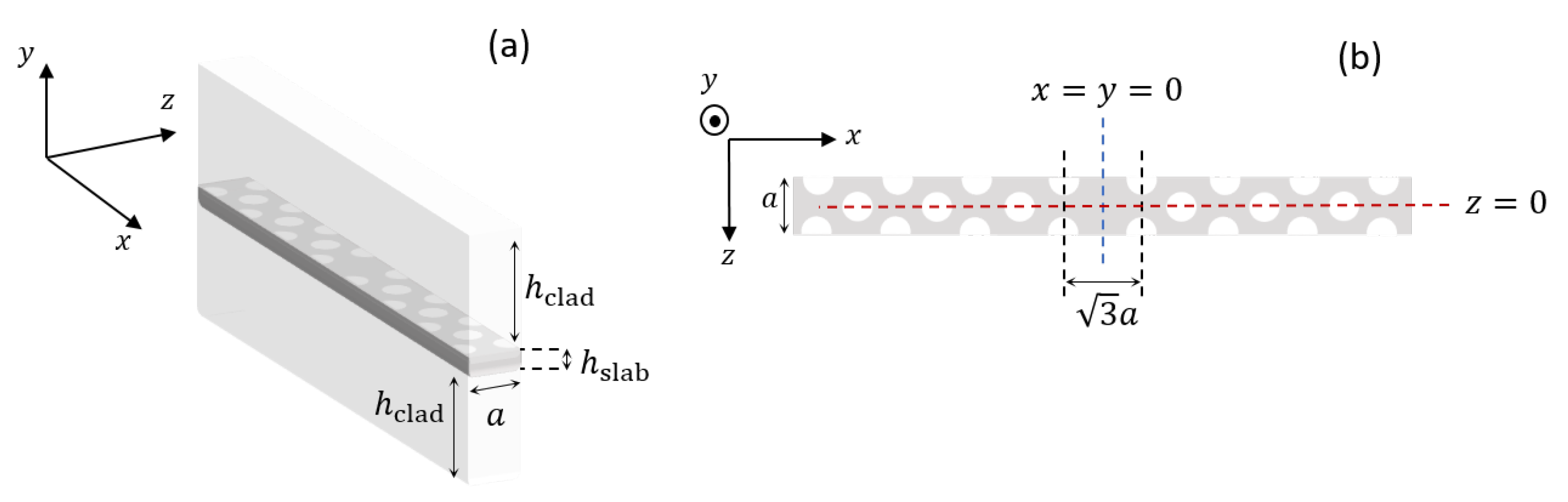
4. Line-Defect Cavities
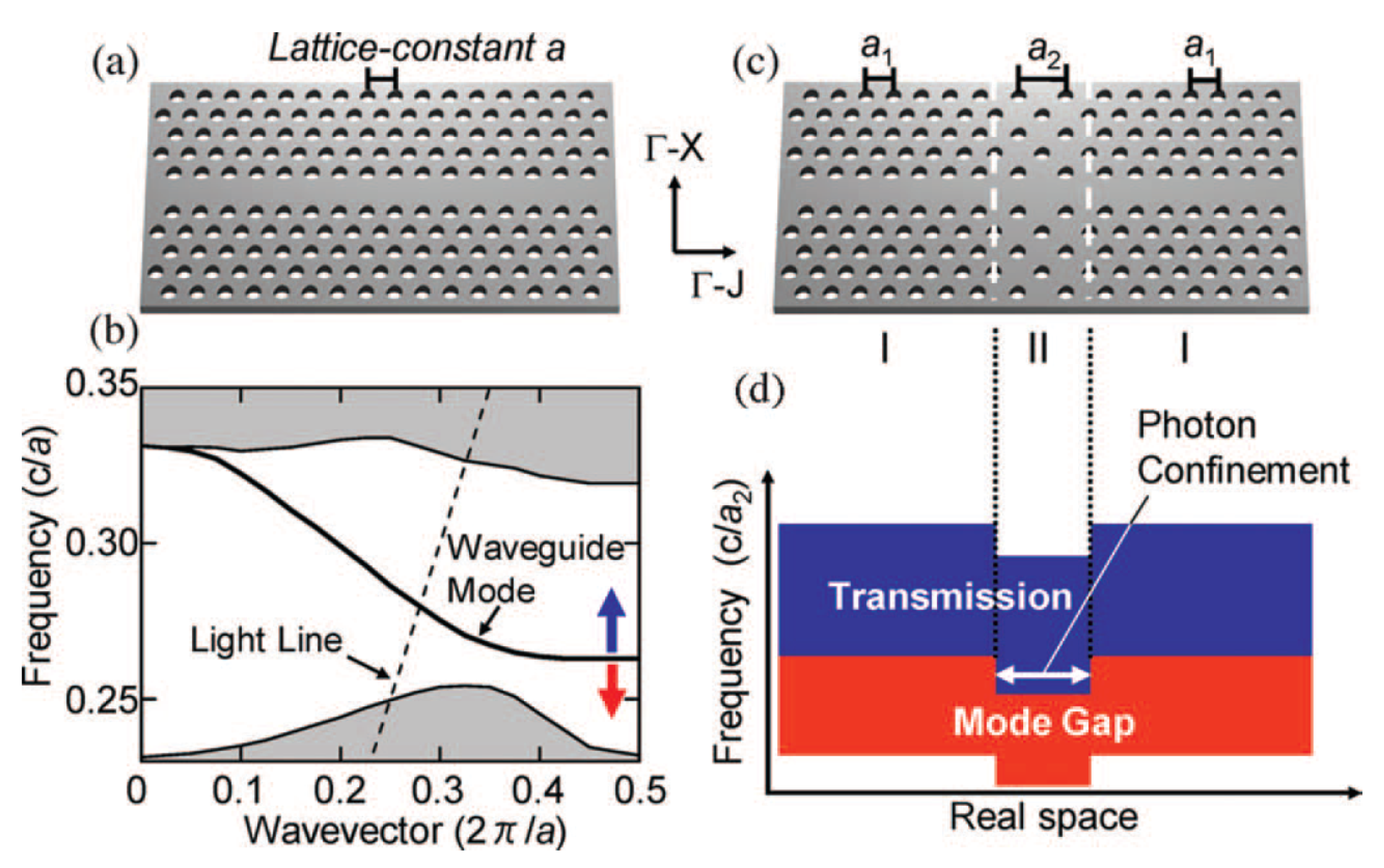
4.1. Dispersion Relation
4.2. Bloch Modes
4.3. Resonance Condition
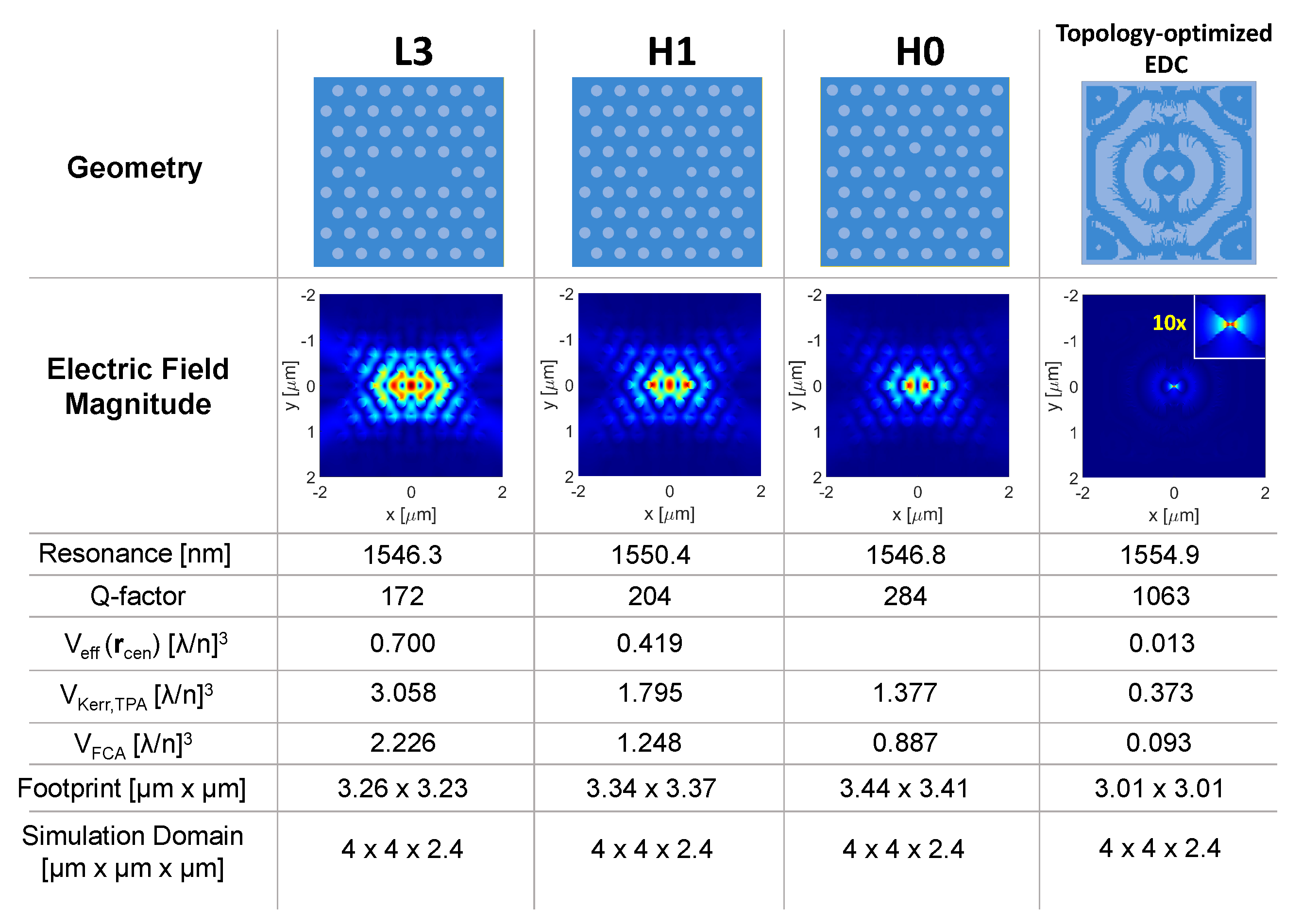
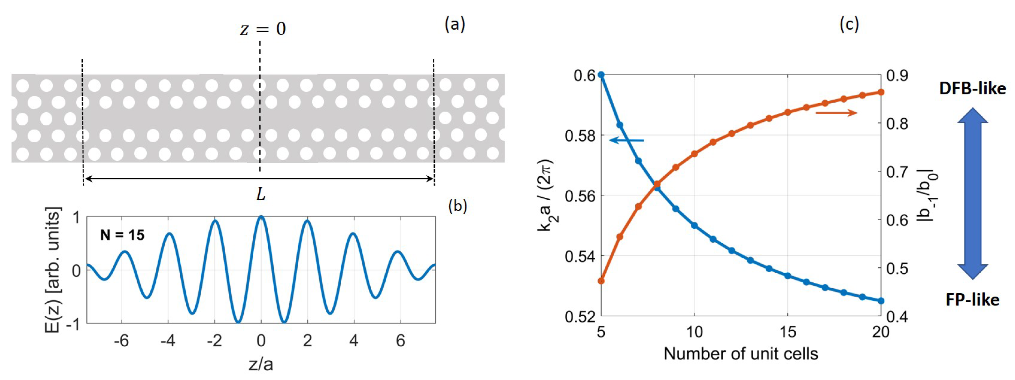
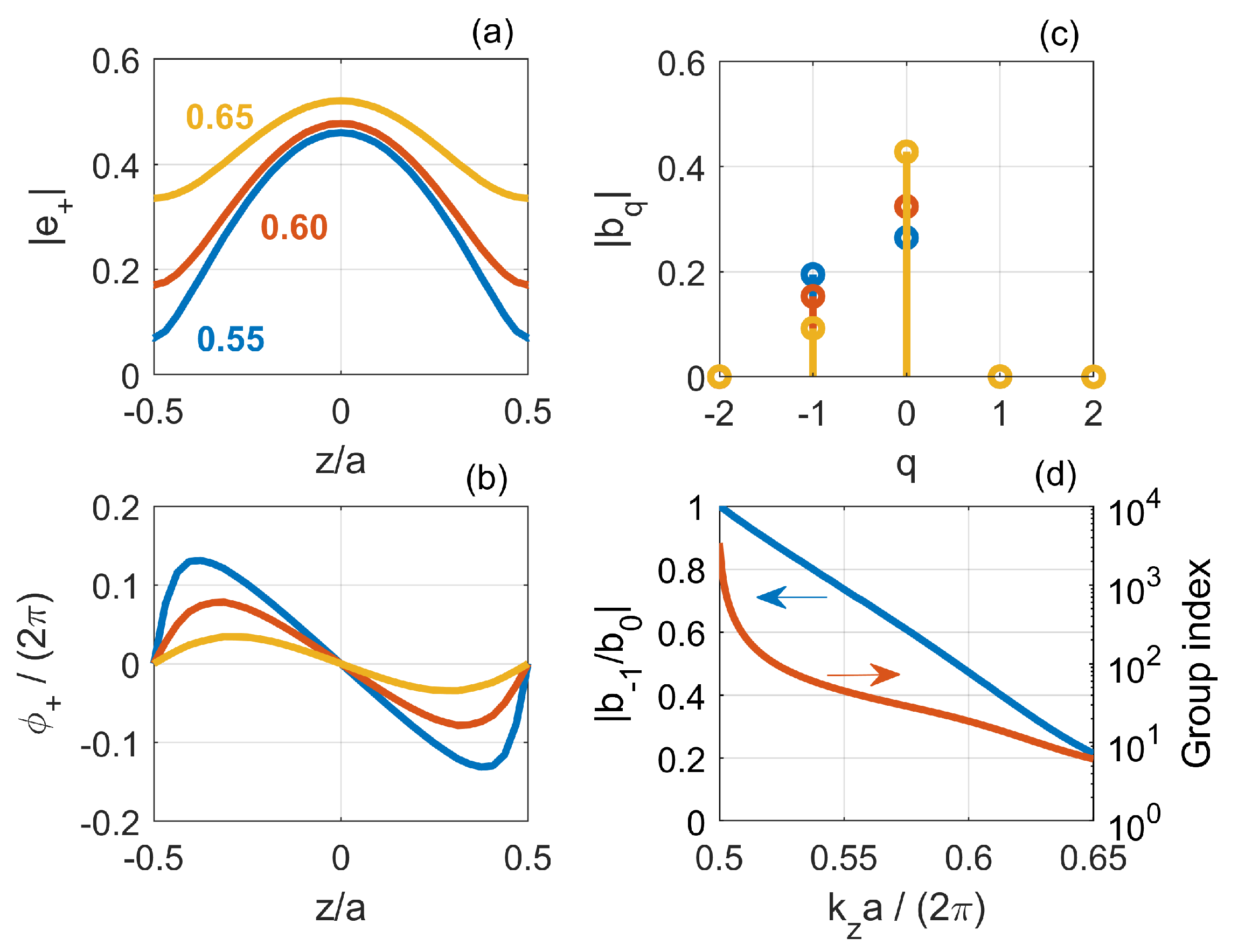
4.4. Resonant Modes: Real Space Distribution
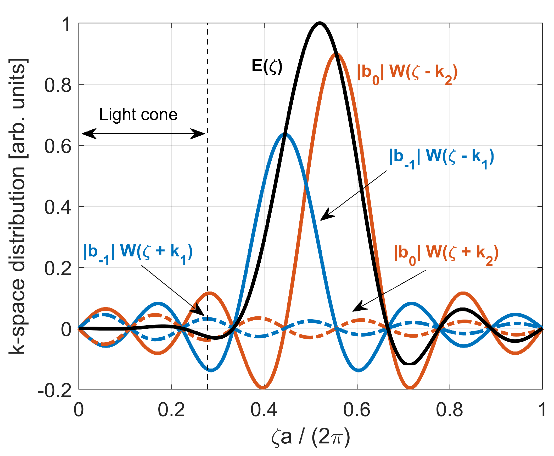
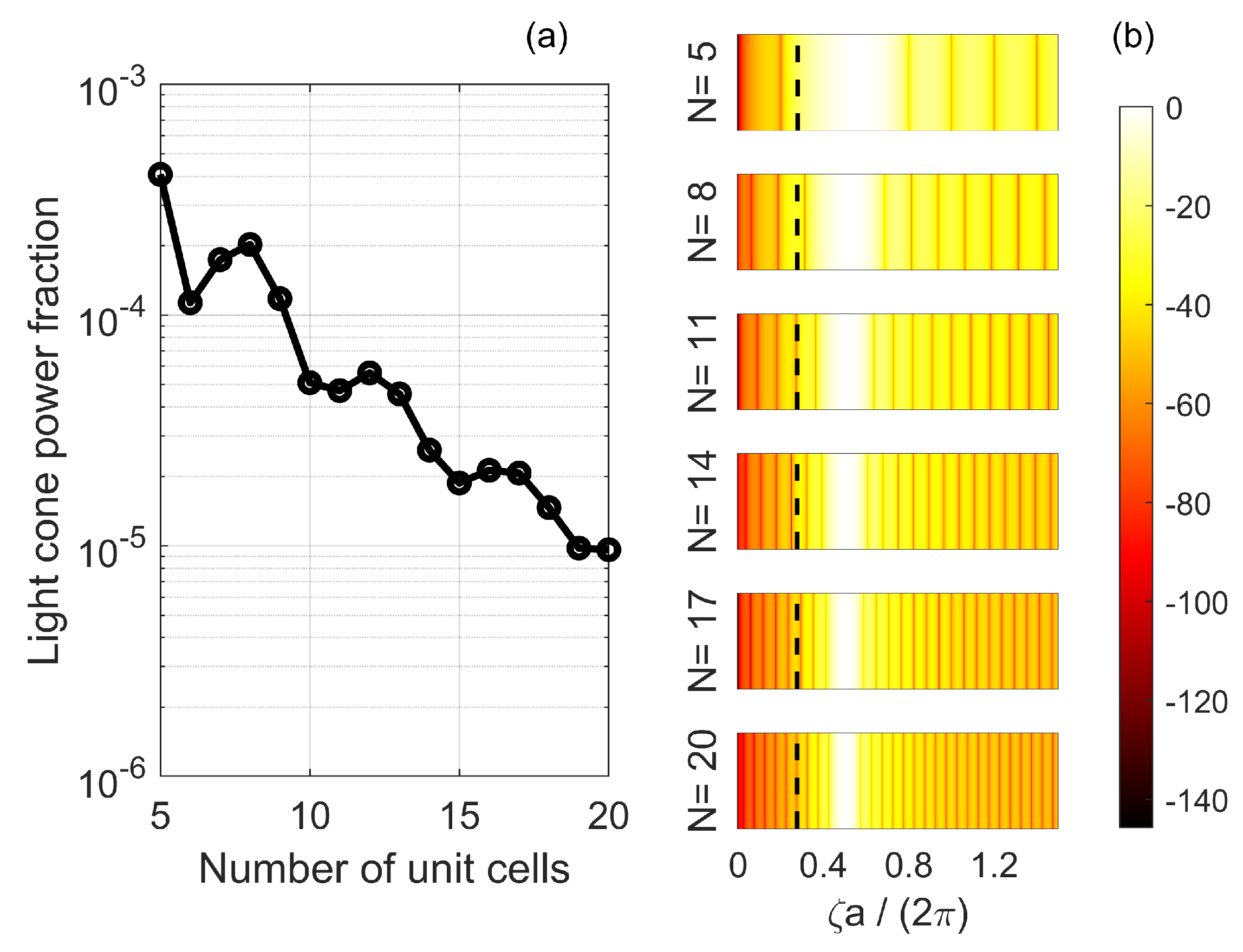
4.5. Resonant Modes: Reciprocal Space Distribution and Radiation Loss
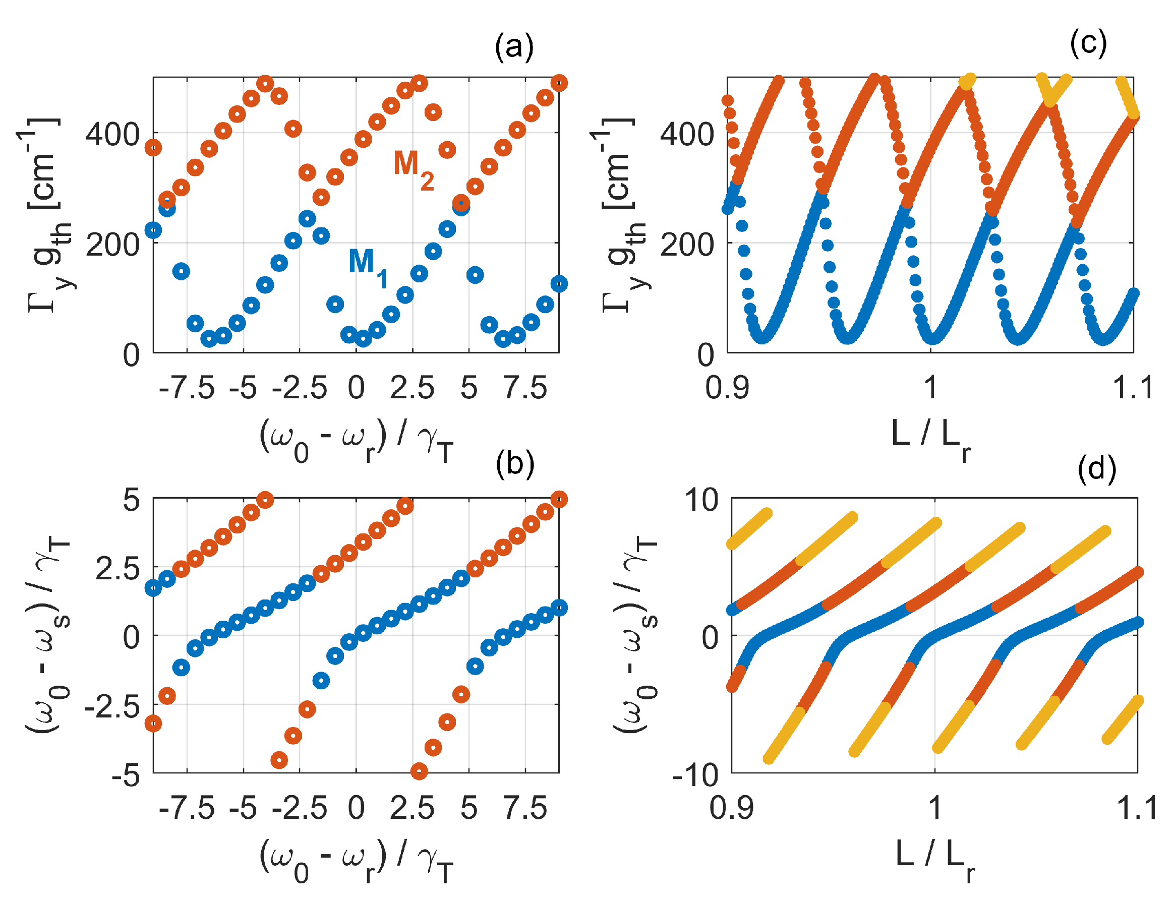
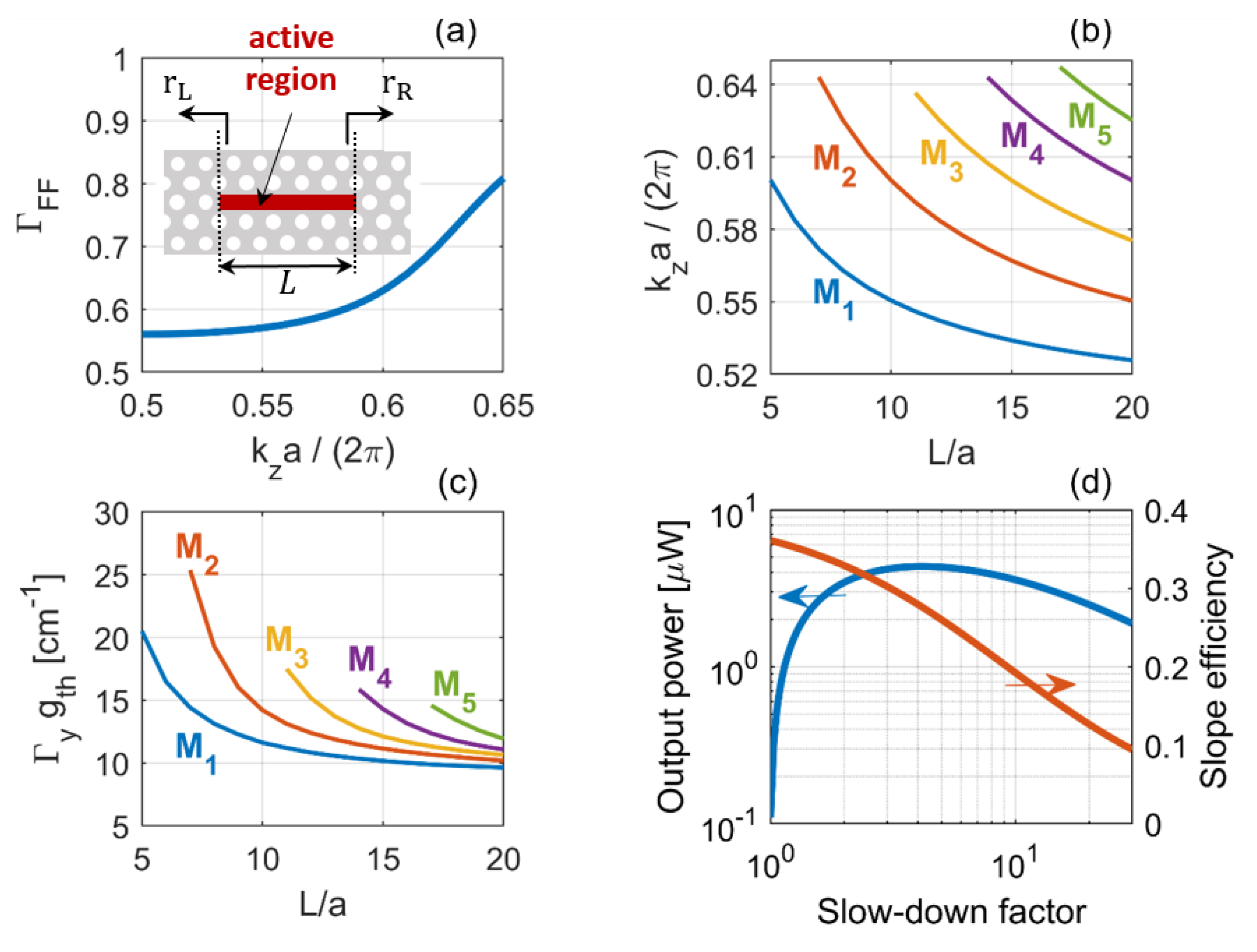
4.6. Slow-Light Photonic Crystal Lasers
5. Fano Laser
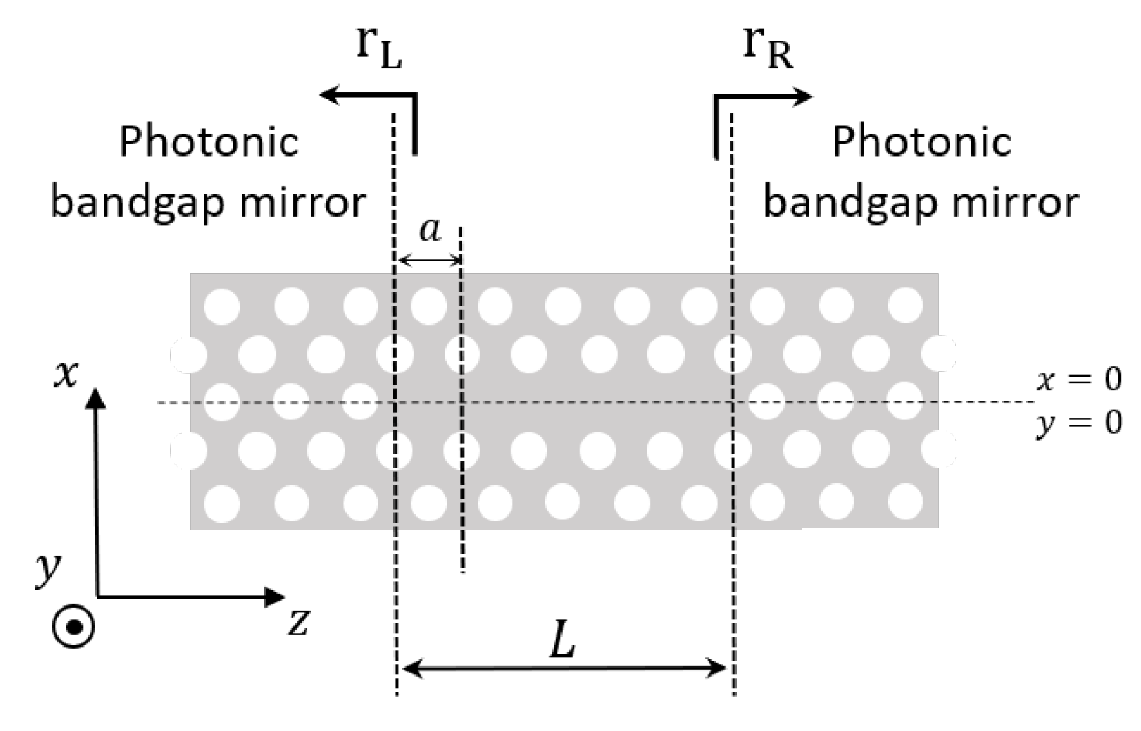
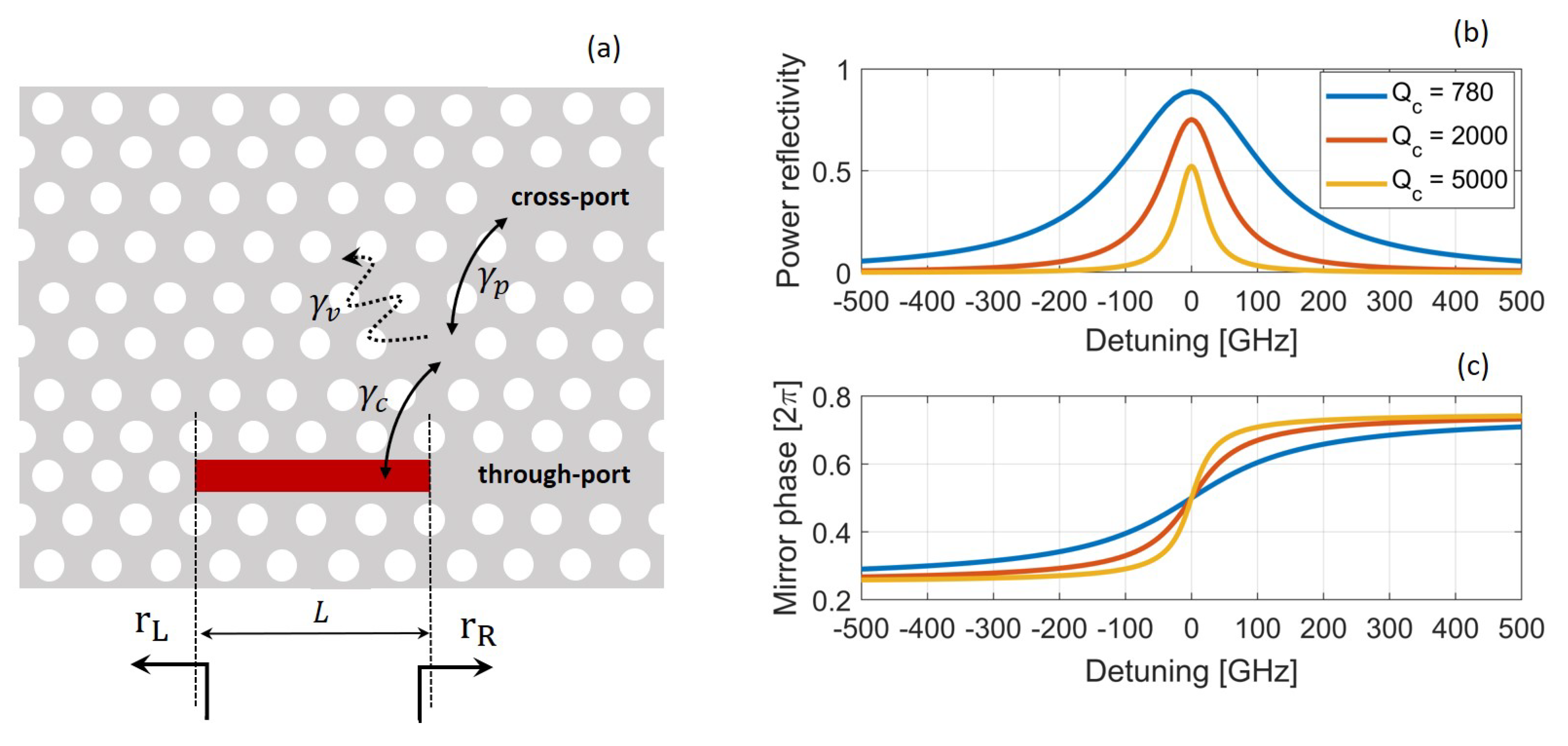
5.1. Fano Mirror
5.2. Tuning Characteristics
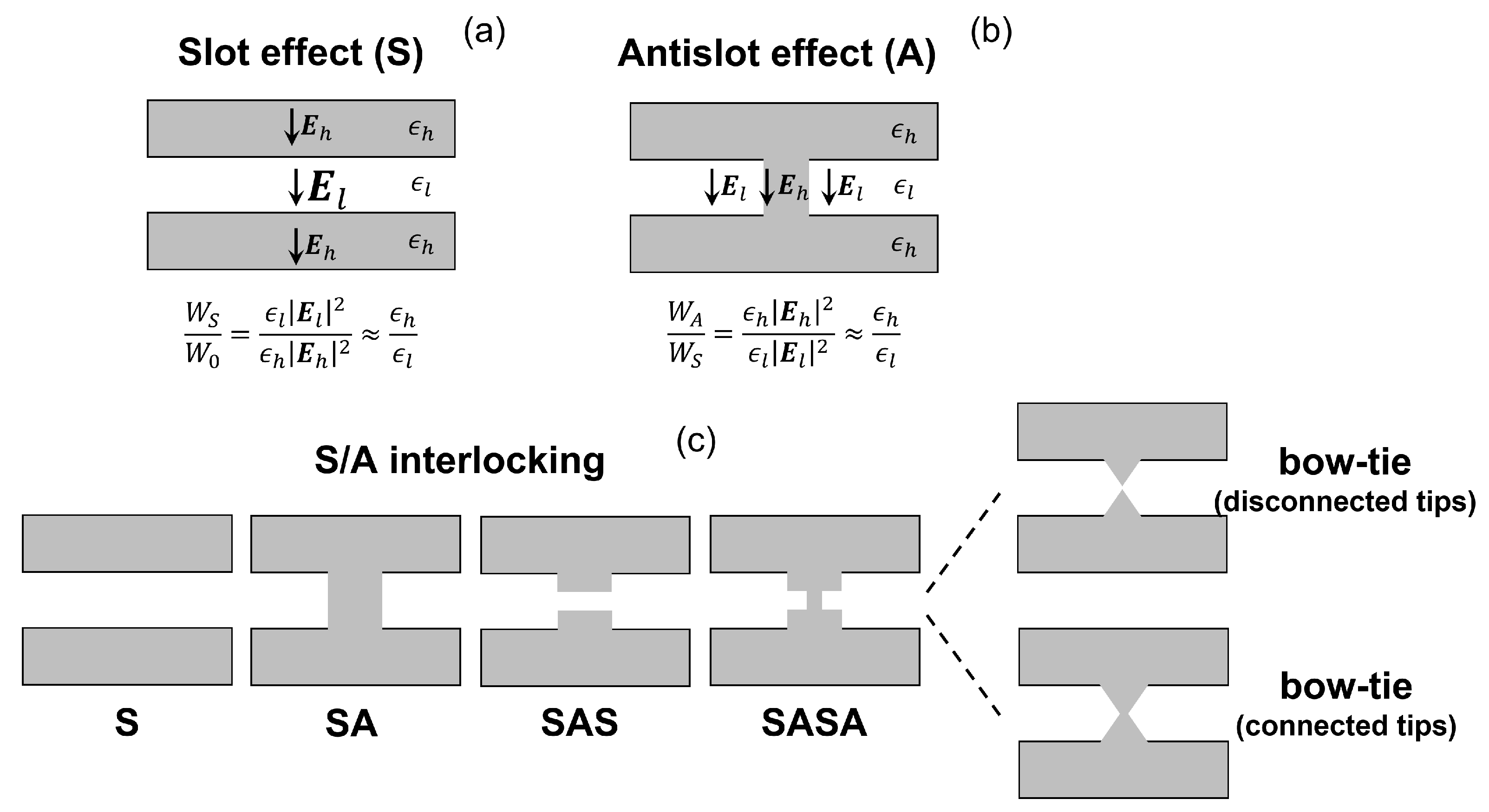
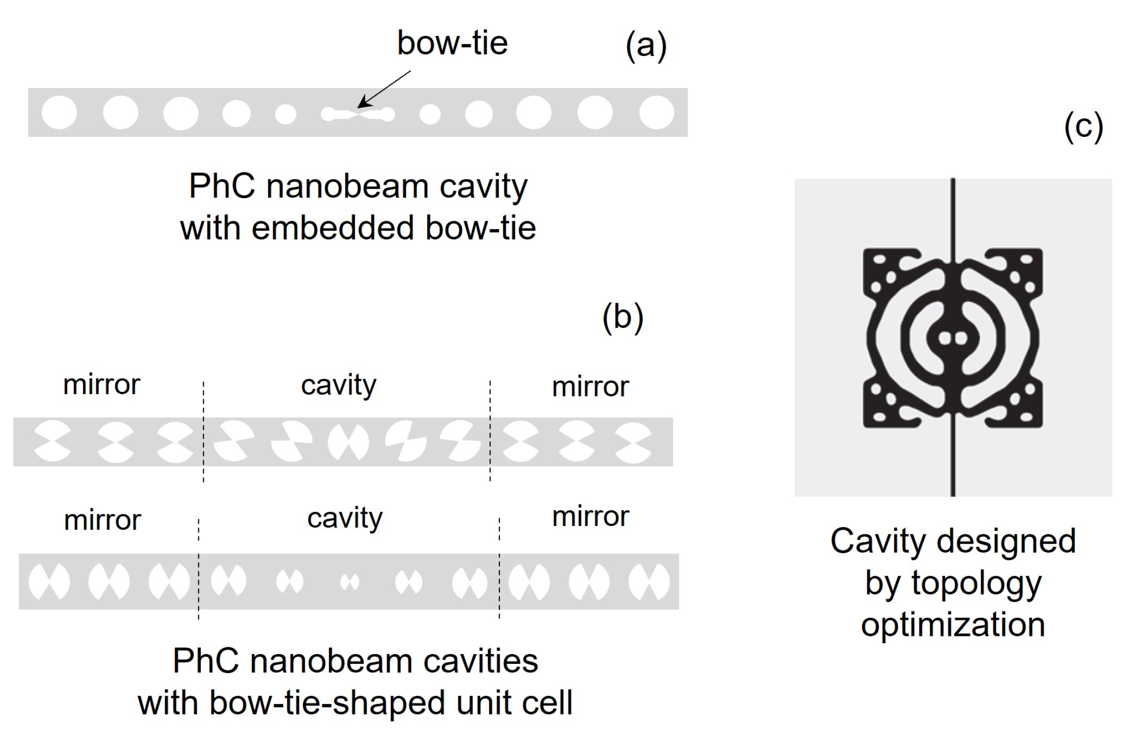
6. EDC Cavities
7. Conclusions
Funding
Data Availability Statement
Acknowledgments
Conflicts of Interest
References
- Joannopoulos, J.D.; Johnson, S.G.; Winn, J.N.; Meade, R.D. Photonic Crystals: Molding the Flow of Light, 2nd ed.; Princeton University Press: Princeton, NJ, USA, 2008. [Google Scholar]
- Ashcroft, N.W.; Mermin, N.D. Solid State Physics; Brooks/Cole: Boston, MA, USA, 1976. [Google Scholar]
- Painter, O.; Lee, R.K.; Scherer, A.; Yariv, A.; O’Brien, J.D.; Dapkus, P.D.; Kim, I. Two-Dimensional Photonic Band-Gap Defect Mode Laser. Science 1999, 284, 1819–1821. [Google Scholar] [CrossRef] [Green Version]
- Park, H.G.; Kim, S.H.; Kwon, S.H.; Ju, Y.G.; Yang, J.K.; Baek, J.H.; Kim, S.B.; Lee, Y.H. Electrically Driven Single-Cell Photonic Crystal Laser. Science 2004, 305, 1444–1447. [Google Scholar] [CrossRef]
- Ellis, B.; Mayer, M.A.; Shambat, G.; Sarmiento, T.; Harris, J.; Haller, E.E.; Vučković, J. Ultralow-threshold electrically pumped quantum-dot photonic-crystal nanocavity laser. Nat. Photonics 2011, 5, 297–300. [Google Scholar] [CrossRef]
- Zhou, T.; Tang, M.; Xiang, G.; Xiang, B.; Hark, S.; Martin, M.; Baron, T.; Pan, S.; Park, J.S.; Liu, Z.; et al. Continuous-wave quantum dot photonic crystal lasers grown on on-axis Si (001). Nat. Commun. 2020, 11, 977. [Google Scholar] [CrossRef] [Green Version]
- Quan, Q.; Loncar, M. Deterministic design of wavelength scale, ultra-high Q photonic crystal nanobeam cavities. Opt. Express 2011, 19, 18529–18542. [Google Scholar] [CrossRef] [Green Version]
- Hu, S.; Weiss, S.M. Design of Photonic Crystal Cavities for Extreme Light Concentration. ACS Photonics 2016, 3, 1647–1653. [Google Scholar] [CrossRef]
- Choi, H.; Heuck, M.; Englund, D. Self-Similar Nanocavity Design with Ultrasmall Mode Volume for Single-Photon Nonlinearities. Phys. Rev. Lett. 2017, 118, 223605. [Google Scholar] [CrossRef] [PubMed] [Green Version]
- Wang, F.; Christiansen, R.E.; Yu, Y.; Mørk, J.; Sigmund, O. Maximizing the quality factor to mode volume ratio for ultra-small photonic crystal cavities. Appl. Phys. Lett. 2018, 113, 241101. [Google Scholar] [CrossRef]
- Jackson, J.D. Classical Electrodynamics, 3rd ed.; John Wiley & Sons, Inc.: Hoboken, NJ, USA, 1999. [Google Scholar]
- Asano, T.; Song, B.; Akahane, Y.; Noda, S. Ultrahigh-Q Nanocavities in Two-Dimensional Photonic Crystal Slabs. IEEE J. Sel. Top. Quantum Electron. 2006, 12, 1123–1134. [Google Scholar] [CrossRef]
- Coccioli, R.; Boroditsky, M.; Kim, K.; Rahmat-Samii, Y.; Yablonovitch, E. Smallest possible electromagnetic mode volume in a dielectric cavity. IEE Proc. Optoelectron. 1998, 145, 391–397. [Google Scholar] [CrossRef]
- Mørk, J.; Lippi, G.L. Rate equation description of quantum noise in nanolasers with few emitters. Appl. Phys. Lett. 2018, 112, 141103. [Google Scholar] [CrossRef]
- Purcell, E.M. Spontaneous Emission Probabilities at Radio Frequencies. Phys. Rev. 1946, 69, 681. [Google Scholar] [CrossRef]
- Kristensen, P.T.; Herrmann, K.; Intravaia, F.; Busch, K. Modeling electromagnetic resonators using quasinormal modes. Adv. Opt. Photon. 2020, 12, 612–708. [Google Scholar] [CrossRef] [Green Version]
- Kristensen, P.T.; Vlack, C.V.; Hughes, S. Generalized effective mode volume for leaky optical cavities. Opt. Lett. 2012, 37, 1649–1651. [Google Scholar] [CrossRef]
- Kristensen, P.T.; Hughes, S. Modes and Mode Volumes of Leaky Optical Cavities and Plasmonic Nanoresonators. ACS Photonics 2014, 1, 2–10. [Google Scholar] [CrossRef] [Green Version]
- Akahane, Y.; Asano, T.; Song, B.S.; Noda, S. Fine-tuned high-Q photonic-crystal nanocavity. Opt. Express 2005, 13, 1202–1214. [Google Scholar] [CrossRef]
- Barclay, P.E.; Srinivasan, K.; Painter, O. Nonlinear response of silicon photonic crystal microresonators excited via an integrated waveguide and fiber taper. Opt. Express 2005, 13, 801–820. [Google Scholar] [CrossRef] [Green Version]
- Johnson, T.J.; Borselli, M.; Painter, O. Self-induced optical modulation of the transmission through a high-Q silicon microdisk resonator. Opt. Express 2006, 14, 817–831. [Google Scholar] [CrossRef] [PubMed]
- Notomi, M. Manipulating light with strongly modulated photonic crystals. Rep. Prog. Phys. 2010, 73, 096501. [Google Scholar] [CrossRef]
- Coldren, L.A.; Corzine, S.W.; Mašanović, M. Diode Lasers and Photonic Integrated Circuits, 2nd ed.; John Wiley & Sons, Inc.: Hoboken, NJ, USA, 2012. [Google Scholar]
- Ghione, G. Semiconductor Devices for High-Speed Optoelectronics; Cambridge University Press: Cambridge, MA, USA, 2009. [Google Scholar] [CrossRef] [Green Version]
- Blood, P. On the dimensionality of optical absorption, gain, and recombination in quantum-confined structures. IEEE J. Quantum Electron. 2000, 36, 354–362. [Google Scholar] [CrossRef]
- Sato, T.; Takeda, K.; Shinya, A.; Notomi, M.; Hasebe, K.; Kakitsuka, T.; Matsuo, S. Photonic Crystal Lasers for Chip-to-Chip and On-Chip Optical Interconnects. IEEE J. Sel. Top. Quantum Electron. 2015, 21, 728–737. [Google Scholar] [CrossRef]
- Soljačić, M.; Joannopoulos, J.D. Enhancement of nonlinear effects using photonic crystals. Nat. Mater. 2005, 3, 211–219. [Google Scholar] [CrossRef]
- Notomi, M.; Nozaki, K.; Shinya, A.; Matsuo, S.; Kuramochi, E. Toward fJ/bit optical communication in a chip. Opt. Commun. 2014, 314, 3–17. [Google Scholar] [CrossRef] [Green Version]
- Nozaki, K.; Tanabe, T.; Shinya, A.; Matsuo, S.; Sato, T.; Taniyama, H.; Notomi, M. Sub-femtojoule all-optical switching using a photonic-crystal nanocavity. Nat. Photonics 2010, 4, 477–483. [Google Scholar] [CrossRef]
- Nozaki, K.; Shinya, A.; Matsuo, S.; Suzaki, Y.; Segawa, T.; Sato, T.; Kawaguchi, Y.; Takahashi, R.; Notomi, M. Ultralow-power all-optical RAM based on nanocavities. Nat. Photonics 2012, 6, 248–252. [Google Scholar] [CrossRef]
- Kuramochi, E.; Nozaki, K.; Shinya, A.; Takeda, K.; Sato, T.; Matsuo, S.; Taniyama, H.; Sumikura, H.; Notomi, M. Large-scale integration of wavelength-addressable all-optical memories on a photonic crystal chip. Nat. Photonics 2014, 8, 474–481. [Google Scholar] [CrossRef]
- Pitruzzello, G.; Krauss, T.F. Photonic crystal resonances for sensing and imaging. J. Opt. 2018, 20, 073004. [Google Scholar] [CrossRef]
- Tanabe, T.; Sumikura, H.; Taniyama, H.; Shinya, A.; Notomi, M. All-silicon sub-Gb/s telecom detector with low dark current and high quantum efficiency on chip. Appl. Phys. Lett. 2010, 96, 101103. [Google Scholar] [CrossRef] [Green Version]
- Noda, S.; Fujita, M.; Asano, T. Spontaneous-emission control by photonic crystals and nanocavities. Nat. Photonics 2007, 1, 449–458. [Google Scholar] [CrossRef]
- Tiecke, T.G.; Thompson, J.D.; de Leon, N.P.; Liu, L.R.; Vuletić, V.; Lukin, M.D. Nanophotonic quantum phase switch with a single atom. Nature 2014, 508, 241–244. [Google Scholar] [CrossRef] [Green Version]
- Preble, S.F.; Xu, Q.; Lipson, M. Changing the colour of light in a silicon resonator. Nat. Photonics 2007, 1, 293–296. [Google Scholar] [CrossRef]
- Tanabe, T.; Notomi, M.; Taniyama, H.; Kuramochi, E. Dynamic Release of Trapped Light from an Ultrahigh-Q Nanocavity via Adiabatic Frequency Tuning. Phys. Rev. Lett. 2009, 102, 043907. [Google Scholar] [CrossRef] [Green Version]
- Raineri, F.; Bazin, A.; Raj, R. Optically Pumped Semiconductor Photonic Crystal Lasers. In Compact Semiconductor Lasers; John Wiley & Sons, Ltd.: Hoboken, NJ, USA, 2014; Chapter 2; pp. 33–90. [Google Scholar] [CrossRef]
- Fitsios, D.; Raineri, F. Chapter Five—Photonic Crystal Lasers and Nanolasers on Silicon. In Silicon Photonics; Lourdudoss, S., Chen, R.T., Jagadish, C., Eds.; Elsevier: Amsterdam, The Netherlands, 2018; Volume 99, pp. 97–137. [Google Scholar] [CrossRef]
- Mørk, J.; Yu, Y.; Rasmussen, T.S.; Semenova, E.; Yvind, K. Semiconductor Fano Lasers. IEEE J. Sel. Top. Quantum Electron. 2019, 25, 1–14. [Google Scholar] [CrossRef] [Green Version]
- Sze, S.M.; Ng, K.K. Physics of Semiconductor Devices; John Wiley & Sons, Ltd.: Hoboken, NJ, USA, 2006. [Google Scholar]
- Yablonovitch, E.; Gmitter, T.J.; Meade, R.D.; Rappe, A.M.; Brommer, K.D.; Joannopoulos, J.D. Donor and acceptor modes in photonic band structure. Phys. Rev. Lett. 1991, 67, 3380–3383. [Google Scholar] [CrossRef]
- Johnson, S.G.; Joannopoulos, J.D. Block-iterative frequency-domain methods for Maxwell’s equations in a planewave basis. Opt. Express 2001, 8, 173–190. [Google Scholar] [CrossRef] [Green Version]
- Melati, D.; Melloni, A.; Morichetti, F. Real photonic waveguides: Guiding light through imperfections. Adv. Opt. Photon. 2014, 6, 156–224. [Google Scholar] [CrossRef] [Green Version]
- Krauss, T.F. Slow light in photonic crystal waveguides. J. Phys. D Appl. Phys. 2007, 40, 2666–2670. [Google Scholar] [CrossRef] [Green Version]
- Baba, T. Slow light in photonic crystals. Nat. Photonics 2008, 2. [Google Scholar] [CrossRef]
- Okano, M.; Yamada, T.; Sugisaka, J.; Yamamoto, N.; Itoh, M.; Sugaya, T.; Komori, K.; Mori, M. Analysis of two-dimensional photonic crystal L-type cavities with low-refractive-index material cladding. J. Opt. 2010, 12, 075101. [Google Scholar] [CrossRef]
- Vučković, J.; Loncar, M.; Mabuchi, H.; Scherer, A. Optimization of the Q factor in photonic crystal microcavities. IEEE J. Quantum Electron. 2002, 38, 850–856. [Google Scholar] [CrossRef] [Green Version]
- Akahane, Y.; Asano, T.; Song, B.S.; Noda, S. High-Q photonic nanocavity in a two-dimensional photonic crystal. Nature 2003, 425, 944–947. [Google Scholar] [CrossRef]
- Kuramochi, E.; Duprez, H.; Kim, J.; Takiguchi, M.; Takeda, K.; Fujii, T.; Nozaki, K.; Shinya, A.; Sumikura, H.; Taniyama, H.; et al. Room temperature continuous-wave nanolaser diode utilized by ultrahigh-Q few-cell photonic crystal nanocavities. Opt. Express 2018, 26, 26598–26617. [Google Scholar] [CrossRef]
- Zhang, Z.; Qiu, M. Small-volume waveguide-section high Q microcavities in 2D photonic crystal slabs. Opt. Express 2004, 12, 3988–3995. [Google Scholar] [CrossRef]
- Song, B.S.; Noda, S.; Asano, T.; Akahane, Y. Ultra-high-Q photonic double-heterostructure nanocavity. Nat. Mater. 2005, 4, 207–210. [Google Scholar] [CrossRef]
- Sauvan, C.; Hugonin, J.P.; Lalanne, P. Difference between penetration and damping lengths in photonic crystal mirrors. Appl. Phys. Lett. 2009, 95, 211101. [Google Scholar] [CrossRef] [Green Version]
- Takeda, K.; Sato, T.; Shinya, A.; Nozaki, K.; Kobayashi, W.; Taniyama, H.; Notomi, M.; Hasebe, K.; Kakitsuka, T.; Matsuo, S. Few-fJ/bit data transmissions using directly modulated lambda-scale embedded active region photonic-crystal lasers. Nat. Photonics 2013, 7, 569–575. [Google Scholar] [CrossRef]
- Tanaka, Y.; Asano, T.; Noda, S. Design of Photonic Crystal Nanocavity with Q-Factor of ∼109. J. Light. Technol. 2008, 26, 1532–1539. [Google Scholar] [CrossRef] [Green Version]
- Asano, T.; Ochi, Y.; Takahashi, Y.; Kishimoto, K.; Noda, S. Photonic crystal nanocavity with a Q factor exceeding eleven million. Opt. Express 2017, 25, 1769–1777. [Google Scholar] [CrossRef]
- Notomi, M.; Taniyama, H. On-demand ultrahigh-Q cavity formation and photon pinning via dynamic waveguide tuning. Opt. Express 2008, 16, 18657–18666. [Google Scholar] [CrossRef]
- Halioua, Y.; Bazin, A.; Monnier, P.; Karle, T.J.; Roelkens, G.; Sagnes, I.; Raj, R.; Raineri, F. Hybrid III-V semiconductor/silicon nanolaser. Opt. Express 2011, 19, 9221–9231. [Google Scholar] [CrossRef] [Green Version]
- Jeong, K.Y.; No, Y.S.; Hwang, Y.; Kim, K.S.; Seo, M.K.; Park, H.G.; Lee, Y.H. Electrically driven nanobeam laser. Nat. Commun. 2013, 4, 2822. [Google Scholar] [CrossRef] [Green Version]
- Crosnier, G.; Sanchez, D.; Bouchoule, S.; Monnier, P.; Beaudoin, G.; Sagnes, I.; Raj, R.; Raineri, F. Hybrid indium phosphide-on-silicon nanolaser diode. Nat. Photonics 2017, 11, 297–300. [Google Scholar] [CrossRef]
- Albrechtsen, M.; Lahijani, B.V.; Christiansen, R.E.; Nguyen, V.T.H.; Casses, L.N.; Hansen, S.E.; Stenger, N.; Sigmund, O.; Jansen, H.; Mørk, J.; et al. Nanometer-scale photon confinement inside dielectrics. arXiv 2021, arXiv:2108.01681. [Google Scholar]
- Ning, C.Z. Semiconductor nanolasers and the size-energy-efficiency challenge: A review. Adv. Photonics 2019, 1, 1–10. [Google Scholar] [CrossRef]
- Takeda, K.; Tsurugaya, T.; Fujii, T.; Shinya, A.; Maeda, Y.; Tsuchizawa, T.; Nishi, H.; Notomi, M.; Kakitsuka, T.; Matsuo, S. Optical links on silicon photonic chips using ultralow-power consumption photonic-crystal lasers. Opt. Express 2021, 29, 26082–26092. [Google Scholar] [CrossRef]
- Takiguchi, M.; Taniyama, H.; Sumikura, H.; Birowosuto, M.D.; Kuramochi, E.; Shinya, A.; Sato, T.; Takeda, K.; Matsuo, S.; Notomi, M. Systematic study of thresholdless oscillation in high-β buried multiple-quantum-well photonic crystal nanocavity lasers. Opt. Express 2016, 24, 3441–3450. [Google Scholar] [CrossRef]
- Ota, Y.; Kakuda, M.; Watanabe, K.; Iwamoto, S.; Arakawa, Y. Thresholdless quantum dot nanolaser. Opt. Express 2017, 25, 19981–19994. [Google Scholar] [CrossRef]
- Khurgin, J.B.; Noginov, M.A. How Do the Purcell Factor, the Q-Factor, and the Beta Factor Affect the Laser Threshold? Laser Photonics Rev. 2021, 15, 2000250. [Google Scholar] [CrossRef]
- Matsuo, S.; Kakitsuka, T. Low-operating-energy directly modulated lasers for short-distance optical interconnects. Adv. Opt. Photon. 2018, 10, 567–643. [Google Scholar] [CrossRef]
- Tucker, R.S.; Wiesenfeld, J.M.; Downey, P.M.; Bowers, J.E. Propagation delays and transition times in pulse-modulated semiconductor lasers. Appl. Phys. Lett. 1986, 48, 1707–1709. [Google Scholar] [CrossRef]
- Miller, D.A.B. Device Requirements for Optical Interconnects to Silicon Chips. Proc. IEEE 2009, 97, 1166–1185. [Google Scholar] [CrossRef] [Green Version]
- Mørk, J.; Yvind, K. Squeezing of intensity noise in nanolasers and nanoLEDs with extreme dielectric confinement. Optica 2020, 7, 1641–1644. [Google Scholar] [CrossRef]
- Wang, T.; Zou, J.; Puccioni, G.P.; Zhao, W.; Lin, X.; Chen, H.; Wang, G.; Lippi, G.L. Methodological investigation into the noise influence on nanolasers’ large signal modulation. Opt. Express 2021, 29, 5081–5097. [Google Scholar] [CrossRef]
- Ding, K.; Diaz, J.O.; Bimberg, D.; Ning, C.Z. Modulation bandwidth and energy efficiency of metallic cavity semiconductor nanolasers with inclusion of noise effects. Laser Photonics Rev. 2015, 9, 488–497. [Google Scholar] [CrossRef]
- Lalanne, P.; Sauvan, C.; Hugonin, J. Photon confinement in photonic crystal nanocavities. Laser Photonics Rev. 2008, 2, 514–526. [Google Scholar] [CrossRef]
- Skorobogatiy, M.; Yang, J. Fundamentals of Photonic Crystal Guiding; Cambridge University Press: Cambridge, MA, USA, 2008. [Google Scholar] [CrossRef]
- Xue, W.; Yu, Y.; Ottaviano, L.; Chen, Y.; Semenova, E.; Yvind, K.; Mørk, J. Threshold Characteristics of Slow-Light Photonic Crystal Lasers. Phys. Rev. Lett. 2016, 116, 063901. [Google Scholar] [CrossRef]
- Yu, T.; Wang, L.; He, J.J. Bloch wave formalism of photon lifetime in distributed feedback lasers. J. Opt. Soc. Am. B 2009, 26, 1780–1788. [Google Scholar] [CrossRef]
- Saleh, B.E.A.; Teich, M.C. Fundamentals of Photonics, 3rd ed.; John Wiley & Sons, Inc.: Hoboken, NJ, USA, 2019. [Google Scholar]
- Santagiustina, M.; Someda, C.G.; Vadalà, G.; Combrié, S.; Rossi, A.D. Theory of slow light enhanced four-wave mixing in photonic crystal waveguides. Opt. Express 2010, 18, 21024–21029. [Google Scholar] [CrossRef] [Green Version]
- de Lasson, J.R.; Frandsen, L.H.; Gutsche, P.; Burger, S.; Kim, O.S.; Breinbjerg, O.; Ivinskaya, A.; Wang, F.; Sigmund, O.; Häyrynen, T.; et al. Benchmarking five numerical simulation techniques for computing resonance wavelengths and quality factors in photonic crystal membrane line defect cavities. Opt. Express 2018, 26, 11366–11392. [Google Scholar] [CrossRef] [PubMed]
- Wang, S. Energy velocity and effective gain in distributed-feedback lasers. Appl. Phys. Lett. 1975, 26, 89–91. [Google Scholar] [CrossRef]
- Ek, S.; Lunnemann, P.; Chen, Y.; Semenova, E.; Yvind, K.; Mørk, J. Slow-light-enhanced gain in active photonic crystal waveguides. Nat. Commun. 2014, 5, 5039. [Google Scholar] [CrossRef] [Green Version]
- Mizuta, E.; Watanabe, H.; Baba, T. All Semiconductor Low-Δ Photonic Crystal Waveguide for Semiconductor Optical Amplifier. Jpn. J. Appl. Phys. 2006, 45, 6116–6120. [Google Scholar] [CrossRef]
- Mørk, J.; Nielsen, T.R. On the use of slow light for enhancing waveguide properties. Opt. Lett. 2010, 35, 2834–2836. [Google Scholar] [CrossRef]
- Hughes, S.; Ramunno, L.; Young, J.F.; Sipe, J.E. Extrinsic Optical Scattering Loss in Photonic Crystal Waveguides: Role of Fabrication Disorder and Photon Group Velocity. Phys. Rev. Lett. 2005, 94, 033903. [Google Scholar] [CrossRef] [Green Version]
- Mazoyer, S.; Hugonin, J.P.; Lalanne, P. Disorder-Induced Multiple Scattering in Photonic-Crystal Waveguides. Phys. Rev. Lett. 2009, 103, 063903. [Google Scholar] [CrossRef]
- Patterson, M.; Hughes, S. Theory of disorder-induced coherent scattering and light localization in slow-light photonic crystal waveguides. J. Opt. 2010, 12, 104013. [Google Scholar] [CrossRef] [Green Version]
- Grgić, J.; Ott, J.R.; Wang, F.; Sigmund, O.; Jauho, A.P.; Mørk, J.; Mortensen, N.A. Fundamental Limitations to Gain Enhancement in Periodic Media and Waveguides. Phys. Rev. Lett. 2012, 108, 183903. [Google Scholar] [CrossRef] [Green Version]
- Saldutti, M.; Rasmussen, T.S.; Gioannini, M.; Mørk, J. Theory of slow-light semiconductor optical amplifiers. Opt. Lett. 2020, 45, 6022–6025. [Google Scholar] [CrossRef]
- Saldutti, M.; Bardella, P.; Mørk, J.; Gioannini, M. A Simple Coupled-Bloch-Mode Approach to Study Active Photonic Crystal Waveguides and Lasers. IEEE J. Sel. Top. Quantum Electron. 2019, 25, 1–11. [Google Scholar] [CrossRef]
- Cartar, W.; Mørk, J.; Hughes, S. Self-consistent Maxwell-Bloch model of quantum-dot photonic-crystal-cavity lasers. Phys. Rev. A 2017, 96, 023859. [Google Scholar] [CrossRef] [Green Version]
- O’Faolain, L.; Schulz, S.A.; Beggs, D.M.; White, T.P.; Spasenović, M.; Kuipers, L.; Morichetti, F.; Melloni, A.; Mazoyer, S.; Hugonin, J.P.; et al. Loss engineered slow light waveguides. Opt. Express 2010, 18, 27627–27638. [Google Scholar] [CrossRef] [Green Version]
- Nozaki, K.; Shakoor, A.; Matsuo, S.; Fujii, T.; Takeda, K.; Shinya, A.; Kuramochi, E.; Notomi, M. Ultralow-energy electro-absorption modulator consisting of InGaAsP-embedded photonic-crystal waveguide. APL Photonics 2017, 2, 056105. [Google Scholar] [CrossRef] [Green Version]
- Ning, C.Z. Semiconductor nanolasers. Phys. Status Solidi 2010, 247, 774–788. [Google Scholar] [CrossRef]
- Mørk, J.; Chen, Y.; Heuck, M. Photonic Crystal Fano Laser: Terahertz Modulation and Ultrashort Pulse Generation. Phys. Rev. Lett. 2014, 113, 163901. [Google Scholar] [CrossRef] [Green Version]
- Miroshnichenko, A.E.; Flach, S.; Kivshar, Y.S. Fano resonances in nanoscale structures. Rev. Mod. Phys. 2010, 82, 2257–2298. [Google Scholar] [CrossRef] [Green Version]
- Limonov, M.F.; Rybin, M.V.; Poddubny, A.N.; Kivshar, Y.S. Fano resonances in photonics. Nat. Photonics 2017, 11, 543–554. [Google Scholar] [CrossRef]
- Rasmussen, T.S.; Yu, Y.; Mørk, J. Modes, stability, and small-signal response of photonic crystal Fano lasers. Opt. Express 2018, 26, 16365–16376. [Google Scholar] [CrossRef]
- Rasmussen, T.S.; Yu, Y.; Mørk, J. Suppression of Coherence Collapse in Semiconductor Fano Lasers. Phys. Rev. Lett. 2019, 123, 233904. [Google Scholar] [CrossRef] [Green Version]
- Yu, Y.; Xue, W.; Semenova, E.; Yvind, K.; Mørk, J. Demonstration of a self-pulsing photonic crystal Fano laser. Nat. Photonics 2017, 11, 1749–4893. [Google Scholar] [CrossRef] [Green Version]
- Rasmussen, T.S.; Yu, Y.; Mørk, J. All-optical non-linear activation function for neuromorphic photonic computing using semiconductor Fano lasers. Opt. Lett. 2020, 45, 3844–3847. [Google Scholar] [CrossRef]
- Yu, Y.; Sakanas, A.; Zali, A.R.; Semenova, E.; Yvind, K.; Mørk, J. Ultra-coherent Fano laser based on a bound state in the continuum. Nat. Photonics 2021. [Google Scholar] [CrossRef]
- Bekele, D.; Yu, Y.; Yvind, K.; Mørk, J. In-Plane Photonic Crystal Devices using Fano Resonances. Laser Photonics Rev. 2019, 13, 1900054. [Google Scholar] [CrossRef]
- Fan, S.; Suh, W.; Joannopoulos, J.D. Temporal coupled-mode theory for the Fano resonance in optical resonators. J. Opt. Soc. Am. A 2003, 20, 569–572. [Google Scholar] [CrossRef] [Green Version]
- Yu, Y.; Chen, Y.; Hu, H.; Xue, W.; Yvind, K.; Mørk, J. Nonreciprocal transmission in a nonlinear photonic-crystal Fano structure with broken symmetry. Laser Photonics Rev. 2015, 9, 241–247. [Google Scholar] [CrossRef]
- Rasmussen, T.S.; Yu, Y.; Mørk, J. Theory of Self-pulsing in Photonic Crystal Fano Lasers. Laser Photonics Rev. 2017, 11, 1700089. [Google Scholar] [CrossRef]
- Hsu, C.W.; Zhen, B.; Stone, A.D.; Joannopoulos, J.D.; Soljačić, M. Bound states in the continuum. Nat. Rev. Mater. 2016, 9, 16048. [Google Scholar] [CrossRef] [Green Version]
- Kodigala, A.; Lepetit, T.; Gu, Q.; Bahari, B.; Fainman, Y.; Kanté, B. Lasing action from photonic bound states in continuum. Nature 2017, 541, 196–199. [Google Scholar] [CrossRef]
- Khurgin, J.B. How to deal with the loss in plasmonics and metamaterials. Nat. Nanotechnol. 2015, 10, 2–6. [Google Scholar] [CrossRef]
- Bozhevolnyi, S.I.; Khurgin, J.B. Fundamental limitations in spontaneous emission rate of single-photon sources. Optica 2016, 3, 1418–1421. [Google Scholar] [CrossRef] [Green Version]
- Schuller, J.A.; Barnard, E.S.; Cai, W.; Jun, Y.C.; White, J.S.; Brongersma, M.L. Plasmonics for extreme light concentration and manipulation. Nat. Mater. 2010, 9, 193–204. [Google Scholar] [CrossRef]
- Kim, M.K.; Sim, H.; Yoon, S.J.; Gong, S.H.; Ahn, C.W.; Cho, Y.H.; Lee, Y.H. Squeezing Photons into a Point-Like Space. Nano Lett. 2015, 15, 4102–4107. [Google Scholar] [CrossRef]
- Robinson, J.T.; Manolatou, C.; Chen, L.; Lipson, M. Ultrasmall Mode Volumes in Dielectric Optical Microcavities. Phys. Rev. Lett. 2005, 95, 143901. [Google Scholar] [CrossRef] [Green Version]
- Hu, S.; Khater, M.; Salas-Montiel, R.; Kratschmer, E.; Engelmann, S.; Green, W.M.J.; Weiss, S.M. Experimental realization of deep-subwavelength confinement in dielectric optical resonators. Sci. Adv. 2018, 4. [Google Scholar] [CrossRef] [Green Version]
- Jensen, J.; Sigmund, O. Topology optimization for nano-photonics. Laser Photonics Rev. 2011, 5, 308–321. [Google Scholar] [CrossRef]
- Liang, X.; Johnson, S.G. Formulation for scalable optimization of microcavities via the frequency-averaged local density of states. Opt. Express 2013, 21, 30812–30841. [Google Scholar] [CrossRef] [Green Version]
- Christiansen, R.E.; Wang, F.; Mørk, J.; Sigmund, O. Photonic cavity design by topology optimization. In Nanoengineering: Fabrication, Properties, Optics, Thin Films, and Devices XVI; Panchapakesan, B., Attias, A.J., Eds.; International Society for Optics and Photonics, SPIE: Bellingham, WA, USA, 2019; Volume 11089, pp. 40–46. [Google Scholar] [CrossRef] [Green Version]
- Yamamoto, T.; Notomi, M.; Taniyama, H.; Kuramochi, E.; Yoshikawa, Y.; Torii, Y.; Kuga, T. Design of a high-Q air-slot cavity based on a width-modulated line-defect in a photonic crystal slab. Opt. Express 2008, 16, 13809–13817. [Google Scholar] [CrossRef]


| Parameters | Values |
|---|---|
| Lattice constant a | 438 |
| Slab refractive index | 3.17 |
| Hole radius r | 0.25a |
| Slab thickness | 250 |
| Cladding refractive index | 1 |
Publisher’s Note: MDPI stays neutral with regard to jurisdictional claims in published maps and institutional affiliations. |
© 2021 by the authors. Licensee MDPI, Basel, Switzerland. This article is an open access article distributed under the terms and conditions of the Creative Commons Attribution (CC BY) license (https://creativecommons.org/licenses/by/4.0/).
Share and Cite
Saldutti, M.; Xiong, M.; Dimopoulos, E.; Yu, Y.; Gioannini, M.; Mørk, J. Modal Properties of Photonic Crystal Cavities and Applications to Lasers. Nanomaterials 2021, 11, 3030. https://doi.org/10.3390/nano11113030
Saldutti M, Xiong M, Dimopoulos E, Yu Y, Gioannini M, Mørk J. Modal Properties of Photonic Crystal Cavities and Applications to Lasers. Nanomaterials. 2021; 11(11):3030. https://doi.org/10.3390/nano11113030
Chicago/Turabian StyleSaldutti, Marco, Meng Xiong, Evangelos Dimopoulos, Yi Yu, Mariangela Gioannini, and Jesper Mørk. 2021. "Modal Properties of Photonic Crystal Cavities and Applications to Lasers" Nanomaterials 11, no. 11: 3030. https://doi.org/10.3390/nano11113030
APA StyleSaldutti, M., Xiong, M., Dimopoulos, E., Yu, Y., Gioannini, M., & Mørk, J. (2021). Modal Properties of Photonic Crystal Cavities and Applications to Lasers. Nanomaterials, 11(11), 3030. https://doi.org/10.3390/nano11113030