Abstract
The interest in graphene-based electronics is due to graphene’s great carrier mobility, atomic thickness, resistance to radiation, and tolerance to extreme temperatures. These characteristics enable the development of extremely miniaturized high-performing electronic devices for next-generation radiofrequency (RF) communication systems. The main building block of graphene-based electronics is the graphene-field effect transistor (GFET). An important issue hindering the diffusion of GFET-based circuits on a commercial level is the repeatability of the fabrication process, which affects the uncertainty of both the device geometry and the graphene quality. Concerning the GFET geometrical parameters, it is well known that the channel length is the main factor that determines the high-frequency limitations of a field-effect transistor, and is therefore the parameter that should be better controlled during the fabrication. Nevertheless, other parameters are affected by a fabrication-related tolerance; to understand to which extent an increase of the accuracy of the GFET layout patterning process steps can improve the performance uniformity, their impact on the GFET performance variability should be considered and compared to that of the channel length. In this work, we assess the impact of the fabrication-related tolerances of GFET-base amplifier geometrical parameters on the RF performance, in terms of the amplifier transit frequency and maximum oscillation frequency, by using a design-of-experiments approach.
1. Introduction
The research in high-frequency electronics has been historically driven by the development of advanced radiofrequency (RF) wireless telecommunication systems.
Despite the advances in CMOS-based RF devices, unsolved issues related to losses and noise have determined the rise of III-V compound semiconductors technology, which made great achievements in high-frequency applications thanks to high electron mobility [,,,]. Meanwhile, graphene has already proven to have remarkable electron mobility and thermal conductivity, and the issues related to its zero-bandgap (that prevents graphene-based devices from turning off completely) are of secondary importance in analogue RF electronics [,,,,]. Hence, a great number of graphene field effect transistors (GFETs) [,] has been proposed, pursuing a clear current saturation [,,] and improved voltage gain [,] targeting RF applications [,,,,,,], and demonstrating the capabilities of graphene-based RF electronics. As of now, cut-off frequencies in the range of fT = 100–300 GHz [,], and above [] have been experimentally demonstrated for GFETs, in line with the best silicon-based FETs. The GFET maximum oscillation frequency, though, is strongly limited below 70 GHz [,] by the poor current saturation, the high graphene/metal contact resistance at the Gate terminal [,,], and the unclean graphene transfer process. Exceptionally, values as high as fMAX = 200 GHz [] were measured, which continue to be lower than the values theoretically achievable with graphene-based devices.
Even though these results are not comparable to the best-performing III–V HEMTs, graphene RF devices are still considered appealing due to the possibility of taking advantage of the GFET current ambipolarity, which enables a strong reduction in the transistor count and favours additional miniaturization capabilities []. This feature is extremely interesting, for example, for the aerospace field, particularly because it is accompanied by graphene’s inherent tolerance to radiation [,,]. For these reasons, several examples of graphene-based RF devices have been proposed in recent years, including antennas [,], transmitters and receivers [,,], modulators and demodulators [,,,,,], shields [], power and signal amplifiers [,,,], mixers [,,], and oscillators [,,]. Important milestones were recently reached towards the large-scale fabrication of graphene electronic devices [] and their integration into traditional semiconductor fabrication lines []. On this basis, graphene can be considered very promising for the development of breakthrough RF electronics.
In this scenario, one important challenge to address is the reliability of fabricated devices. The uncontrollable variations related to the manufacturing process tolerances determine an unavoidable non-uniformity across the devices, both fabricated on different wafers and on the same wafer. This inter-wafer and intra-wafer variability of the characteristics of the fabricated devices affects the uniformity of the performance of the fabricated devices. The process-related variations of nanomaterial-based electronic devices can be gathered in two categories of factors: factors related to the layout definition, and factors related to the material properties, as stated in []. The first category includes the geometrical parameters defined by the lithography (for the lateral dimensions) or by the growth/deposition process (for the vertical dimensions). The second category includes the parameters expressing the graphene quality (i.e., mobility, doping caused by traps and impurities, defects), which are determined by the capability of the growth or transfer process to not degrade the material electrical properties. These two categories of factors are independent and can be treated separately. In this paper, we focus on the first category of parameters.
Extracting a mathematical relationship between the GFET parameters variability and the performance variability, e.g., in the form of a regression model, is useful to predict the uncertainty resulting from the wafer processing. To optimize the number of runs necessary to get accurate modelling of the performance variation, design of experiments (DoE) techniques can be used [,,].
In this work, we perform a tolerance analysis of a GFET common-source amplifier, originally proposed in [] as the first high-frequency voltage amplifier obtained by using large-area CVD-grown graphene. The device performance is assessed by means of circuit simulations, designed according to a full factorial design of experiments, and performed using a large-signal charge-based compact model of a GFET described and validated in []. The Advanced Design System® (Keysight Technologies, Inc., Santa Rosa, CA, USA) simulation environment is used by varying channel width, W, the channel length, L, and the top oxide thickness, tOX, in order to investigate the impact of geometry variations caused by the fabrication of process-related tolerances. Following the study presented in [], where we discussed the impact of tolerances on the amplifier’s transconductance, gm, and output conductance, gds, the influence of the same variations is reported here on the high-frequency performance described in terms of fT and fMAX.
2. GFET Simulation Design
2.1. Input Parameter Space
The geometrical parameters determine the device input capacitance, output capacitance, and trans-capacitance, which limit the high-frequency performance of a field-effect transistor. In particular, the capacitances depend on the channel width, W, the channel length, L, and the top gate oxide thickness, tOX. The unevenness of these parameters, thus, impairs the uniformity of the fabricated devices’ high-frequency capabilities. In [], it was observed that FETs based on nanowires and nanotubes are more robust to process-related geometry variations as compared to bulk silicon-based MOS devices and FinFETs, from the point of view of the direct current and of the input capacitance; the impact of the same parameters on the drain-source current of a GFET was assessed in []. Concerning graphene-based devices, the range of variation that should be considered for the geometrical factors is very process-dependent. The channel area is affected by an uncertainty generated either by the graphene sheet irregular shape (in the case of mechanical exfoliation and transfer of graphene flakes) [], or by the lithography and/or etching steps (in the case of large-area CVD-grown graphene transfer) []. The accuracy of the thickness of the top-gate oxide depends on the thickness control capabilities of the growth or deposition technique and on the resulting roughness, and is also affected by inherent process variations [].
In this work, the factors chosen for the tolerance analysis are W, L, and tOX, and in the absence of an initial estimate of the process tolerances, a variation ±Δ within the 10% of the nominal value is considered for each factor, in analogy with the approach proposed in [,,,,].
The response variables of interest were computed in correspondence of all the combinations of the minimum value, centre value, and maximum value of each input factor, following a 3-factors, 3-levels full-factorial design of simulations. Hence, 33 = 27 combinations of the input settings were considered. This approach allows accounting for simultaneous variations of all the considered input factors, enabling the investigation of possible interaction effects between the factors. In the proposed analysis, the factors are represented in the form of coded variables xi,c, where the minimum, nominal, and maximum values are represented by the values −1, 0, and 1, to provide an immediate matching with the regression model coefficients []. Including the centre point allows assessing the linearity of the response variable, with the scope of selecting the most suitable order for the regression model.
Table 1 reports the minimum, nominal, and maximum values of the simulation input parameters. The centre values for the three factors W, L, tOX refer to the nominal design of the device described in [] and investigated in [,].

Table 1.
Input factors levels in the performed simulations.
2.2. Output Regression Model
The chosen performance indicators, computed in correspondence of the nc combinations of the input factors, are processed in accordance with the design of experiments techniques to evaluate the regression model coefficients. Depending on the linearity of the response variation with respect to the m = 3 factors xi,c, the regression model for the performance y obtainable from the 3-by-3 full factorial plan of simulation can be []:
- A first-order model, including only the linear dependence on the factors (main effects model):
y ≈ y0 + β1 x1 + β2 x2 + β3 x3
- A first-order model with interactions, including a small curvature in the response by means of the mixed product terms:
y ≈ y0 + β1 x1 + β2 x2 + β3 x3 + β12 x1 x2 + β23 x2 x3 + β31 x3 x1
- A second order model, including quadratic terms (response surface model):
y ≈ y0 + β1 x1 + β2 x2 + β3 x3 + β11 x12 + β22 x22 + β33 x32 + β12 x1 x2 + β23 x2 x3 + β31 x3 x1
2.3. Response Variables
To assess the high-frequency operation capabilities of RF devices, the most common figures of merit are the transition frequency, fT, and the maximum oscillation frequency, fMAX.
In particular, fT is defined as the frequency at which the current gain with the output in the short circuit condition reaches unity. By representing the common-source amplifier with a two-port network in which the input port is the gate-source terminal pair and the output port is the drain-source pair, the short-circuit current gain is the h21 parameter, which can be computed from the scattering parameters (S-parameters) matrix according to []:
h21 = −2S21 [(1 − S11) (1 + S22) + S12 S21]−1
The computation of the S-parameters is preferred because their evaluation does not require short-circuiting or open circuiting the input and output ports. These conditions are never satisfied perfectly at very high frequencies.
Despite its common use, fT is not the most important figure of merit [] in RF electronics. Amplifiers are useful as long as they are able to deliver power to the load, rather than current, and for this reason, it is important to also evaluate the transistor’s fMAX. This parameter is the frequency at which the maximum available gain (MAG), the frequency-dependent maximum power that can be transferred to the load in the impedance matching condition, reaches unity. fMAX is, thus, the frequency over which the transistor is not able to amplify the input power in any case. This frequency is also called the maximum oscillation frequency because it is the frequency at which the transistor can trigger and sustain stable oscillations in oscillator circuit design. fMAX is usually lower than fT, and the most interesting frequency between the two depends on the application.
2.4. Simulation Environment Setup
To assess the impact of the fabrication-related tolerance affecting the geometrical parameters on a GFET-based amplifier RF performance, a GFET small-signal model [,] can be used to compute the quantities of interest according to [,,]
where Cgs is the gate-source capacitances and Cgd is the drain-source capacitance, RS, RD, RG, are the source, drain, and gate resistances, and ri = 1/(2 ) is the intrinsic resistance [].
Nevertheless, compact models for the simulation of the GFET electrical behaviour in large-signal operations have been developed and made compatible with most circuit simulators [,,,]. In this work, we use the charge-based large-signal GFET compact model presented in [] and written in the hardware description language Verilog-A. This model preserves charge conservation and considers non-reciprocal self-capacitances and transcapacitances, contrarily to the Meyer’s and Meyer-like models commonly used []. The simulated device is the GFET common-source amplifier, made of high-quality single-layer CVD-grown graphene transferred onto a silicon oxide substrate, with an ultrathin high-k dielectric gate oxide [] and a 6-finger embedded gate, presented in [] as the first high-frequency voltage amplifier obtained by using large-area graphene and already simulated in [,]. The compact model used for the circuit simulations requires setting the input parameters related to the geometry, to the oxide material properties, and to the graphene characteristics. The nominal settings were obtained by Pasadas et al. in [] by fitting the experimental I–V curve reported in [], and are listed here in Table 2.
Table 2.
Input parameters of the circuit model at the nominal design point.
Concerning the resistance at the transistor’s terminals, they are taken into account by adding external lumped resistors. In [], the values indicated for the drain and source contact resistances RD and RS for the nominal design of the considered device are dependent on the channel width and equal to RD = RS = 435 Ω μm, whereas the gate resistance RG is a fixed resistance RG = 14 Ω. Nevertheless, the contact resistance is known to impact strongly on the high-frequency limits of the GFET []. Therefore, in the performed simulations, the drain and source resistances and the gate resistance are increased proportionally to the channel width and to the channel length, respectively, in order to include the effect of the geometry variation. On the contrary, the dependence of the contact resistance upon other parameters related to the channel transport properties at different field intensities are not addressed here, since these properties are not related to the geometrical parameters that are the focus of this paper.
The circuit schematic can be seen in Figure 1.
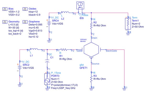
Figure 1.
Schematic for the GFET amplifier large-signal S-parameters (LSSP) analysis.
Simulations are run in the Advanced Design System—ADS (®Keysight, Inc., Santa Rosa, CA, USA) software environment, which performs a DC analysis to choose the bias point and large-signal S-parameters (LSSP) analysis to take into account the device nonlinearity in the computation of the S-parameters. Figure 2 shows the drain current ID computed by varying the drain-source and gate-source bias voltage. As can be observed by viewing the surface curvature, the saturation of the drain current can be obtained in a certain bias region. Since the choice of the bias point is of great importance to achieve optimum performance [], it was carefully chosen to achieve the maximum intrinsic voltage gain AV = gm gds−1. Searching for the optimal bias point, the applied VDS was intentionally limited to prevent the effects of the carrier velocity saturation and the possible self-heating that intervene in high-field conditions, as these phenomena are not addressed by the model. On this basis, the bias point was set to VGS = −0.2 V, VDS = −1.2 V, as found in []. The output conductance gds on top of the drain current ID output characteristic is shown in Figure 3a, and the transconductance gm on top of the ID transfer curve is shown in Figure 3b.
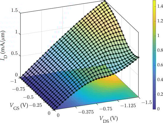
Figure 2.
Surface plot of the drain current ID computed by varying the VGS and VDS.
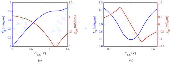
Figure 3.
The DC characteristic of the simulated GFET: (a) the drain current ID (in blue) against the drain-source voltage at VGS = −0.2 V, with superimposed output conductance gds (in red); (b) the drain current ID (in blue) against the gate-source voltage at VDS = −1.2 V, with superimposed transconductance gm (in red).
2.5. Validation of the Simulated GFET Behaviour
In order to validate the simulation results, the fT and fMAX obtained by the circuit simulator for the nominal design of the GFET were compared with the measured values reported in []. For this purpose, the analysis was performed by biasing the transistor at VGS = −0.1 V, VDS = −1.2 V, as reported in the paper. In addition, the values computed by means of the small-signal relations reported in Equations (5) and (6) are also reported. As can be observed, the results obtained by using Equations (5) and (6) agree neither with the experiment nor with the simulation, probably due to the nonlinear behaviour of the device and to the model being based on nonreciprocal capacitances. The simulation results replicate the measurements quite well, especially concerning the fMAX, as can be seen in Table 3. Differences between the simulation and the measurement can be caused by the imperfect value attributed to some of the graphene-related input parameters reported in Table 2, and can be reduced by applying optimization techniques to find the parameters’ values that improve the fitting of the measured current curves.
Table 3.
Simulated and measured fT, fMAX at VGS = −0.1 V, VDS = −1.2 V.
The simulated h21 and MAG at the optimal bias point VGS = −0.2 V, VDS = −1.2 V, instead, return a nominal value for the fT and fMAX of fT,n = 29.40 GHz and fMAX,n = 14.84 GHz and are shown in Figure 4.
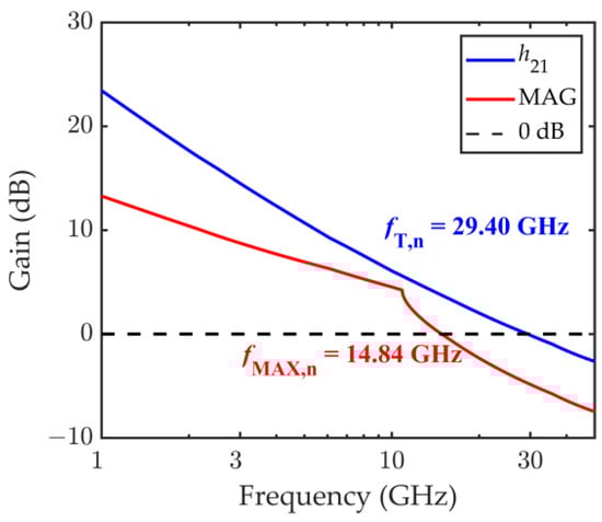
Figure 4.
Short-circuit current gain h21 and maximum available gain MAG computed in correspondence of the nominal set of input parameters, at the bias point VGS = −0.2 V, VDS = −1.2 V. The nominal cut-off frequency is fT,n = 29.40 GHz, and the nominal maximum oscillation frequency is fMAX,n = 14.84 GHz.
3. Tolerance Analysis Results
3.1. fT Sensitivity
To extract the fT from the simulation results, the short-circuit current gain h21 was computed for the 27 combinations of the input factors, and the scattered data is plotted against the factors in Figure 5a, showing the main effects plot, and against the factor-mixed products in Figure 5b, showing the interaction effects plot. By looking at Figure 5 it can be concluded that the transition frequency fT is by far more sensitive to the channel length L rather than to the other parameters, as the L factor variation causes the highest location shift of the mean performance, indicated by the blue dots for each level taken by the input factors. This result confirms expectations, since the peak cut-off frequency is reported to have a 1/L dependence in FETs with short gate lengths, and a 1/L2 dependence in FETs with long gate lengths []. The two other factors have the same influence on the fT, and both are much less effective than L. As can be observed from the fT main effects and interaction effects values reported in Table 4, the main effect of the channel length L, ME3 = −7.11, is by far the highest contribution to the fT variability. The interactions between the channel length L and the other two factors (i.e., IE13 and IE23) are very similar, and comparable to the main effects of tOX and W, ME1, and ME2. They are less than 10% of the main effect of the L, meaning that W and tOX and their interactions with L impact the response variability by less than 10% of the impact of L.
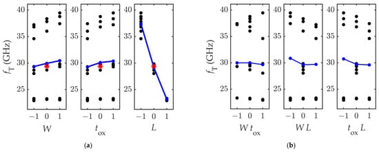
Figure 5.
Computed values of fT against (a) the input factors and (b) the factor-mixed products. The blue lines connect the fT average values, and the red star marks the response computed at the nominal set of the input parameters.
Table 4.
fT main effects and interaction effects.
Concerning the linearity of the response, the fT variation induced by the variation of the factors of 10% is approximately linear; in fact, the blue line connecting the average fT computed at the different levels of the input factors is pretty straight, and closely passes the nominal response fT,n.
To account for the slight nonlinearity of the response variable in the regression model, the interaction effects shown in Figure 5b can be considered. The interaction effects are computed by calculating the slope of the line connecting the average values of fT computed when the product of the coded factors equals −1 and +1. The introduction of such effects can model the small curvatures in the response.
On this basis, the fT variability can be modelled by:
where W, tOX, and L are varying between −1 and +1, following the coding reported in Table 1.
fT = 29.4 + 0.557 W + 0.549 tOX − 7.11 L − 0.166 W tOX − 0.575 W L − 0.57 tOX L
3.2. fMAX Sensitivity
The fMAX variation in response to the variation of the input factors is shown in Figure 6a,b, which report the main effects plot and the interaction effect plot, respectively. As in the previous case, the blue lines connect the fMAX average values computed in correspondence of each level of the factors, and the red star indicates the nominal response fMAX,n.
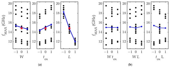
Figure 6.
Computed values of fMAX against (a) the input factors and (b) the factor-mixed products. The blue lines connect the fMAX average values, and the red star marks the response computed at the nominal set of the input parameters.
By looking at Figure 6, it can be observed that the factor most influential on the fMAX is, as for the fT, the channel length L. However, contrarily to what was observed for fT, the increase of the channel width W causes a decrease of the fMAX. Another noticeable result is that, in this case, the response dependence on the three factors is very linear. In fact, the plots in Figure 6b show that there is no interaction between W and tOX, and that the interaction between W and L is one order of magnitude smaller than the lowest main effect. Moreover, while for the fT the factors W and tOX had a similar impact on the response, for the fMAX it is observed that the tOX is the second most influential parameter, as its main effect doubles the main effect of W, and is ≈20% the main effect of L. This is clearer by observing the computed values of the main effects and interaction effects reported in Table 5.
Table 5.
fMAX main effects and interaction effects.
These values allow extracting the linear regression model representing the variability of the PF fMAX, which is:
fMAX = 14.84 – 0.356 W + 0.615 tOX − 3.14 L + 0.042 W L − 0.263 tOX L
4. Conclusions
An analysis of the impact on the fabrication-related tolerances of the GFET geometrical parameters was performed by means of designed circuit simulations.
The factor variation most influential on the transition frequency and the maximum oscillation frequency uniformity for a GFET-based common-source amplifier is the channel length L, coherently with the concept that the transistor high-frequency limit is inversely proportional to the time the carriers need to cross the channel. Reducing the channel length has great benefits on the transition frequency improvement and helps to improve the maximum frequency, too. Hence, being able to control the channel length reliably and applying all the possible measures to limit the occurrence of any uncontrollable phenomenon interfering with the channel length accuracy is the best way to reduce unwanted fluctuations of the fabricated transistors’ cut-off frequency, and therefore improve the intra-wafer and inter-wafer performance uniformity. The improvement provided by increasing the accuracy of the other geometrical parameters, instead, is very limited. In fact, this analysis has shown that the impact of the channel width W and the top oxide thickness tOX on the fT is the same, and it is less than 10% of the impact of the channel length L. The interaction between L and the other two factors has an impact comparable to the W and tOX main effect, and must therefore be included in the regression model for the fT. Concerning the fMAX, the tOX is the second most influential factor, with the main effect that is about 20% of the L main effect. The W impacts on the fMAX by less than 10% the impact of the L. A first-order regression model accounting for interaction between the factors is provided for both the considered performance indicators, allowing both the prediction of the expected variability when the tolerance of process parameters is known, and the definition of a region of acceptability for the factors’ tolerances when the variability of the observed performance is constrained.
In conclusion, the reduction of the variability of W and tOX would improve the uniformity of the fT and fMAX far less than a reduction of the variability of L by an equal percentage amount. The quantitative evaluation of this improvement can be done by using the provided mathematical relations between the quantities of interest. These considerations can support the cost/benefit analysis for the planning of investments to improve the ability of the manufacturing process to control the geometric parameters.
Further work includes the tolerance analysis of different GFET devices found in the literature, in order to compare the robustness of different device layouts and different processes to the fabrication-related tolerances. Moreover, the impact of graphene quality on the RF performance could be assessed quantitatively, providing the model with different inputs depending on the graphene quality indicators.
Author Contributions
Conceptualization, M.L.M.; methodology, M.L.M. and P.L.; software, M.L.M.; investigation, M.L.M. and P.L.; visualization, M.L.M.; writing—original draft preparation, M.L.M.; writing—review and editing, P.L. and V.T.; supervision, P.L. and V.T.; project administration, P.L.; funding acquisition, P.L. All authors have read and agreed to the published version of the manuscript.
Funding
This project has received funding from the European Union’s Horizon 2020 research and innovation programme under the grant agreement GrapheneCore3 881603.
Acknowledgments
The authors acknowledge Francisco Pasadas for providing the GFET compact model used for the circuit simulations.
Conflicts of Interest
The authors declare no conflict of interest.
References
- Passlack, M.; Zurcher, P.; Rajagopalan, K.; Droopad, R.; Abrokwah, J.; Tutt, M.; Park, Y.B.; Johnson, E.; Hartin, O.; Zlotnicka, A.; et al. High mobility III-V MOSFETs for RF and digital applications. In Proceedings of the 2007 IEEE International Electron Devices Meeting, Washington, DC, USA, 10–12 December 2007; pp. 621–624. [Google Scholar]
- Barratt, C.A. III-V Semiconductors, a History in RF Applications. ECS Trans. 2009, 19, 79. [Google Scholar] [CrossRef]
- Saravanan, M.; Parthasarathy, E. A review of III-V Tunnel Field Effect Transistors for future ultra low power digital/analog applications. Microelectron. J. 2021, 114, 105102. [Google Scholar] [CrossRef]
- Ajayan, J.; Nirmal, D. A review of InP/InAlAs/InGaAs based transistors for high frequency applications. Superlattices Microstruct. 2015, 86, 1–19. [Google Scholar] [CrossRef]
- Ferrari, A.C.; Bonaccorso, F.; Fal’ko, V.; Novoselov, K.S.; Roche, S.; Bøggild, P.; Borini, S.; Koppens, F.H.L.; Palermo, V.; Pugno, N.; et al. Science and technology roadmap for graphene, related two-dimensional crystals, and hybrid systems. Nanoscale 2015, 7, 4598–4810. [Google Scholar] [CrossRef] [Green Version]
- Schwierz, F. Graphene transistors. Nat. Nanotechnol. 2010, 5, 487–496. [Google Scholar] [CrossRef]
- Fiori, G.; Bonaccorso, F.; Iannaccone, G.; Palacios, T.; Neumaier, D.; Seabaugh, A.; Banerjee, S.K.; Colombo, L. Electronics based on two-dimensional materials. Nat. Nanotechnol. 2014, 9, 768–779. [Google Scholar] [CrossRef] [PubMed]
- Fiori, G.; Neumaier, D.; Szafranek, B.N.; Iannaccone, G. Bilayer graphene transistors for analog electronics. IEEE Trans. Electron Devices 2014, 61, 729–733. [Google Scholar] [CrossRef]
- Neumaier, D.; Zirath, H. High frequency graphene transistors: Can a beauty become a cash cow? 2D Mater. 2015, 2, 030203. [Google Scholar] [CrossRef]
- Lemme, M.C.; Echtermeyer, T.J.; Baus, M.; Kurz, H. A graphene field-effect device. IEEE Electron Device Lett. 2007, 28, 282–284. [Google Scholar] [CrossRef] [Green Version]
- Meric, I.; Han, M.Y.; Young, A.F.; Ozyilmaz, B.; Kim, P.; Shepard, K.L. Current saturation in zero-bandgap, top-gated graphene field-effect transistors. Nat. Nanotechnol. 2008, 3, 654–659. [Google Scholar] [CrossRef]
- Meric, I.; Dean, C.; Young, A.; Hone, J.; Kim, P.; Shepard, K.L. Graphene field-effect transistors based on boron nitride gate dielectrics. In Proceedings of the Technical Digest-International Electron Devices Meeting, IEDM, San Francisco, CA, USA, 6–8 December 2010. [Google Scholar]
- Peng, S.; Jin, Z.; Ma, P.; Yu, G.; Shi, J.; Zhang, D.; Chen, J.; Liu, X.; Ye, T. Heavily p-type doped chemical vapor deposition graphene field-effect transistor with current saturation. Appl. Phys. Lett. 2013, 103, 223505. [Google Scholar] [CrossRef]
- Szafranek, B.N.; Fiori, G.; Schall, D.; Neumaier, D.; Kurz, H. Current saturation and voltage gain in bilayer graphene field effect transistors. Nano Lett. 2012, 12, 1324–1328. [Google Scholar] [CrossRef] [Green Version]
- Lin, Y.-M.; Jenkins, K.A.; Valdes-Garcia, A.; Small, J.P.; Farmer, D.B.; Avouris, P. Operation of graphene transistors at gigahertz frequencies. Nano Lett. 2008, 9, 422–426. [Google Scholar] [CrossRef] [PubMed] [Green Version]
- Wu, Y.; Lin, Y.M.; Bol, A.A.; Jenkins, K.A.; Xia, F.; Farmer, D.B.; Zhu, Y.; Avouris, P. High-frequency, scaled graphene transistors on diamond-like carbon. Nature 2011, 472, 74–78. [Google Scholar] [CrossRef] [PubMed]
- Meric, I.; Dean, C.R.; Han, S.J.; Wang, L.; Jenkins, K.A.; Hone, J.; Shepard, K.L. High-frequency performance of graphene field effect transistors with saturating IV-characteristics. In Proceedings of the Technical Digest-International Electron Devices Meeting, IEDM, Washington, DC, USA, 5–7 December 2011. [Google Scholar]
- Rawat, B.; Paily, R. Analysis of graphene tunnel field-effect transistors for analog/RF applications. IEEE Trans. Electron Devices 2015, 62, 2663–2669. [Google Scholar] [CrossRef]
- Lyu, H.; Lu, Q.; Liu, J.; Wu, X.; Zhang, J.; Li, J.; Niu, J.; Yu, Z.; Wu, H.; Qian, H. Deep-submicron graphene field-effect transistors with state-of-art fmax. Sci. Rep. 2016, 6, 35717. [Google Scholar] [CrossRef] [Green Version]
- Bonmann, M.; Asad, M.; Yang, X.; Generalov, A.; Vorobiev, A.; Banszerus, L.; Stampfer, C.; Otto, M.; Neumaier, D.; Stake, J. Graphene field-effect transistors with high extrinsic fT and fmax. IEEE Electron Device Lett. 2019, 40, 131–134. [Google Scholar] [CrossRef] [Green Version]
- Vorobiev, A.; Bonmann, M.; Asad, M.; Yang, X.; Stake, J.; Banszerus, L.; Stampfer, C.; Otto, M.; Neumaier, D. Graphene field-effect transistors for millimeter wave amplifiers. In Proceedings of the 2019 44th International Conference on Infrared, Millimeter, and Terahertz Waves (IRMMW-THz), Paris, France, 1–6 September 2019. [Google Scholar] [CrossRef] [Green Version]
- Liao, L.; Lin, Y.-C.; Bao, M.; Cheng, R.; Bai, J.; Liu, Y.; Qu, Y.; Wang, K.L.; Huang, Y.; Duan, X. High-speed graphene transistors with a self-aligned nanowire gate. Nature 2010, 467, 305–308. [Google Scholar] [CrossRef] [PubMed]
- Wu, Y.; Jenkins, K.A.; Valdes-Garcia, A.; Farmer, D.B.; Zhu, Y.; Bol, A.A.; Dimitrakopoulos, C.; Zhu, W.; Xia, F.; Avouris, P.; et al. State-of-the-art graphene high-frequency electronics. Nano Lett. 2012, 12, 3062–3067. [Google Scholar] [CrossRef]
- Guo, Z.; Dong, R.; Chakraborty, P.S.; Lourenco, N.; Palmer, J.; Hu, Y.; Ruan, M.; Hankinson, J.; Kunc, J.; Cressler, J.D.; et al. Record maximum oscillation frequency in C-face epitaxial graphene transistors. Nano Lett. 2013, 13, 942–947. [Google Scholar] [CrossRef] [Green Version]
- Giubileo, F.; Di Bartolomeo, A. The role of contact resistance in graphene field-effect devices. Prog. Surf. Sci. 2017, 92, 143–175. [Google Scholar] [CrossRef] [Green Version]
- Giubileo, F.; Di Bartolomeo, A.; Martucciello, N.; Romeo, F.; Iemmo, L.; Romano, P.; Passacantando, M. Contact resistance and channel conductance of graphene field-effect transistors under low-energy electron irradiation. Nanomaterials 2016, 6, 206. [Google Scholar] [CrossRef] [PubMed] [Green Version]
- Farmer, D.B.; Valdes-Garcia, A.; Dimitrakopoulos, C.; Avouris, P. Impact of gate resistance in graphene radio frequency transistors. Appl. Phys. Lett. 2012, 101, 143503. [Google Scholar] [CrossRef]
- Wu, Y.; Zou, X.; Sun, M.; Cao, Z.; Wang, X.; Huo, S.; Zhou, J.; Yang, Y.; Yu, X.; Kong, Y.; et al. 200 GHz maximum oscillation frequency in CVD graphene radio frequency transistors. ACS Appl. Mater. Interfaces 2016, 8, 25645–25649. [Google Scholar] [CrossRef]
- Wang, H.; Hsu, A.L.; Palacios, T. Graphene electronics for RF applications. IEEE Microw. Mag. 2012, 13, 114–125. [Google Scholar] [CrossRef]
- Zhang, C.X.; Wang, B.; Duan, G.X.; Zhang, E.X.; Fleetwood, D.M.; Alles, M.L.; Schrimpf, R.D.; Rooney, A.P.; Khestanova, E.; Auton, G.; et al. Total ionizing dose effects on hBN encapsulated graphene devices. IEEE Trans. Nucl. Sci. 2014, 61, 2868–2873. [Google Scholar] [CrossRef]
- Paddubskaya, A.; Batrakov, K.; Khrushchinsky, A.; Kuten, S.; Plyushch, A.; Stepanov, A.; Remnev, G.; Shvetsov, V.; Baah, M.; Svirko, Y.; et al. Outstanding radiation tolerance of supported graphene: Towards 2D Sensors for the space millimeter radioastronomy. Nanomaterials 2021, 11, 170. [Google Scholar] [CrossRef]
- Childres, I.; Jauregui, L.A.; Foxe, M.; Tian, J.; Jalilian, R.; Jovanovic, I.; Chen, Y.P. Effect of electron-beam irradiation on graphene field effect devices. Appl. Phys. Lett. 2010, 97, 173109. [Google Scholar] [CrossRef] [Green Version]
- Perruisseau-Carrier, J. Graphene for antenna applications: Opportunities and challenges from microwaves to THz. In Proceedings of the 2012 Loughborough Antennas & Propagation Conference (LAPC), Loughborough, UK, 12–13 November 2012. [Google Scholar] [CrossRef] [Green Version]
- Yang, X.; Vorobiev, A.; Yang, J.; Jeppson, K.; Stake, J. A Linear-Array of 300-GHz Antenna Integrated GFET Detectors on a Flexible Substrate. IEEE Trans. Terahertz Sci. Technol. 2020, 10, 554–557. [Google Scholar] [CrossRef]
- Han, S.-J.J.; Garcia, A.V.; Oida, S.; Jenkins, K.A.; Haensch, W. Graphene radio frequency receiver integrated circuit. Nat. Commun. 2014, 5, 1–6. [Google Scholar] [CrossRef]
- Bonmann, M.; Andersson, M.A.; Zhang, Y.; Yang, X.; Vorobiev, A.; Stake, J. An Integrated 200-GHz Graphene FET Based Receiver. In Proceedings of the International Conference on Infrared, Millimeter, and Terahertz Waves, IRMMW-THz, Nagoya, Japan, 9–14 September 2018; Volume 2018. [Google Scholar]
- Saeed, M.; Hamed, A.; Wang, Z.; Shaygan, M.; Neumaier, D.; Negra, R. Graphene integrated circuits: New prospects towards receiver realisation. Nanoscale 2018, 10, 93–99. [Google Scholar] [CrossRef]
- Sensale-Rodriguez, B.; Fang, T.; Yan, R.; Kelly, M.M.; Jena, D.; Liu, L.; Xing, H. Unique prospects for graphene-based terahertz modulators. Appl. Phys. Lett. 2011, 99, 113104. [Google Scholar] [CrossRef] [Green Version]
- Sensale-Rodriguez, B.; Yan, R.; Kelly, M.M.; Fang, T.; Tahy, K.; Hwang, W.S.; Jena, D.; Liu, L.; Xing, H.G. Broadband graphene terahertz modulators enabled by intraband transitions. Nat. Commun. 2012, 3, 1–7. [Google Scholar] [CrossRef] [PubMed]
- Phare, C.T.; Daniel Lee, Y.-H.; Cardenas, J.; Lipson, M. Graphene electro-optic modulator with 30 GHz bandwidth. Nat. Photonics 2015, 9, 511–514. [Google Scholar] [CrossRef]
- Habibpour, O.; He, Z.S.; Strupinski, W.; Rorsman, N.; Ciuk, T.; Ciepielewski, P.; Zirath, H. Graphene FET gigabit ON-OFF keying demodulator at 96 GHz. IEEE Electron Device Lett. 2016, 37, 333–336. [Google Scholar] [CrossRef]
- Dalir, H.; Xia, Y.; Wang, Y.; Zhang, X. Athermal broadband graphene optical modulator with 35 GHz Speed. ACS Photonics 2016, 3, 1564–1568. [Google Scholar] [CrossRef]
- Ahmadivand, A.; Gerislioglu, B.; Ramezani, Z. Gated graphene island-enabled tunable charge transfer plasmon terahertz metamodulator. Nanoscale 2019, 11, 8091–8095. [Google Scholar] [CrossRef]
- Hong, S.K.; Kim, K.Y.; Kim, T.Y.; Kim, J.H.; Park, S.W.; Kim, J.H.; Cho, B.J. Electromagnetic interference shielding effectiveness of monolayer graphene. Nanotechnology 2012, 23, 455704. [Google Scholar] [CrossRef]
- Han, S.J.; Jenkins, K.A.; Valdes Garcia, A.; Franklin, A.D.; Bol, A.A.; Haensch, W. High-frequency graphene voltage amplifier. Nano Lett. 2011, 11, 3690–3693. [Google Scholar] [CrossRef]
- Hanna, T.; Deltimple, N.; Khenissa, M.S.; Pallecchi, E.; Happy, H.; Frégonèse, S. 2.5 GHz integrated graphene RF power amplifier on SiC substrate. Solid. State. Electron. 2017, 127, 26–31. [Google Scholar] [CrossRef]
- Hamed, A.; Asad, M.; Wei, M.-D.; Vorobiev, A.; Stake, J.; Negra, R. Integrated 10-GHz Graphene FET Amplifier. IEEE J. Microw. 2021, 1, 821–826. [Google Scholar] [CrossRef]
- Yu, C.; He, Z.; Song, X.; Gao, X.; Liu, Q.; Zhang, Y.; Yu, G.; Han, T.; Liu, C.; Feng, Z.; et al. Field effect transistors and low noise amplifier MMICs of monolayer graphene. IEEE Electron Device Lett. 2021, 42, 268–271. [Google Scholar] [CrossRef]
- Wang, H.; Hsu, A.; Wu, J.; Kong, J.; Palacios, T. Graphene-based ambipolar RF mixers. IEEE Electron Device Lett. 2010, 31, 906–908. [Google Scholar] [CrossRef]
- Habibpour, O.; Cherednichenko, S.; Vukusic, J.; Yhland, K.; Stake, J. A subharmonic graphene FET mixer. IEEE Electron Device Lett. 2012, 33, 71–73. [Google Scholar] [CrossRef] [Green Version]
- Andersson, M.A.; Zhang, Y.; Stake, J. A 185-215-GHz subharmonic resistive graphene FET integrated mixer on silicon. IEEE Trans. Microw. Theory Tech. 2017, 65, 165–172. [Google Scholar] [CrossRef] [Green Version]
- Schall, D.; Otto, M.; Neumaier, D.; Kurz, H. Integrated ring oscillators based on high-performance graphene inverters. Sci. Rep. 2013, 3, 1–5. [Google Scholar] [CrossRef]
- Guerriero, E.; Polloni, L.; Bianchi, M.; Behnam, A.; Carrion, E.; Rizzi, L.G.; Pop, E.; Sordan, R. Gigahertz integrated graphene ring oscillators. ACS Nano 2013, 7, 5588–5594. [Google Scholar] [CrossRef]
- Safari, A.; Dousti, M. Ring oscillators based on monolayer graphene FET. Analog Integr. Circuits Signal Process. 2020, 102, 637–644. [Google Scholar] [CrossRef]
- Coletti, C.; Romagnoli, M.; Giambra, M.A.; Mišeikis, V.; Pezzini, S.; Marconi, S.; Montanaro, A.; Fabbri, F.; Sorianello, V.; Ferrari, A.C. Wafer-scale integration of graphene-based photonic devices. ACS Nano 2021, 15, 3171–3187. [Google Scholar] [CrossRef]
- Neumaier, D.; Pindl, S.; Lemme, M.C. Integrating graphene into semiconductor fabrication lines. Nat. Mater. 2019, 18, 525–529. [Google Scholar] [CrossRef] [Green Version]
- Paul, B.C.; Fujita, S.; Okajima, M.; Lee, T.H.; Wong, H.S.P.; Nishi, Y. Impact of a process variation on nanowire and nanotube device performance. IEEE Trans. Electron Devices 2007, 54, 2369–2376. [Google Scholar] [CrossRef]
- Taguchi, G. System of Experimental Design: Engineering Methods to Optimize Quality and Minimize Costs; UNIPUB/Kraus International Publications: New York, NY, USA, 1987; ISBN 978-0527916213. [Google Scholar]
- Hinkelmann, K. Design and Analysis of Experiments; American Psychological Association: Washington, DC, USA, 2012; Volume 3. [Google Scholar]
- Montgomery, D.C. Design and Analysis of Experiments, 9th ed.; John Wiley & Sons: Hoboken, NJ, USA, 2017; ISBN 9781119113478. [Google Scholar]
- Pasadas, F.; Jiménez, D. Large-signal model of graphene field-effect transistors-part I: Compact modeling of GFET intrinsic capacitances. IEEE Trans. Electron Devices 2016, 63, 2936–2941. [Google Scholar] [CrossRef] [Green Version]
- Lamberti, P.; La Mura, M.; Pasadas, F.; Jiménez, D.; Tucci, V. Tolerance analysis of a GFET transistor for aerospace and aeronautical application. In Proceedings of the IOP Conference Series: Materials Science and Engineering, Salerno, Italy, 2–4 September 2020; Volume 1024. [Google Scholar]
- Spinelli, G.; Lamberti, P.; Tucci, V.; Pasadas, F.; Jiménez, D. Sensitivity analysis of a graphene field-effect transistors by means of design of experiments. Math. Comput. Simul. 2020, 183, 187–197. [Google Scholar] [CrossRef]
- Jmai, B.; Silva, V.; Mendes, P.M. 2D electronics based on graphene field effect transistors: Tutorial for modelling and simulation. Micromachines 2021, 12, 979. [Google Scholar] [CrossRef] [PubMed]
- Cabral, P.D.; Domingues, T.; Machado, G.; Chicharo, A.; Cerqueira, F.; Fernandes, E.; Athayde, E.; Alpuim, P.; Borme, J. Clean-room lithographical processes for the fabrication of graphene biosensors. Materials 2020, 13, 5728. [Google Scholar] [CrossRef]
- Gupta, A.; Fang, P.; Song, M.; Lin, M.R.; Wollesen, D.; Chen, K.; Hu, C. Accurate determination of ultrathin gate oxide thickness and effective polysilicon doping of CMOS devices. IEEE Electron Device Lett. 1997, 18, 580–582. [Google Scholar] [CrossRef]
- La Mura, M.; Bagolini, A.; Lamberti, P.; Savoia, A.S. Impact of the variability of microfabrication process parameters on CMUTs performance. In Proceedings of the IEEE International Ultrasonics Symposium, IUS, Las Vegas, NV, USA, 7–11 September 2020. [Google Scholar]
- Lamberti, P.; Sarto, M.S.; Tucci, V.; Tamburrano, A. Robust design of high-speed interconnects based on an MWCNT. IEEE Trans. Nanotechnol. 2012, 11, 799–807. [Google Scholar] [CrossRef]
- Lamberti, P.; Tucci, V. Impact of the variability of the process parameters on CNT-based nanointerconnects performances: A comparison between SWCNTs bundles and MWCNT. IEEE Trans. Nanotechnol. 2012, 11, 924–933. [Google Scholar] [CrossRef]
- Pasadas, F.; Jiménez, D. Large-signal model of graphene field-effect transistors-part II: Circuit performance benchmarking. IEEE Trans. Electron Devices 2016, 63, 2942–2947. [Google Scholar] [CrossRef] [Green Version]
- Pozar, D.M. Microwave Engineering, 4th ed.; John Wiley & Sons Inc.: Hoboken, NJ, USA, 2012; pp. 1–756. [Google Scholar]
- Fiori, G.; Iannaccone, G. Multiscale modeling for graphene-based nanoscale transistors. Proc. IEEE 2013, 101, 1653–1669. [Google Scholar] [CrossRef]
- Thiele, S.A.; Schaefer, J.A.; Schwierz, F. Modeling of graphene metal-oxide-semiconductor field-effect transistors with gapless large-area graphene channels. J. Appl. Phys. 2010, 107. [Google Scholar] [CrossRef]
- Rodriguez, S.; Vaziri, S.; Smith, A.; Fregonese, S.; Ostling, M.; Lemme, M.C.; Rusu, A. A comprehensive graphene FET model for circuit design. IEEE Trans. Electron Devices 2014, 61, 1199–1206. [Google Scholar] [CrossRef]
- Asad, M.; Bonmann, M.; Yang, X.; Vorobiev, A.; Jeppson, K.; Banszerus, L.; Otto, M.; Stampfer, C.; Neumaier, D.; Stake, J. The dependence of the high-frequency performance of graphene field-effect transistors on channel transport properties. IEEE J. Electron Devices Soc. 2020, 8, 457–464. [Google Scholar] [CrossRef]
- Fregonese, S.; Magallo, M.; Maneux, C.; Happy, H.; Zimmer, T. Scalable electrical compact modeling for graphene FET transistors. IEEE Trans. Nanotechnol. 2013, 12, 539–546. [Google Scholar] [CrossRef]
- Landauer, G.M.; Jimenez, D.; Gonzalez, J.L. An accurate and verilog-a compatible compact model for graphene field-effect transistors. IEEE Trans. Nanotechnol. 2014, 13, 895–904. [Google Scholar] [CrossRef]
- Aguirre-Morales, J.D.; Fregonese, S.; Mukherjee, C.; Wei, W.; Happy, H.; Maneux, C.; Zimmer, T. A Large-signal monolayer graphene field-effect transistor compact model for RF-circuit applications. IEEE Trans. Electron Devices 2017, 64, 4302–4309. [Google Scholar] [CrossRef]
- Han, S.J.; Reddy, D.; Carpenter, G.D.; Franklin, A.D.; Jenkins, K.A. Current saturation in submicrometer graphene transistors with thin gate dielectric: Experiment, simulation, and theory. ACS Nano 2012, 6, 5220–5226. [Google Scholar] [CrossRef]
- Parrish, K.N.; Akinwande, D. Impact of contact resistance on the transconductance and linearity of graphene transistors. Appl. Phys. Lett. 2011, 98, 183505. [Google Scholar] [CrossRef]
- Chauhan, J.; Liu, L.; Lu, Y.; Guo, J. A computational study of high-frequency behavior of graphene field-effect transistors. J. Appl. Phys. 2012, 111. [Google Scholar] [CrossRef]
Publisher’s Note: MDPI stays neutral with regard to jurisdictional claims in published maps and institutional affiliations. |
© 2021 by the authors. Licensee MDPI, Basel, Switzerland. This article is an open access article distributed under the terms and conditions of the Creative Commons Attribution (CC BY) license (https://creativecommons.org/licenses/by/4.0/).