Article

Tailoring the Structural and Optical Properties of Germanium Telluride Phase-Change Materials by Indium Incorporation

1
Center for Alloy Innovation and Design (CAID), State Key Laboratory for Mechanical Behavior of Materials, Xi’an Jiaotong University, Xi’an 710049, China
2
Pazhou Lab, Pengcheng National Laboratory in Guangzhou, Guangzhou 510320, China
*
Author to whom correspondence should be addressed.
Nanomaterials 2021, 11(11), 3029; https://doi.org/10.3390/nano11113029
Submission received: 10 October 2021 / Revised: 5 November 2021 / Accepted: 10 November 2021 / Published: 12 November 2021
(This article belongs to the Special Issue Synthesis, Properties and Applications of Germanium Chalcogenides)

Abstract

:
Chalcogenide phase-change materials (PCMs) based random access memory (PCRAM) enter the global memory market as storage-class memory (SCM), holding great promise for future neuro-inspired computing and non-volatile photonic applications. The thermal stability of the amorphous phase of PCMs is a demanding property requiring further improvement. In this work, we focus on indium, an alloying ingredient extensively exploited in PCMs. Starting from the prototype GeTe alloy, we incorporated indium to form three typical compositions along the InTe-GeTe tie line: InGe3Te4, InGeTe2 and In3GeTe4. The evolution of structural details, and the optical properties of the three In-Ge-Te alloys in amorphous and crystalline form, was thoroughly analyzed via ab initio calculations. This study proposes a chemical composition possessing both improved thermal stability and sizable optical contrast for PCM-based non-volatile photonic applications.

1. Introduction

Non-volatile memory (NVM) is a rising technology that allows for high-density data storage and fast data processing [1,2,3,4,5,6]. Phase-change materials (PCMs)-based random access memory (PCRAM) is a leading NVM candidate with successful stand-alone memory products such as Intel Optane. By improving its thermal stability, PCRAM is also a promising candidate for embedded memory [7,8]. As announced by STMicroelectronics, PCRAM will be used as embedded memory, replacing Flash memory, for their future microcontroller units (MCU) for the automotive industry [7]. Moreover, PCRAM is also being exploited for more advanced applications, including neuro-inspired computing [9,10,11,12,13,14,15], stochasticity-based computing [16,17], flexible electronics [18], optical displays [19,20,21], all-optical computers [22,23,24,25,26], low-loss optical modulators [27], metasurfaces [28,29,30,31,32] and others [33,34].
PCMs can be switched rapidly and reversibly between their amorphous and crystalline phases via Joule heating induced by electrical or optical pulses [1,35]. The notable contrast in either electrical resistivity or optical reflectivity between each phase is utilized to encode digital information [1]. Several demanding requirements, such as high programming speed, good thermal stability, low power consumption, stable property contrast window and long cycling endurance, have to be well satisfied for high-performance PCRAM. Germanium chalcogenides, in particular, GeTe and GeTe-Sb2Te3 pseudo-binary compounds (GST), especially Ge2Sb2Te5 [36], are one of the most successful material families that could meet these challenging requirements simultaneously. Doping and alloying are frequently used to tailor the material properties for faster speed and/or better retention temperature, targeting different application scenarios [37,38,39,40,41,42,43,44].
For decades, indium has been an important alloying element used in rewritable optical data storage products [45]. The flagship PCM is AgInSbTe [45,46,47,48]. Recently, indium-alloyed GeTe [49,50,51,52] and GST [53,54] were reported, and their enhanced amorphous stability makes them suitable candidates for high-temperature PCRAM applications. In addition, indium forms a unique PCM In3SbTe2 [55,56,57,58,59] that exhibits metallic behavior in its crystalline phase, but semiconducting behaviors in its amorphous phase, in contrast to conventional PCMs, which remain semiconducting during memory programming. It has been suggested that even InTe could also be a potential PCM for non-volatile electronics [53,60]. In this work, we focus on the InTe-GeTe (IGT) tie line, in particular, the three stoichiometric compositions, namely InGe3Te4, InGeTe2 and In3GeTe4. By performing thorough ab initio calculations and chemical bonding analyses, we elucidate the role of indium in altering the structural and optical properties of GeTe.

2. Computational Details

We performed ab initio molecular dynamics (AIMD) simulations based on density functional theory (DFT) to generate melt-quenched amorphous structures [61]. The second-generation Car-Parrinello method [62] as implemented in CP2K package [63] was employed along with Perdew–Burke–Ernzerhof (PBE) functional [64] and the Goedecker pseudopotentials [65]. The canonical NVT ensemble was used and the time step was set at 2 fs. Vienna Ab-initio Simulation Package (VASP) [66] was employed to relax the amorphous structures and crystalline counterparts, prior to the calculations of electronic structure and optical response. For VASP calculations, we applied the PBE functional and projector augmented-wave (PAW) pseudopotentials [67]. The energy cutoff for plane waves was set at 500 eV. Chemical bonding analyses were conducted with the LOBSTER code [68,69,70]. Crystal orbital Hamilton populations (COHP) were applied to separate the covalent interactions into bonding (positive −COHP) and antibonding (negative −COHP) contributions. Bader charges were calculated to evaluate the atomic charge transfer in the structures [71]. Frequency-dependent dielectric matrix was calculated within the independent-particle approximation without considering local field effects and many body effects, which proved to be adequate to account for the optical contrast between crystalline and amorphous PCMs [72,73,74]. The absorption α ( ω ) and reflectivity R ( ω ) can be calculated from the dielectric functions [75]:
α ( ω ) = 2 ω c   ( ε 1 2 + ε 2 2 ε 1 ) 1 2
R ( ω ) = ( n 1 ) 2 + k 2 ( n + 1 ) 2 + k 2
where ε 1 and ε 2 are the real and imaginary parts of the dielectric function. n and k are the refractive index and extinction coefficient, which can be calculated from the dielectric functions:
n ( ω ) = ( ε 1 2 + ε 2 2 + ε 1 2 ) 1 2  
k ( ω ) = ( ε 1 2 + ε 2 2 ε 1 2 ) 1 2
Van der Waals correction based on the Grimme’s D3 method was considered in all AIMD and DFT calculations [76,77]. All the electronic structures, chemical bonding and optical properties were calculated using relaxed structures at zero K with VASP. For standard calculations, only gamma point was used to sample the Brillouin zone of the supercell models, while a 3 × 3 × 3 k-point mesh was used to converge the optical response calculations. For statistics, we built three crystalline and three amorphous models for each composition.

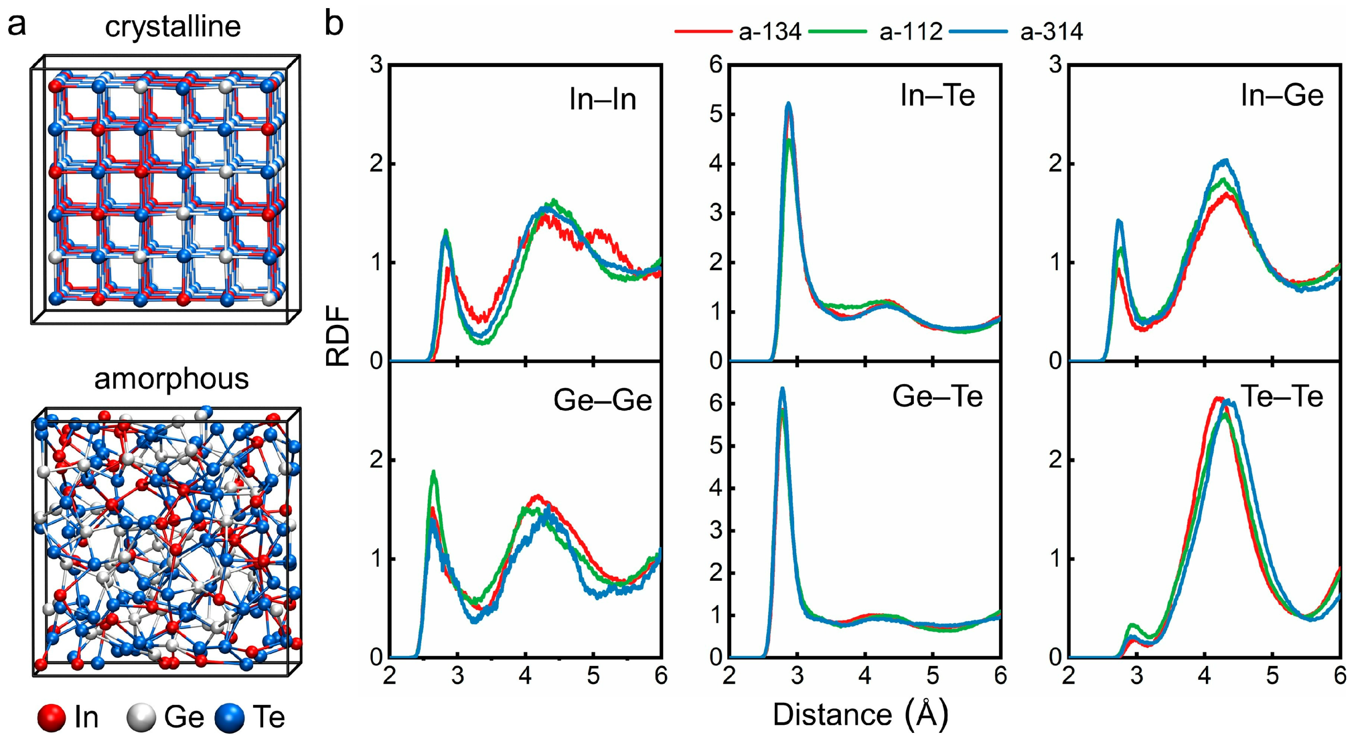
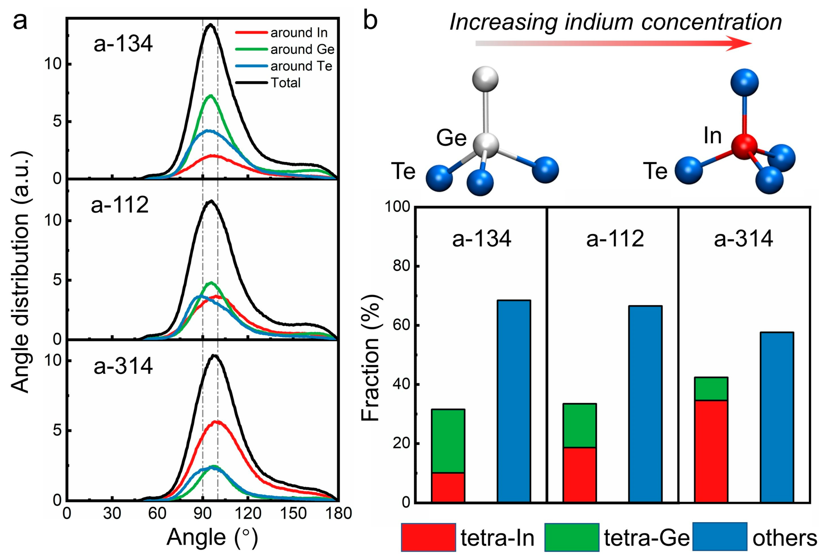
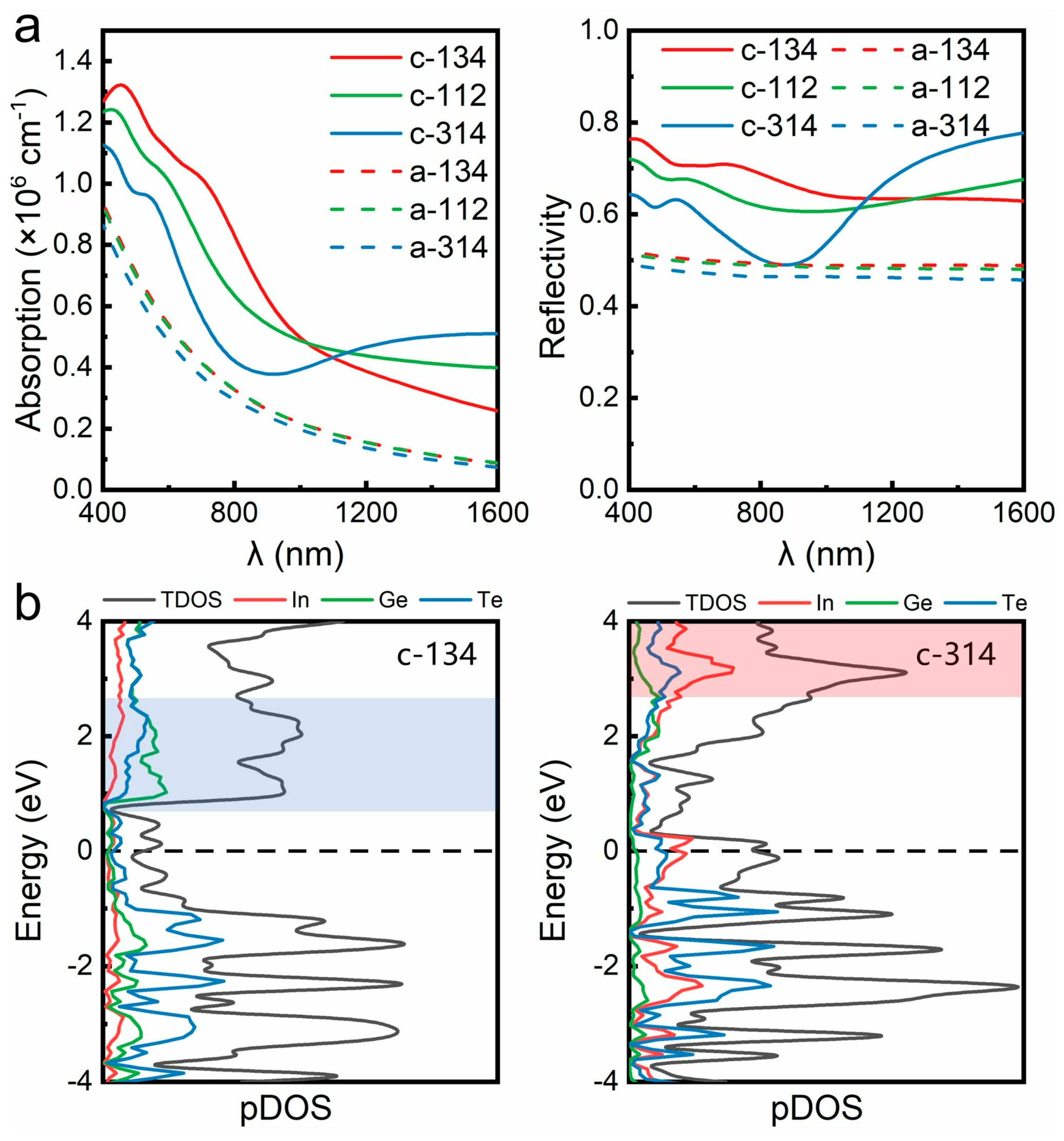
3. Results and Discussion

As reported in Ref. [78], a single-phase rock-salt structure was obtained over a wide compositional range of 8–75 mole% InTe in IGT at ambient conditions, in which Te atoms occupied one sublattice, while Ge and In atoms shared the other one. The three IGT compositions considered in this work, namely InGe3Te4, InGeTe2 and In3GeTe4, fall in this compositional range, and were expected to take the rock-salt structure. To account for the compositional disorder of Ge and In atoms on the cation-like sublattice, we built 3 × 3 × 3 supercells (216 atoms in total) and distributed Ge and In atoms using a quasi-random number generator. Three independent models were considered for each composition. Each supercell model was fully relaxed with respect to both atomic coordinates and cell volume by DFT calculations. The relaxed cell-edge of crystalline (c-) InGe3Te4, InGeTe2 and In3GeTe4 is 18.21, 18.28 and 18.55 Å, respectively. The corresponding unit cell lattice parameters, 6.07, 6.09 and 6.18 Å, are in good agreement with experimental values (5.97, 6.00 and 6.06 Å) [78]. The relaxed structure of c-InGeTe2 is shown in Figure 1a and the structures of the other two compositions are shown in Figure S1.
The relaxed crystalline supercells were then used to generate amorphous (a-) models following a melt–quench protocol [61]. The supercell models were quickly heated to a very high temperature to remove the crystalline order. After randomization at 3000 K for 15 ps, the models were quenched down to and equilibrated at 1200 K, above the melting point of IGT alloys (∼550–750 °C) [49] for 30 ps. Amorphous models were then generated by quenching the liquids down to 300 K with a cooling rate of 12.5 K/ps. During this quenching process, we stopped the simulation after every 100 K, and the simulation box size was increased to reduce the internal stress. Within each temperature window, one NVT calculation was performed using a fixed box size. The model was equilibrated at 300 K for 30 ps. This density value was then used to generate two additional melt-quenched amorphous models for each composition. All three amorphous models showed consistently low pressure values below 3 kbar. The obtained cell edges of amorphous InGe3Te4, InGeTe2 and In3GeTe4 are 18.90, 19.08 and 19.32 Å, respectively. This increase in the cell edge of the amorphous phase is consistent with the trend observed in their crystalline counterparts. Further optimization of the internal stress or the use of the NPT ensemble for melt-quench simulations could potentially lead to some numerical differences in the mass density, but is not expected to alter the amorphous structures much.
The amorphous structure of InGeTe2 is shown in Figure 1a and the snapshots of the other two compositions are in Figure S1. The partial radial distribution functions (RDFs) of each atomic pair in the three amorphous compounds are shown in Figure 1b. The peak positions of the heteropolar bonds In–Te (2.87 Å) and Ge–Te (2.78 Å) are not varied with composition, whereas the homopolar or “wrong” bonds show small shifts. As developed in our previous work [79], the “bond-weighted distribution function (BWDF)” provides direct information on the length of chemical bonds in amorphous IGT alloys (Figure S2). Despite the change in chemical composition, the bond length shows very similar values in amorphous IGT alloys, i.e., Ge–Te 3.20 Å, In–Te 3.40 Å, Ge–Ge 3.20 Å, In–In 3.25 Å and Ge–In 3.40 Å. In all three amorphous IGT alloys, Te–Te shows mostly antibonding interactions. These bond length values are used as cutoffs for the interatomic distance for the following structural analysis.
The angle distribution function (ADF) of the three amorphous structures (Figure 2a) shows that In and Ge atoms mainly form local motifs with the central bond angles ranging from 90° to 109.5°, which corresponds to the bond angles in octahedral and tetrahedral motifs, respectively. As the concentration of indium increases, the ADF peak for indium atoms clearly shifts toward 109.5°, implying an increase in indium-centered tetrahedral motifs. We used bond order parameter q [80] to quantify the fraction of tetrahedral motifs in amorphous IGT alloys. Such parameters are frequently used for the structural analysis of amorphous PCMs [81,82,83]. As shown in Figure 2b, as indium concentration increases, the total fraction of In- and Ge-centered tetrahedral motifs (short as tetra-In and tetra-Ge) increases from 31.6% (a-InGe3Te4), 33.5% (a-InGeTe2) to 42.4% (a-In3GeTe4) in relation to the total number of In and Ge atoms. Specifically, the fraction of tetra-In increases from 10.1%, 18.6% to 34.6%, while the fraction of tetra-Ge decreases from 21.5%, 14.9% to 7.8%. The fraction of tetrahedrons for a-InGeTe2 is smaller than that reported in previous work (38 % in total, with 31.5% for tetra-In and 6.5% for tetra-Ge) [50], due to the different choice of cutoff values for the interatomic distance and the deviation in calculated density values (vdW interactions were included in the current work). The ratios of tetrahedral motifs in amorphous IGT alloys are all higher than that of their parent phase—GeTe, where 25–30% tetrahedral atoms are typically found in the rapidly quenched amorphous phase [84,85,86].
In addition to the increase in the total number of tetrahedral motifs from a-InGe3Te4 to a-In3GeTe4, the local bonding configuration also shows a major difference. Despite the change in chemical compositions, nearly all the tetra-Ge atoms are bonded with at least one Ge or In atom, while the majority of tetra-In atoms are heteropolar-bonded in the three amorphous IGT alloys. To quantify the role of “wrong” bonds, we carried out a projected COHP (pCOHP) analysis. As shown in Figure 3 and Figure S3, the pCOHP of heteropolar-bonded tetra-Ge atoms demonstrates sizable antibonding interactions right below Fermi energy (EF), and the presence of wrong bonds (including Ge–Ge and Ge–In) largely reduces such antibonding contributions, stabilizing the tetrahedral motifs locally. In contrast, the pCOHP of tetra-In atoms with and without wrong bonds mostly shows bonding interactions below EF. These results are consistent with the bonding configuration in the two parent phases, a-GeTe [79] and a-InTe [83], though In–Ge bonds are present in all three amorphous IGT alloys. Since indium atoms do not require homopolar bonds to stabilize tetrahedral motifs, the ratio of tetrahedral units is increased with the indium concentration. As compared to their crystalline counterparts, where all In and Ge atoms are octahedrally bonded, the enlarged structural deviation will enhance the thermal stability of amorphous IGT alloys. This observation is consistent with experimental findings, as the crystallization temperature Tx of doped InGeTe2 [49] and undoped InTe thin films [60] is increased to ∼276 and ∼300 °C, respectively, as compared to that of GeTe Tx ∼190 °C [87].
The calculated density of states (DOS) of the three IGT alloys in both crystalline and amorphous forms are shown in Figure 4a,b. Regarding the crystalline models, the overall DOS profiles are quite similar, and all three alloys exhibit metallic features. By contrast, all three amorphous models are narrow-gap semiconductors. Statistical sampling yields consistent results (Figure S4). The large difference in DOS between the crystalline and amorphous IGT results in a wide resistance contrast window for PCRAM applications [49]. The Bader charge analysis (Figure 4c) details larger net charges for In atoms than for Ge atoms due to the difference in electronegativity. The bimodal feature of the charges of indium atoms is consistent with previous work [50], stemming from different local environments of indium atoms. The enlarged charge transfer in amorphous structures increases the probability of long-distance electromigration under the transient electrical field induced by programming pulses [88], which is detrimental to the cycling endurance of devices [89,90]. For RESET operations, the higher the melting temperature Tm, the greater the power consumption. The melting temperature for IGT alloys has a “W” shape profile, according to the InTe-GeTe phase diagram, which shows that InGeTe2 has a higher melting temperature Tm (740 °C) than GeTe and InTe whose Tm are 715 and 688 °C, respectively [49]. Interestingly, the two other compositions, InGe3Te4 and In3GeTe4, demonstrated reduced Tm (645 and 565 °C). Taking into account all these factors for practical applications, we would suggest keeping the IGT composition within the range of InGeTe2 to In3GeTe4 for balanced device performance.
The enhanced amorphous stability is also useful for non-volatile photonic applications [91], yet the incorporation of indium makes IGT alloys metallic, which could affect the optical contrast between the amorphous and crystalline phase. The significant contrast of ∼30% in the optical reflectivity of PCMs stems from a fundamental change in bonding nature from covalent to metavalent bonding (MVB) upon crystallization [92,93,94,95,96,97,98,99]. However, in comparison with GeTe and GST, which have three p electrons per site (a key feature of MVB), InTe has a deficient number of p electrons, turning the rock-salt phase from semiconducting to metallic. As a result, MVB in IGT alloys is expected to be weakened.
For verification, we carried out optical response calculations using the relaxed crystalline and amorphous IGT structures. We focused on the spectrum range from 400 to 1600 nm, covering both the visible light region (∼400 nm to 800 nm) for optical displays [19,20,21] and the telecom wavelength bands (∼1500 to 1600 nm) for silicon-waveguide-integrated photonic applications [23,24,25,26]. As shown in Figure 5a, the optical absorption and reflectivity profiles vary slightly with the chemical compositions in the amorphous phase, while strong changes are found in the crystalline phase. For InGe3Te4 and InGeTe2, sizable contrast in reflectivity between the crystalline and amorphous phases is observed over the whole spectrum, with an average value ∼20%. However, for In3GeTe4, the contrast in reflectivity nearly vanishes at around ∼900 nm, and it becomes greater below 700 nm, or above 1000 nm.
The three IGT crystals have a crossover at ∼1100 nm. For long wavelength or small photon energy (below ∼1 eV) regions, the optical excitation is mainly determined by states near EF. With increased DOS near EF by heavier indium alloying (Figure 4a), the absorption in the long wavelength region is enhanced. However, for the short wavelength or large photon energy (above ∼2 eV) region, the electronic states of a wider energy range would participate in the optical excitation. According to the projected DOS (Figure 5b), the valence states below EF are mainly contributed by Te atoms for all three crystals. However, indium alloying shifts the DOS peak in the conduction band to a higher energy range. Since fewer excited states of low energy could contribute to short wavelength excitation, c-In3GeTe4 shows the smallest absorption and reflectivity in the short wavelength region (Figure 5a).
We note that our optical calculations were performed using DFT-PBE functional with an independent-particle approximation, excluding local field effects and many body effects. Therefore, the absolute values of optical profiles could vary if more advanced methods are employed. Nevertheless, the observation of weakened optical contrast due to heavier indium alloying should remain valid. Taking into account the enhanced crystallization temperature and the reduced melting temperature, we predict an optimal IGT composition within the ranges of InGeTe2 and In3GeTe4 for high-performance non-volatile photonics. To the best of our knowledge, thorough optical measurements of IGT alloys are still lacking. Therefore, we anticipate future experiments exploring the suitability of IGT alloys for optical and photonic PCM applications.

4. Conclusions

In summary, we have carried out systematic ab initio calculations for three typical compositions of indium incorporated GeTe compounds, InGe3Te4, InGeTe2 and In3GeTe4, to elucidate the evolution of structural and optical properties along the InTe-GeTe tie line. Upon indium alloying, the crystalline phase of all the three alloys turns metallic, while their amorphous counterparts all show semiconducting features with narrow band gaps. This stark contrast in the electronic structure guarantees a large resistance window between amorphous and crystalline In-Ge-Te alloys for electrical PCRAM. Yet, too much indium should be avoided, because the stronger charge transfer could be harmful to cycling endurance due to electromigration. Regarding optical properties, both InGe3Te4 and InGeTe2 show sizable optical contrast between the crystalline and amorphous phases in the spectrum range from 400 nm to 1600 nm, covering both visible-light and telecom bands. Meanwhile, In3GeTe4 shows a less robust contrast window, due to weakened MVB. Moreover, the increased indium concentration enlarges the ratio of tetrahedral motifs in the amorphous phase and consequently increases the structural barrier for crystallization. The InTe-GeTe phase diagram establishes that the melting temperature reaches minimum around In3GeTe4, indicating lowest power consumption for melt–quench amorphization. Taking all these factors into account, we suggest that the optimal chemical composition for In-Ge-Te alloys should be located in the range between InGeTe2 and In3GeTe4, which could result in the most balanced device performance for PCM-based non-volatile electronic and photonic applications. Our work should serve as a stimulus for further investigations into indium-incorporated PCMs.

Supplementary Materials

The following are available online at https://www.mdpi.com/article/10.3390/nano11113029/s1. Figure S1: Atomic structures of crystalline and amorphous InGe3Te4 and In3GeTe4 (denoted as c/a-134 and 314); Figure S2: Bond population (left panel) and bond weighted distribution functions BWDFs (right panel) for each interatomic pair in the three amorphous compounds. The crossover values from positive to negative in the BWDFs represent cutoff values for bonding interactions, which are used for structural analysis. Further technical details about BWDF can be found in [79] of the main text; Figure S3: Projected COHP (pCOHP) for tetra-In and tetra-Ge motifs in a-InGe3Te4 and a-In3GeTe4. Tetra-hedral motifs are grouped as the ones with only heteropolar bonds, denoted as In[In0Ge0Te4] and Ge[Ge0In0Te4], and the others with at least one wrong bond indicated as In[InxGeyTe4−x−y] and Ge[GexInyTe4−x−y] (x or y ≥ 1, x + y ≤ 4). In the a-314 structure, Ge[Ge0In0Te4] motif is absent; Figure S4: Density of states (DOS) for crystalline and amorphous structures of the three IGT compositions. Three models for each composition were built, which show consistent results.

Author Contributions

Investigation, visualization, X.W., X.S. and S.S.; writing—original draft preparation, X.W.; conceptualization, funding acquisition, writing—review and editing, W.Z. All authors have read and agreed to the published version of the manuscript.

Funding

This work was funded by National Natural Science Foundation of China (61774123) and 111 Project 2.0 (BP2018008).

Data Availability Statement

The data presented in this study are available on request from the corresponding author.

Acknowledgments

The authors acknowledge the support by the HPC platform of Xi’an Jiaotong University and the International Joint Laboratory for Micro/Nano Manufacturing and Measurement Technologies of Xi’an Jiaotong University.

Conflicts of Interest

The authors declare no conflict of interest.

References

  1. Wuttig, M.; Yamada, N. Phase-change materials for rewriteable data storage. Nat. Mater. 2007, 6, 824–832. [Google Scholar] [CrossRef]
  2. Wong, H.-S.P.; Raoux, S.; Kim, S.B.; Liang, J.; Reifenberg, J.P.; Rajendran, B.; Asheghi, M.; Goodson, K.E. Phase Change Memory. Proc. IEEE 2010, 98, 2201. [Google Scholar] [CrossRef]
  3. Raoux, S.; Welnic, W.; Ielmini, D. Phase change materials and their application to nonvolatile memories. Chem. Rev. 2010, 110, 240–267. [Google Scholar] [CrossRef] [PubMed]
  4. Zhang, W.; Ma, E. Unveiling the structural origin to control resistance drift in phase-change memory materials. Mater. Today 2020, 41, 156–176. [Google Scholar] [CrossRef]
  5. Zhang, W.; Wuttig, M. Phase Change Materials and Superlattices for Non-Volatile Memories. Phys. Status Solidi RRL 2019, 13, 1900130. [Google Scholar] [CrossRef]
  6. Li, X.-B.; Chen, N.-K.; Wang, X.-P.; Sun, H.-B. Phase-Change Superlattice Materials toward Low Power Consumption and High Density Data Storage: Microscopic Picture, Working Principles, and Optimization. Adv. Funct. Mater. 2018, 28, 1803380. [Google Scholar] [CrossRef]
  7. Cappelletti, P.; Annunziata, R.; Arnaud, F.; Disegni, F.; Maurelli, A.; Zuliani, P. Phase change memory for automotive grade embedded NVM applications. J. Phys. D Appl. Phys. 2020, 53, 193002. [Google Scholar] [CrossRef]
  8. Li, X.; Chen, H.; Xie, C.; Cai, D.; Song, S.; Chen, Y.; Lei, Y.; Zhu, M.; Song, Z. Enhancing the Performance of Phase Change Memory for Embedded Applications. Phys. Status Solidi RRL 2019, 13, 1800558. [Google Scholar] [CrossRef]
  9. Sebastian, A.; Le Gallo, M.; Burr, G.W.; Kim, S.; BrightSky, M.; Eleftheriou, E. Tutorial: Brain-inspired computing using phase-change memory devices. J. Appl. Phys. 2018, 124, 111101. [Google Scholar] [CrossRef] [Green Version]
  10. Zhang, W.; Mazzarello, R.; Wuttig, M.; Ma, E. Designing crystallization in phase-change materials for universal memory and neuro-inspired computing. Nat. Rev. Mater. 2019, 4, 150–168. [Google Scholar] [CrossRef]
  11. Ambrogio, S.; Narayanan, P.; Tsai, H.; Shelby, R.M.; Boybat, I.; Burr, G.W. Equivalent-accuracy accelerated neural network training using analogue memory. Nature 2018, 558, 60–67. [Google Scholar] [CrossRef]
  12. Sebastian, A.; Le Gallo, M.; Khaddam-Aljameh, R.; Eleftheriou, E. Memory devices and applications for in-memory computing. Nat. Nanotechnol. 2020, 15, 529–544. [Google Scholar] [CrossRef]
  13. Zhu, J.; Zhang, T.; Yang, Y.; Huang, R. A comprehensive review on emerging artificial neuromorphic devices. Appl. Phys. Rev. 2020, 7, 011312. [Google Scholar] [CrossRef]
  14. Xu, M.; Mai, X.; Lin, J.; Zhang, W.; Li, Y.; He, Y.; Tong, H.; Hou, X.; Zhou, P.; Miao, X. Recent Advances on Neuromorphic Devices Based on Chalcogenide Phase-Change Materials. Adv. Funct. Mater. 2020, 30, 2003419. [Google Scholar] [CrossRef]
  15. Ding, K.; Wang, J.; Zhou, Y.; Tian, H.; Lu, L.; Mazzarello, R.; Jia, C.; Zhang, W.; Rao, F.; Ma, E. Phase-change heterostructure enables ultralow noise and drift for memory operation. Science 2019, 366, 210–215. [Google Scholar] [CrossRef]
  16. Lu, Y.; Li, X.; Yan, L.; Zhang, T.; Yang, Y.; Song, Z.; Huang, R. Accelerated Local Training of CNNs by Optimized Direct Feedback Alignment Based on Stochasticity of 4 Mb C-doped Ge2Sb2Te5 PCM Chip in 40 nm Node. In Proceedings of the 2020 IEEE International Electron Devices Meeting, San Francisco, CA, USA, 12–18 December 2020. [Google Scholar]
  17. Lim, D.H.; Wu, S.; Zhao, R.; Lee, J.H.; Jeong, H.; Shi, L. Spontaneous sparse learning for PCM-based memristor neural networks. Nat. Commun. 2021, 12, 319. [Google Scholar] [CrossRef]
  18. Khan, A.I.; Daus, A.; Islam, R.; Neilson, K.M.; Lee, H.R.; Wong, H.-S.P.; Pop, E. Ultralow switching current density multilevel phase-change memory on a flexible substrate. Science 2021, 373, 1243–1247. [Google Scholar] [CrossRef] [PubMed]
  19. Hosseini, P.; Wright, C.D.; Bhaskaran, H. An optoelectronic framework enabled by low-dimensional phase-change films. Nature 2014, 511, 206–211. [Google Scholar] [CrossRef] [Green Version]
  20. Cheng, Z.; Milne, T.; Salter, P.; Kim, J.S.; Humphrey, S.; Booth, M.; Bhaskaran, H. Antimony thin films demonstrate programmable optical nonlinearity. Sci. Adv. 2021, 7, eabd7097. [Google Scholar] [CrossRef] [PubMed]
  21. Liu, H.; Dong, W.; Wang, H.; Lu, L.; Ruan, Q.; Tan, Y.S.; Simpson, R.E.; Yang, J.K.W. Rewritable color nanoprints in antimony trisulfide films. Sci. Adv. 2020, 6, eabb7171. [Google Scholar] [CrossRef]
  22. Ovshinsky, S.R. Optical Cognitive Information Processing—A New Field. Jpn. J. Appl. Phys. 2004, 43, 4695–4699. [Google Scholar] [CrossRef]
  23. Ríos, C.; Stegmaier, M.; Hosseini, P.; Wang, D.; Scherer, T.; Wright, C.D.; Bhaskaran, H.; Pernice, W.H.P. Integrated all-photonic non-volatile multi-level memory. Nat. Photon. 2015, 9, 725–732. [Google Scholar] [CrossRef] [Green Version]
  24. Cheng, Z.; Ríos, C.; Youngblood, N.; Wright, C.D.; Pernice, W.H.P.; Bhaskaran, H. Device-Level Photonic Memories and Logic Applications Using Phase-Change Materials. Adv. Mater. 2018, 30, 1802435. [Google Scholar] [CrossRef] [Green Version]
  25. Feldmann, J.; Youngblood, N.; Karpov, M.; Gehring, H.; Li, X.; Stappers, M.; Le Gallo, M.; Fu, X.; Lukashchuk, A.; Raja, A.S.; et al. Parallel convolutional processing using an integrated photonic tensor core. Nature 2021, 589, 52–58. [Google Scholar] [CrossRef] [PubMed]
  26. Zhang, H.; Zhou, L.; Lu, L.; Xu, J.; Wang, N.; Hu, H.; Rahman, B.M.A.; Zhou, Z.; Chen, J. Miniature Multilevel Optical Memristive Switch Using Phase Change Material. ACS Photon. 2019, 6, 2205–2212. [Google Scholar] [CrossRef] [Green Version]
  27. Zhang, Y.; Chou, J.B.; Li, J.; Li, H.; Du, Q.; Yadav, A.; Zhou, S.; Shalaginov, M.Y.; Fang, Z.; Zhong, H.; et al. Broadband transparent optical phase change materials for high-performance nonvolatile photonics. Nat. Commun. 2019, 10, 4279. [Google Scholar] [CrossRef]
  28. Zhang, Y.; Fowler, C.; Liang, J.; Azhar, B.; Shalaginov, M.Y.; Deckoff-Jones, S.; An, S.; Chou, J.B.; Roberts, C.M.; Liberman, V.; et al. Electrically reconfigurable non-volatile metasurface using low-loss optical phase-change material. Nat. Nanotechnol. 2021, 16, 661–666. [Google Scholar] [CrossRef] [PubMed]
  29. Dong, W.; Qiu, Y.; Zhou, X.; Banas, A.; Banas, K.; Breese, M.B.H.; Cao, T.; Simpson, R.E. Tunable Mid-Infrared Phase-Change Metasurface. Adv. Opt. Mater. 2018, 6, 1701346. [Google Scholar] [CrossRef]
  30. Leitis, A.; Heßler, A.; Wahl, S.; Wuttig, M.; Taubner, T.; Tittl, A.; Altug, H. All-Dielectric Programmable Huygens’ Metasurfaces. Adv. Funct. Mater. 2020, 30, 1910259. [Google Scholar] [CrossRef]
  31. Wang, Y.; Landreman, P.; Schoen, D.; Okabe, K.; Marshall, A.; Celano, U.; Wong, H.S.P.; Park, J.; Brongersma, M.L. Electrical tuning of phase-change antennas and metasurfaces. Nat. Nanotechnol. 2021, 16, 667–672. [Google Scholar] [CrossRef]
  32. Tian, J.; Luo, H.; Yang, Y.; Ding, F.; Qu, Y.; Zhao, D.; Qiu, M.; Bozhevolnyi, S.I. Active control of anapole states by structuring the phase-change alloy Ge2Sb2Te5. Nat. Commun. 2019, 10, 396. [Google Scholar] [CrossRef] [PubMed] [Green Version]
  33. Gholipour, B. The promise of phase-change materials. Science 2019, 366, 186–187. [Google Scholar] [CrossRef] [PubMed]
  34. Gerislioglu, B.; Bakan, G.; Ahuja, R.; Adam, J.; Mishra, Y.K.; Ahmadivand, A. The role of Ge2Sb2Te5 in enhancing the performance of functional plasmonic devices. Mater. Today Phys. 2020, 12, 100178. [Google Scholar] [CrossRef]
  35. Bakan, G.; Gerislioglu, B.; Dirisaglik, F.; Jurado, Z.; Sullivan, L.; Dana, A.; Lam, C.; Gokirmak, A.; Silva, H. Extracting the temperature distribution on a phase-change memory cell during crystallization. J. Appl. Phys. 2016, 120, 164504. [Google Scholar] [CrossRef] [Green Version]
  36. Yamada, N.; Ohno, E.; Nishiuchi, K.; Akahira, N.; Takao, M. Rapid-phase transitions of GeTe-Sb2Te3 pseudobinary amorphous thin films for an optical disk memory. J. Appl. Phys. 1991, 69, 2849–2856. [Google Scholar] [CrossRef]
  37. van Pieterson, L.; Lankhorst, M.H.R.; van Schijndel, M.; Kuiper, A.E.T.; Roosen, J.H.J. Phase-change recording materials with a growth-dominated crystallization mechanism: A materials overview. J. Appl. Phys. 2005, 97, 083520. [Google Scholar] [CrossRef]
  38. Cheng, H.Y.; Hsu, T.H.; Raoux, S.; Wu, J.Y.; Du, P.Y.; Breitwisch, M.; Zhu, Y.; Lai, E.K.; Joseph, E.; Mittal, S.; et al. A High Performance Phase Change Memory with Fast Switching Speed and High Temperature Retention by Engineering the GexSbyTez Phase Change Material. In Proceedings of the 2011 International Electron Devices Meeting, Washington, DC, USA, 5–7 December 2011. [Google Scholar]
  39. Rao, F.; Ding, K.; Zhou, Y.; Zheng, Y.; Xia, M.; Lv, S.; Song, Z.; Feng, S.; Ronneberger, I.; Mazzarello, R.; et al. Reducing the stochasticity of crystal nucleation to enable subnanosecond memory writing. Science 2017, 358, 1423–1427. [Google Scholar] [CrossRef] [Green Version]
  40. Liu, B.; Li, K.; Liu, W.; Zhou, J.; Wu, L.; Song, Z.; Elliott, S.R.; Sun, Z. Multi-level phase-change memory with ultralow power consumption and resistance drift. Sci. Bull. 2021, 66, 2217. [Google Scholar] [CrossRef]
  41. Zewdie, G.M.; Zhou, Y.-X.; Sun, L.; Rao, F.; Deringer, V.L.; Mazzarello, R.; Zhang, W. Chemical design principles for cache-type Sc-Sb-Te phase-change memory materials. Chem. Mater. 2019, 31, 4008–4015. [Google Scholar] [CrossRef] [Green Version]
  42. Xu, Y.; Wang, X.; Zhang, W.; Schafer, L.; Reindl, J.; Vom Bruch, F.; Zhou, Y.; Evang, V.; Wang, J.J.; Deringer, V.L.; et al. Materials Screening for Disorder-Controlled Chalcogenide Crystals for Phase-Change Memory Applications. Adv. Mater. 2021, 33, 2006221. [Google Scholar] [CrossRef] [PubMed]
  43. Zhou, Y.; Sun, L.; Zewdie, G.M.; Mazzarello, R.; Deringer, V.L.; Ma, E.; Zhang, W. Bonding similarities and differences between Y–Sb–Te and Sc–Sb–Te phase-change memory materials. J. Mater. Chem. C 2020, 8, 3646–3654. [Google Scholar] [CrossRef]
  44. Sun, L.; Zhou, Y.; Wang, X.; Chen, Y.; Deringer, V.L.; Mazzarello, R.; Zhang, W. Ab initio molecular dynamics and materials design for embedded phase-change memory. NPJ Comput. Mater. 2021, 7, 29. [Google Scholar] [CrossRef]
  45. Iwasaki, H.; Harigaya, M.; Nonoyama, O.; Kageyama, Y.; Takahashi, M.; Yamada, K.; Deguchi, H.; Ide, Y. Completely Erasable Phase Change Optical Disc II: Application of Ag-In-Sb-Te Mixed-Phase System for Rewritable Compact Disc Compatible with CD-Velocity and Double CD-Velocity. Jpn. J. Appl. Phys. 1993, 32, 5241–5247. [Google Scholar] [CrossRef]
  46. Matsunaga, T.; Akola, J.; Kohara, S.; Honma, T.; Kobayashi, K.; Ikenaga, E.; Jones, R.O.; Yamada, N.; Takata, M.; Kojima, R. From local structure to nanosecond recrystallization dynamics in AgInSbTe phase-change materials. Nat. Mater. 2011, 10, 129–134. [Google Scholar] [CrossRef] [PubMed]
  47. Salinga, M.; Carria, E.; Kaldenbach, A.; Bornhöfft, M.; Benke, J.; Mayer, J.; Wuttig, M. Measurement of crystal growth velocity in a melt-quenched phase-change material. Nat. Commun. 2013, 4, 2371. [Google Scholar] [CrossRef] [PubMed]
  48. Zhang, W.; Ronneberger, I.; Zalden, P.; Xu, M.; Salinga, M.; Wuttig, M.; Mazzarello, R. How fragility makes phase-change data storage robust: Insights from ab initio simulations. Sci. Rep. 2014, 4, 6529. [Google Scholar] [CrossRef] [PubMed] [Green Version]
  49. Morikawa, T.; Kurotsuchi, K.; Kinoshita, M.; Matsuzaki, N.; Matsui, Y.; Fujisaki, Y.; Hanzawa, S.; Kotabe, A.; Terao, M.; Moriya, H.; et al. Doped In-Ge-Te Phase Change Memory Featuring Stable Operation and Good Data Retention. In Proceedings of the 2007 IEEE International Electron Devices Meeting, Washington, DC, USA, 10–12 December 2007. [Google Scholar]
  50. Spreafico, E.; Caravati, S.; Bernasconi, M. First-principles study of liquid and amorphous InGeTe2. Phys. Rev. B 2011, 83, 144205. [Google Scholar] [CrossRef]
  51. Cecchini, R.; Martella, C.; Lamperti, A.; Brivio, S.; Rossi, F.; Lazzarini, L.; Varesi, E.; Longo, M. Fabrication of ordered Sb–Te and In–Ge–Te nanostructures by selective MOCVD. J. Phys. D Appl. Phys. 2020, 53, 144002. [Google Scholar] [CrossRef]
  52. Song, K.-H.; Beak, S.-C.; Lee, H.-Y. Amorphous-to-crystalline phase transition of (InTe)x(GeTe) thin films. J. Appl. Phys. 2010, 108, 024506. [Google Scholar] [CrossRef]
  53. Song, Z.; Wang, R.; Xue, Y.; Song, S. The “gene” of reversible phase transformation of phase change materials: Octahedral motif. Nano Res. 2021. [Google Scholar] [CrossRef]
  54. Wang, R.; Song, Z.; Song, W.; Xin, T.; Lv, S.; Song, S.; Liu, J. Phase-change memory based on matched Ge-Te, Sb-Te, and In-Te octahedrons: Improved electrical performances and robust thermal stability. InfoMat 2021, 3, 1008–1015. [Google Scholar] [CrossRef]
  55. Maeda, Y.; Andoh, H.; Ikuta, I.; Minemura, H. Reversible phase-change optical data storage in InSbTe alloy films. J. Appl. Phys. 1988, 64, 1715. [Google Scholar] [CrossRef]
  56. Miao, N.; Sa, B.; Zhou, J.; Sun, Z.; Blomqvist, A.; Ahuja, R. First-principles investigation on the phase stability and chemical bonding of mInSb·nInTe phase-change random alloys. Solid State Commun. 2010, 150, 1375–1377. [Google Scholar] [CrossRef]
  57. Los, J.H.; Kühne, T.D.; Gabardi, S.; Bernasconi, M. First-principles study of the amorphous In3SbTe2 phase change compound. Phys. Rev. B 2013, 88, 174203. [Google Scholar] [CrossRef]
  58. Deringer, V.L.; Zhang, W.; Rausch, P.; Mazzarello, R.; Dronskowski, R.; Wuttig, M. A chemical link between Ge–Sb–Te and In–Sb–Te phase-change materials. J. Mater. Chem. C 2015, 3, 9519–9523. [Google Scholar] [CrossRef] [Green Version]
  59. Heßler, A.; Wahl, S.; Leuteritz, T.; Antonopoulos, A.; Stergianou, C.; Schön, C.-F.; Naumann, L.; Eicker, N.; Lewin, M.; Maß, T.W.W.; et al. In3SbTe2 as a programmable nanophotonics material platform for the infrared. Nat. Commun. 2021, 12, 924. [Google Scholar] [CrossRef]
  60. Park, S.J.; Park, S.-J.; Park, D.; An, M.; Cho, M.-H.; Kim, J.; Na, H.; Park, S.h.; Sohn, H. High-mobility property of crystallized In-Te chalcogenide materials. Electron. Mater. Lett. 2012, 8, 175–178. [Google Scholar] [CrossRef]
  61. Zhang, W.; Deringer, V.L.; Dronskowski, R.; Mazzarello, R.; Ma, E.; Wuttig, M. Density functional theory guided advances in phase-change materials and memories. MRS Bull. 2015, 40, 856–865. [Google Scholar] [CrossRef] [Green Version]
  62. Kühne, T.; Krack, M.; Mohamed, F.; Parrinello, M. Efficient and Accurate Car-Parrinello-like Approach to Born-Oppenheimer Molecular Dynamics. Phys. Rev. Lett. 2007, 98, 066401. [Google Scholar] [CrossRef] [Green Version]
  63. Hutter, J.; Iannuzzi, M.; Schiffmann, F.; VandeVondele, J. cp2k:atomistic simulations of condensed matter systems. WIREs Comput. Mol. Sci. 2014, 4, 15–25. [Google Scholar] [CrossRef] [Green Version]
  64. Perdew, J.P.; Burke, K.; Ernzerhof, M. Generalized gradient approximation made simple. Phys. Rev. Lett. 1996, 77, 3865–3868. [Google Scholar] [CrossRef] [Green Version]
  65. Goedecker, S.; Teter, M.; Hutter, J. Separable dual-space Gaussian pseudopotentials. Phys. Rev. B 1996, 54, 1703. [Google Scholar] [CrossRef] [Green Version]
  66. Kresse, G.; Hafner, J. Ab initio molecular dynamics for liquid metals. Phys. Rev. B 1993, 47, 558–561. [Google Scholar] [CrossRef] [PubMed]
  67. Kresse, G.; Joubert, D. From ultrasoft pseudopotentials to the projector augmented-wave method. Phys. Rev. B 1999, 59, 1758. [Google Scholar] [CrossRef]
  68. Deringer, V.L.; Tchougreeff, A.L.; Dronskowski, R. Crystal orbital Hamilton population (COHP) analysis as projected from plane-wave basis sets. J. Phys. Chem. A 2011, 115, 5461–5466. [Google Scholar] [CrossRef]
  69. Maintz, S.; Deringer, V.L.; Tchougréeff, A.L.; Dronskowski, R. LOBSTER: A tool to extract chemical bonding from plane-wave based DFT. J. Comput. Chem. 2016, 37, 1030–1035. [Google Scholar] [CrossRef] [PubMed] [Green Version]
  70. Nelson, R.; Ertural, C.; George, J.; Deringer, V.L.; Hautier, G.; Dronskowski, R. LOBSTER: Local orbital projections, atomic charges, and chemical-bonding analysis from projector-augmented-wave-based density-functional theory. J. Comput. Chem. 2020, 41, 1931–1940. [Google Scholar] [CrossRef] [PubMed]
  71. Henkelman, G.; Arnaldsson, A.; Jónsson, H. A fast and robust algorithm for Bader decomposition of charge density. Comput. Mater. Sci. 2006, 36, 354–360. [Google Scholar] [CrossRef]
  72. Caravati, S.; Bernasconi, M.; Parrinello, M. First principles study of the optical contrast in phase change materials. J. Phys. Condens. Matter 2010, 22, 315801. [Google Scholar] [CrossRef]
  73. Wełnic, W.; Wuttig, M.; Botti, S.; Reining, L. Local atomic order and optical properties in amorphous and laser-crystallized GeTe. Comptes Rendus Phys. 2009, 10, 514–527. [Google Scholar] [CrossRef]
  74. Ahmed, S.; Wang, X.; Zhou, Y.; Sun, L.; Mazzarello, R.; Zhang, W. Unraveling the optical contrast in Sb2Te and AgInSbTe phase-change materials. J. Phys. Photon. 2021, 3, 03401. [Google Scholar] [CrossRef]
  75. Wang, V.; Xu, N.; Liu, J.-C.; Tang, G.; Geng, W.-T. VASPKIT: A user-friendly interface facilitating high-throughput computing and analysis using VASP code. Comput. Phys. Commun. 2021, 267, 108033. [Google Scholar] [CrossRef]
  76. Grimme, S.; Antony, J.; Ehrlich, S.; Krieg, H. A consistent and accurate ab initio parametrization of density functional dispersion correction (DFT-D) for the 94 elements H-Pu. J. Chem. Phys. 2010, 132, 154104. [Google Scholar] [CrossRef] [Green Version]
  77. Grimme, S.; Ehrlich, S.; Goerigk, L. Effect of the damping function in dispersion corrected density functional theory. J. Comput. Chem. 2011, 32, 1456–1465. [Google Scholar] [CrossRef]
  78. Woolley, J.C. Solid Solution in the GeTe-InTe System. J. Electrochem. Soc. 1965, 112, 906. [Google Scholar] [CrossRef]
  79. Deringer, V.L.; Zhang, W.; Lumeij, M.; Maintz, S.; Wuttig, M.; Mazzarello, R.; Dronskowski, R. Bonding nature of local structural motifs in amorphous GeTe. Angew. Chem. Int. Ed. 2014, 53, 10817–10820. [Google Scholar] [CrossRef] [PubMed]
  80. Errington, J.R.; Debenedetti, P.G. Relationship between structural order and the anomalies of liquid water. Nature 2001, 409, 318–321. [Google Scholar] [CrossRef]
  81. Caravati, S.; Bernasconi, M.; Kühne, T.D.; Krack, M.; Parrinello, M. Coexistence of tetrahedral- and octahedral-like sites in amorphous phase change materials. Appl. Phys. Lett. 2007, 91, 171906. [Google Scholar] [CrossRef]
  82. Chen, Y.; Sun, L.; Zhou, Y.; Zewdie, G.M.; Deringer, V.L.; Mazzarello, R.; Zhang, W. Chemical understanding of resistance drift suppression in Ge-Sn-Te phase-change memory materials. J. Mater. Chem. C 2020, 8, 71–77. [Google Scholar] [CrossRef]
  83. Sun, S.-Y.; Zhang, B.; Wang, X.-D.; Zhang, W. Density dependent local structures in InTe phase-change materials. arXiv 2021, arXiv:2109.14253. [Google Scholar]
  84. Mazzarello, R.; Caravati, S.; Angioletti-Uberti, S.; Bernasconi, M.; Parrinello, M. Signature of Tetrahedral Ge in the Raman Spectrum of Amorphous Phase-Change Materials. Phys. Rev. Lett. 2010, 104, 085503. [Google Scholar] [CrossRef] [Green Version]
  85. Akola, J.; Jones, R.O. Structural phase transitions on the nanoscale: The crucial pattern in the phase-change materials Ge2Sb2Te5 and GeTe. Phys. Rev. B 2007, 76, 235201. [Google Scholar] [CrossRef] [Green Version]
  86. Raty, J.-Y.; Zhang, W.; Luckas, J.; Chen, C.; Bichara, C.; Mazzarello, R.; Wuttig, M. Aging mechanisms of amorphous phase-change materials. Nat. Commun. 2015, 6, 7467. [Google Scholar] [CrossRef] [PubMed] [Green Version]
  87. Siegrist, T.; Jost, P.; Volker, H.; Woda, M.; Merkelbach, P.; Schlockermann, C.; Wuttig, M. Disorder-induced localization in crystalline phase-change materials. Nat. Mater. 2011, 10, 202–208. [Google Scholar] [CrossRef]
  88. Cobelli, M.; Galante, M.; Gabardi, S.; Sanvito, S.; Bernasconi, M. First-Principles Study of Electromigration in the Metallic Liquid State of GeTe and Sb2Te3 Phase-Change Compounds. J. Phys. Chem. C 2020, 124, 9599–9603. [Google Scholar] [CrossRef]
  89. Xie, Y.; Kim, W.; Kim, Y.; Kim, S.; Gonsalves, J.; BrightSky, M.; Lam, C.; Zhu, Y.; Cha, J.J. Self-Healing of a Confined Phase Change Memory Device with a Metallic Surfactant Layer. Adv. Mater. 2018, 30, 1705587. [Google Scholar] [CrossRef] [PubMed]
  90. Oh, S.H.; Baek, K.; Son, S.K.; Song, K.; Oh, J.W.; Jeon, S.-J.; Kim, W.; Yoo, J.H.; Lee, K.J. In situ TEM observation of void formation and migration in phase change memory devices with confined nanoscale Ge2Sb2Te5. Nanoscale Adv. 2020, 2, 3841–3848. [Google Scholar] [CrossRef]
  91. Wuttig, M.; Bhaskaran, H.; Taubner, T. Phase-change materials for non-volatile photonic applications. Nat. Photon. 2017, 11, 465–476. [Google Scholar] [CrossRef]
  92. Shportko, K.; Kremers, S.; Woda, M.; Lencer, D.; Robertson, J.; Wuttig, M. Resonant bonding in crystalline phase-change materials. Nat. Mater. 2008, 7, 653–658. [Google Scholar] [CrossRef]
  93. Lencer, D.; Salinga, M.; Grabowski, B.; Hickel, T.; Neugebauer, J.; Wuttig, M. A map for phase-change materials. Nat. Mater. 2008, 7, 972–977. [Google Scholar] [CrossRef]
  94. Huang, B.; Robertson, J. Bonding origin of optical contrast in phase-change memory materials. Phys. Rev. B 2010, 81, 081204. [Google Scholar] [CrossRef]
  95. Wuttig, M.; Deringer, V.L.; Gonze, X.; Bichara, C.; Raty, J.Y. Incipient Metals: Functional Materials with a Unique Bonding Mechanism. Adv. Mater. 2018, 30, 1803777. [Google Scholar] [CrossRef] [PubMed] [Green Version]
  96. Zhu, M.; Cojocaru-Mirédin, O.; Mio, A.M.; Keutgen, J.; Küpers, M.; Yu, Y.; Cho, J.-Y.; Dronskowski, R.; Wuttig, M. Unique Bond Breaking in Crystalline Phase Change Materials and the Quest for Metavalent Bonding. Adv. Mater. 2018, 30, 1706735. [Google Scholar] [CrossRef]
  97. Raty, J.Y.; Schumacher, M.; Golub, P.; Deringer, V.L.; Gatti, C.; Wuttig, M. A Quantum-Mechanical Map for Bonding and Properties in Solids. Adv. Mater. 2019, 31, 1806280. [Google Scholar] [CrossRef] [PubMed]
  98. Cheng, Y.; Cojocaru-Mirédin, O.; Keutgen, J.; Yu, Y.; Küpers, M.; Schumacher, M.; Golub, P.; Raty, J.-Y.; Dronskowski, R.; Wuttig, M. Understanding the Structure and Properties of Sesqui-Chalcogenides (i.e., V2VI3 or Pn2Ch3 (Pn = Pnictogen, Ch = Chalcogen) Compounds) from a Bonding Perspective. Adv. Mater. 2019, 31, 1904316. [Google Scholar] [CrossRef] [Green Version]
  99. Kooi, B.J.; Wuttig, M. Chalcogenides by Design: Functionality through Metavalent Bonding and Confinement. Adv. Mater. 2020, 32, 1908302. [Google Scholar] [CrossRef] [PubMed] [Green Version]
Figure 1. (a) Atomic structures for crystalline and amorphous InGeTe2. Red, silver and blue spheres represent In, Ge and Te atoms, respectively. (b) Partial radial distribution functions (RDFs) for each atomic pair in the three amorphous compounds. The “a-134”, “a-112” and “a-314” represent amorphous InGe3Te4, InGeTe2 and In3GeTe4, respectively.
Nanomaterials 11 03029 g001
Figure 2. (a) Angle distribution functions (ADFs) for the amorphous structures of the three In-Ge-Te compositions. The central bond angles for perfect tetrahedron (109.5°) and octahedron (90°) are marked as dashed lines in ADF plots. (b) Ratios of tetrahedral motifs in the three amorphous structures. Typical Ge- and In-centered tetrahedral motifs (short as tetra-In and tetra-Ge) in the amorphous structures are shown on the top panel.
Nanomaterials 11 03029 g002
Figure 3. Projected COHP (pCOHP) for tetra-In and tetra-Ge motifs in a-InGeTe2. Tetrahedral motifs are classified as the ones with only heteropolar bonds, denoted as In[In0Ge0Te4] and Ge[Ge0In0Te4], and the others with at least one wrong bond indicated as In[InxGeyTe4−x−y] and Ge[GexInyTe4−x−y] (x or y ≥ 1, x + y ≤ 4).
Nanomaterials 11 03029 g003
Figure 4. Density of states (DOS) for the (a) crystalline and (b) amorphous structures of the three In-Ge-Te compositions. The “c-134”, “c-112” and “c-314” represent crystalline InGe3Te4, InGeTe2 and In3GeTe4, respectively. (c) Bader charges (in electrons per atom) of all atoms in the three amorphous structures.
Nanomaterials 11 03029 g004
Figure 5. (a) Optical absorption and reflectivity of crystalline and amorphous phase of the three In-Ge-Te compositions. (b) Projected DOS (pDOS) of c-134 and c-314. Blue and red shaded areas highlight the peak regions of DOS above EF in c-134 and c-314, respectively.
Nanomaterials 11 03029 g005
Publisher’s Note: MDPI stays neutral with regard to jurisdictional claims in published maps and institutional affiliations.

