Article

Remarkable Stability Improvement of ZnO TFT with Al2O3 Gate Insulator by Yttrium Passivation with Spray Pyrolysis

1
Advanced Display Research Center (ADRC), Department of Information Display, Kyung Hee University, 26, Kyungheedae-ro, Dongdaemun-gu, Seoul 02447, Korea
2
Department of Physics, Jagannath University, Dhaka 1100, Bangladesh
*
Author to whom correspondence should be addressed.
Nanomaterials 2020, 10(5), 976; https://doi.org/10.3390/nano10050976
Submission received: 25 April 2020 / Revised: 13 May 2020 / Accepted: 15 May 2020 / Published: 19 May 2020

Abstract

:
We report the impact of yttrium oxide (YOx) passivation on the zinc oxide (ZnO) thin film transistor (TFT) based on Al2O3 gate insulator (GI). The YOx and ZnO films are both deposited by spray pyrolysis at 400 and 350 °C, respectively. The YOx passivated ZnO TFT exhibits high device performance of field effect mobility (μFE) of 35.36 cm2/Vs, threshold voltage (VTH) of 0.49 V and subthreshold swing (SS) of 128.4 mV/dec. The ZnO TFT also exhibits excellent device stabilities, such as negligible threshold voltage shift (∆VTH) of 0.15 V under positive bias temperature stress and zero hysteresis voltage (VH) of ~0 V. YOx protects the channel layer from moisture absorption. On the other hand, the unpassivated ZnO TFT with Al2O3 GI showed inferior bias stability with a high SS when compared to the passivated one. It is found by XPS that Y diffuses into the GI interface, which can reduce the interfacial defects and eliminate the hysteresis of the transfer curve. The improvement of the stability is mainly due to the diffusion of Y into ZnO as well as the ZnO/Al2O3 interface.

Graphical Abstract

1. Introduction

The demand for low voltage and high-performance thin-film transistors (TFTs) for next-generation displays encourages the research towards oxide semiconductor. Metal oxides are favorable semiconductor for substituting amorphous Si and low temperature poly-Si (LTPS) for display applications, particularly when high transparency is required in visible range [1,2,3]. Among various metal oxides, zinc oxide (ZnO) has attracted much interest due to its wide range of bandgap (~3.23 eV), tunability of optical and electrical properties, and nontoxic nature [4]. Pure ZnO TFT present mobility that is more competitive, as there are many studies that have reported up to 85 cm2V−1s−1 [5]. Several techniques are used to deposit ZnO thin film such as sputtering, chemical vapor deposition, pulsed laser deposition, spin coating, and spray pyrolysis [6,7,8,9,10,11,12]. Among these techniques, spray pyrolysis offers vacuum-free, large area deposition with low-cost [13]. The method involves spraying a solution containing soluble constituent atoms of the desired compound on to a heated substrate. The apparatus, which is needed to carry out the chemical spray process, consists of an atomizer the spray solution and a substrate heater. The sprayed droplets reaching the substrate undergo pyrolysis decomposition and form a single crystallite or a cluster of crystallites of the products as a film. In this technique, the chemicals vaporized and react on the substrate surface after reaching on it. To improve the quality of the film, some of deposition parameters, such as flow rate, distance between substrate holders (a hot plate is widely used) and the nozzle, hot plate temperature, and frequency of the movement of nozzle can be controlled. Deposition by spray-pyrolysis gives a dense ZnO film when comparing with inkjet printing and spin coating [13].
Even though high electrical performances of Nano-crystalline ZnO TFTs have been achieved, reliability and stability are the main challenges for display application. The hysteresis of the solution processed ZnO TFT on Al2O3 (high-k dielectric) is due to the oxygen related defects at the interface [14,15,16]. When the TFTs are exposed to air, desorption/adsorption of water molecule and O2 can affect the TFT performance by increasing the hysteresis behavior with time [17]. To protect the metal-oxide (M-O) TFTs from environment, several types of passivation layers, such as Al2O3, Y2O3, SiO2, and SiNx, have been studied [18,19]. The bond dissociation energy of Y-O (714.1 ± 10.2 kJ/mol) is higher than Zn-O (159 kJ/mol), which indicates that more M-O-M network is formed and defects are reduced by Y doping [19,20,21]. Additionally, for long-term stability, Y2O3 passivation can be a good candidate because of its high oxygen bond dissociation energy. By Y2O3 passivation, the bias stability can be improved by reducing the deep level defects in ZnO and the desorption of oxygen from the back channel can be suppressed [20]. Recently, our group reported the solution-processed Y2O3 passivation layer on oxide TFTs [19,20]. It was found that the Y atoms could diffuse into the oxide semiconductor and reduce oxygen related defects.
In this work, we study the effect of yttrium oxide (Y2O3) passivation layer on the performance of ZnO TFT while using Al2O3 as a gate insulator. The Y2O3 and ZnO layers were deposited by spray pyrolysis at the substrate temperature of 400 and 350 °C, respectively. The depth profiles of atoms for the Y2O3/ZnO/Al2O3 layers have been studied by X-Ray Spectroscopy (XPS) to understand the interactions between the layers. Inter-diffusion of Yttrium (Y) into bulk ZnO and ZnO/Al2O3 interface can reduce the oxygen related defects. This improves the bias stability of ZnO TFT.

2. Materials and Methods

2.1. Material Preparation

Zinc acetate dihydrate (Zn(CH3COO)2 ·2H2O, product from Mumbai, India) and ammonium acetate (CH3CO2NH4, product from Tokyo, Japan) precursors from Sigma Aldrich (99.999%) were dissolved into the solvent of 2-methoxyethanol (CH3OCH2CH2OH, product from Lyon, France) in order to synthesize 0.1 M zinc oxide (ZnO) solution. A 0.2 M aluminum oxide (Al2O3) precursor solution was made by dissolving aluminum chloride (AlCl3,) (Sigma Aldrich, 99.999%, product from St. Louis, MO, USA) into a mixed solvent of acetonitrile and ethylene glycol. Consequently, 0.1 M of yttrium oxide (YOx) precursor solution was prepared by dissolving Yttrium (III) nitrate hexa-hydrate (Y(NO3)3 · 6H2O, product from St. Louis, MO, USA) in 2-methoxyethanol. All of the precursor solutions were prepared under an N2 environment and then stirred at least 2 h to obtain a transparent solution. A 0.45 μm polytetrafluoroethylene (PTFE) filter was used to get the desired precursor solutions.

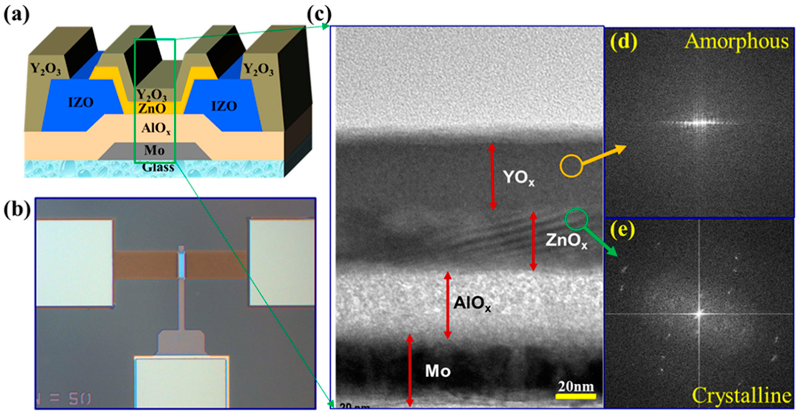
2.2. Device Fabrication

We fabricate the bottom-gate, bottom-contact (BG-BC) ZnO TFT while using Al2O3 as a GI. Figure 1a shows the cross-sectional view of BG-BC ZnO TFT and Figure 1b shows the optical image of the TFT after fabrication with the channel width and length of 50 μm and 10 μm, respectively. A 40 nm thick molybdenum (Mo) layer was deposited on a glass substrate by DC sputtering. The Mo film was patterned and etched for the gate electrode by photolithography. Subsequently, Aluminum oxide (Al2O3) thin film was deposited on the patterned Mo backplane by spin coating at 2000 rpm for 30 s. Afterwards, the film was cured on hot plate (250 °C) for 5 min. and exposed under UV lamp (A low-pressure mercury lamp was used as light source having wavelengths of 185 & 254 nm.) at 100 °C for UV/O3 treatment for 5 min. The process was repeated twice to obtain the thickness of ~40 nm, and then annealed in a furnace at 350 °C for two hours. Subsequently, the Al2O3 film was patterned by photolithography and wet etched for via-holes. A 100 nm thick Indium-zinc-oxide (IZO) layer was deposited by direct current (DC) sputtering and then patterned for the source/drain (S/D) electrodes while using conventional photolithography. A 25 nm of ZnO semiconductor was deposited by spray pyrolysis at the substrate temperature of 350 °C [12]. The movement of nozzle was controlled horizontally and vertically for n uniform film. The distance between the spray nozzle and the substrate maintained about 8 cm. The flow rate of precursor solution was 3 mL/min. and each spray cycle over 15 cm × 15 cm substrate is 60 s. The film was deposited at 350 °C and the process was repeated five times to get the 25 nm thick ZnO film. The ZnO layer was patterned by photolithography and wet etched for the active island. The channel width and length of TFTs are 50 and 10 μm, respectively. Finally, the YOx film with thickness of 35 nm was deposited at 400 °C by spray pyrolysis as a passivation layer. YOx film was deposited using the same flow rate of the precursor solution and then patterned using photolithography.

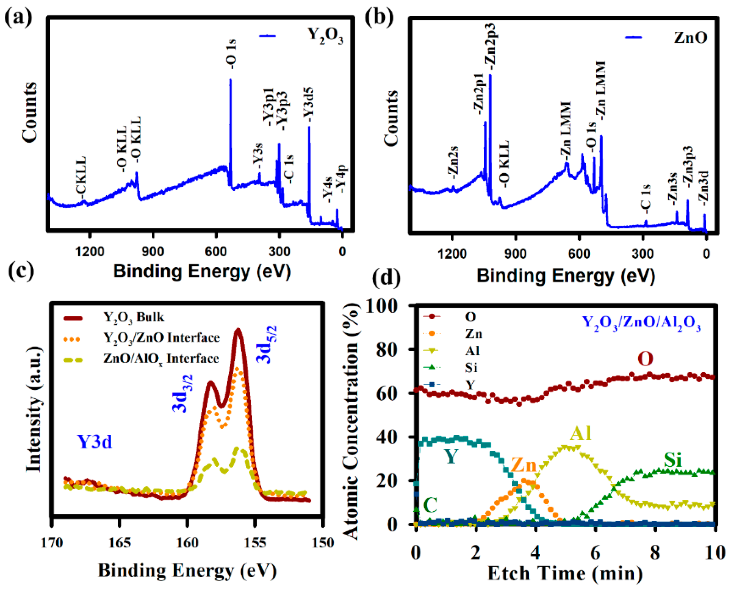
2.3. Characterization Techniques

We characterized the ZnO and YOx films by the scanning electron microscopy (SEM), X-ray diffraction (XRD), X-ray photoelectron spectroscopy (XPS), and scanning transmission electron microscope (STEM). The electrical properties of TFTs were measured using Agilent 4156C semiconductor parameter analyzer (Hewlett-Packard, Seoul, South Korea). The transfer curves were measured with the drain voltage (VDS) of 0.1 V and the gate voltage (VGS) was swept from −5 to +5 V. In the saturation region (VDS ≥ VGS − VTH), the mobility was calculated using the equation IDS = (W/2L) μsat Ci (VGS − VTH)2, where IDS, VGS, μsat, W, L, VTH, and Ci are the drain current, gate voltage, saturation mobility, channel width, channel length, threshold voltage, and gate insulator capacitance, respectively. The VTH was determined from the intercept of x-axis from √(IDS) versus VGS plot by linear extrapolation and the saturation mobility (μsat) from the slope of the linear part of the curve. The subthreshold swing (SS) was obtained from the equation SS = dVGS/d(log IDS) over the current range of 10 pA ≤ IDS ≤ 100 pA with VDS = 0.1 V.

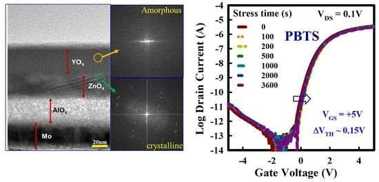
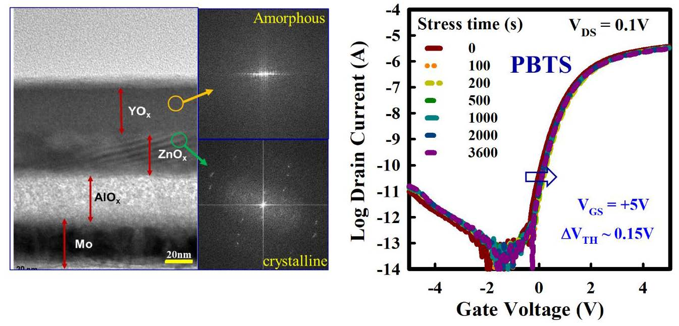
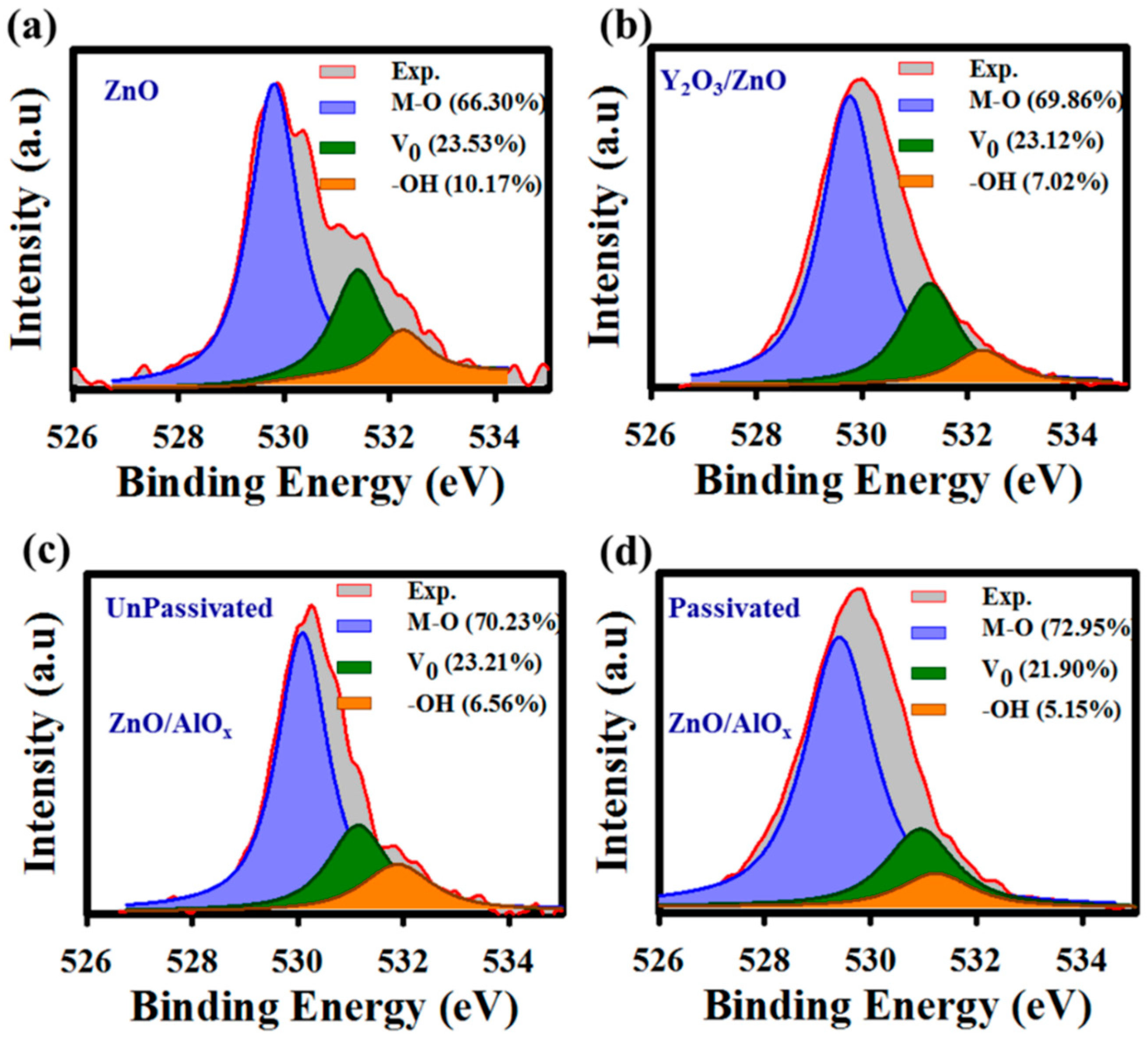
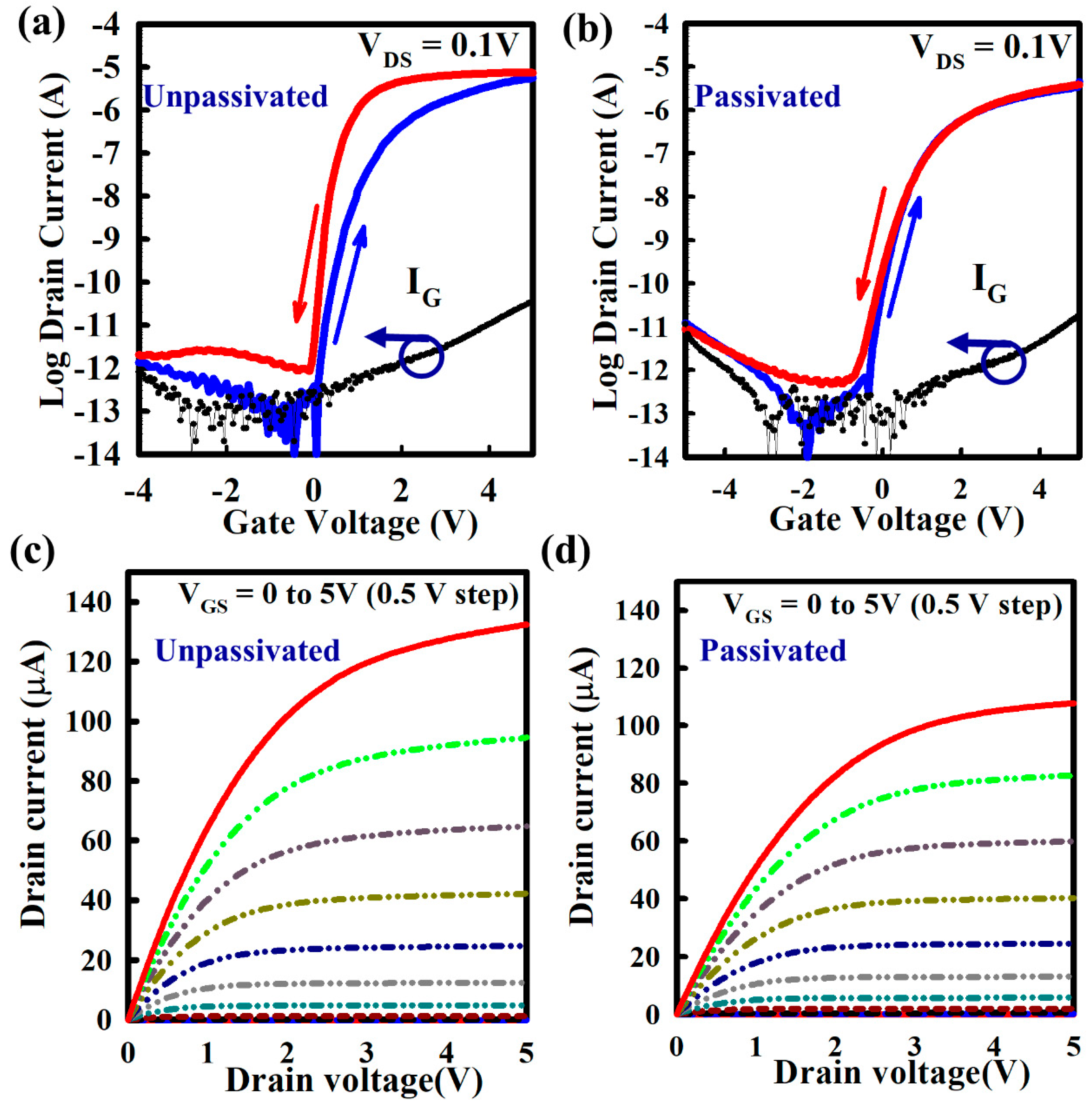
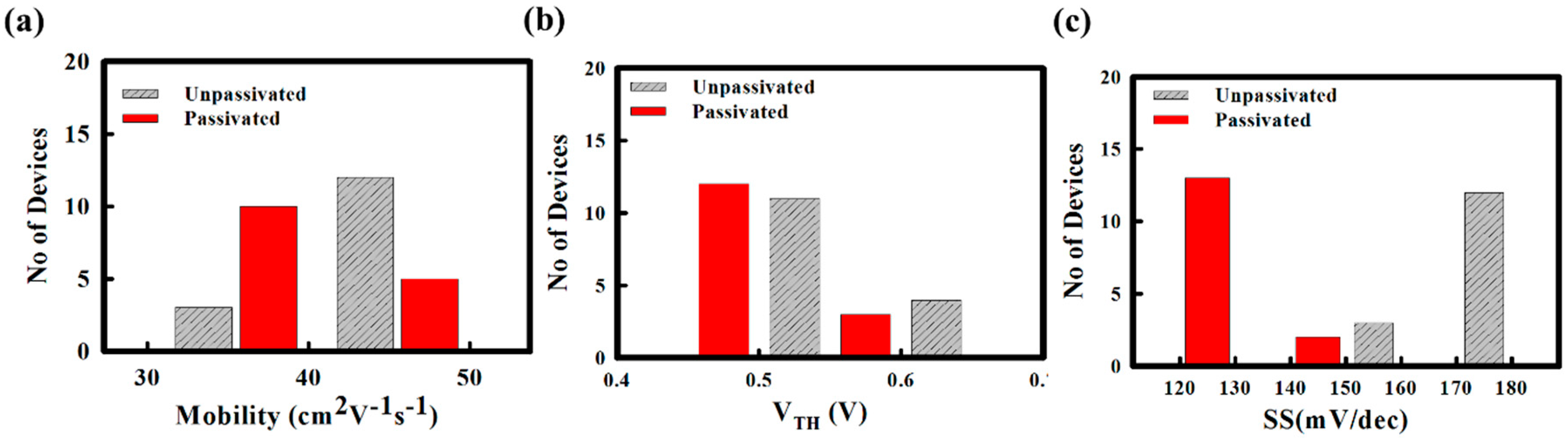
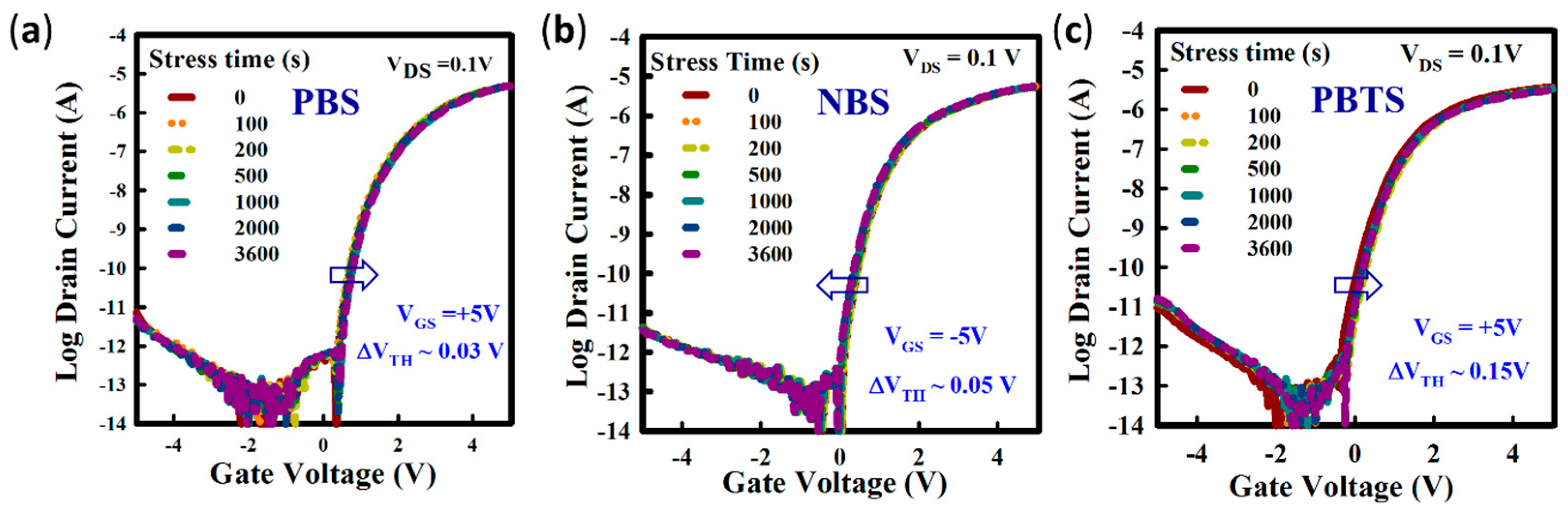
3. Results and Discussions

Figure 1c shows the scanning transmission electron microscopy (STEM) image of the Y2O3/ZnO/Al2O3/Mo layers in a TFT. The image reveals uniform and continuous Y2O3/ZnO/ Al2O3/Mo interface. The thicknesses of ZnO and Y2O3 are ~25 and ~35 nm, respectively. Figure 1d,e show the fast Fourier transform (FFT) patterns for the areas indicated by the yellow circle for Y2O3 and green circle for ZnO, which reveal the nano-crystalline structure of ZnO and amorphous structure of Y2O3,, respectively. In addition, we confirmed the nanocrystalline structure of ZnO and amorphous structure of Y2O3 by XRD as shown in Figure S1. The XRD spectrum shows three strong peaks corresponding to (100), (002), and (101) planes, with the most preferred orientation being (002) plane of the hexagonal wurtzite structure. On the other hand, the Y2O3 film has no XRD peak because of amorphous phase. Figure S2 shows the SEM of the ZnO and Y2O3 surface, where we can see the ZnO film are nano-crystalline with grain size of 30 nm. The ZnO film shows dense and uniform distribution of grains, which are advantageous to the electron transport. The surface morphologies of Al2O3 and ZnO thin films were studied by atomic force microscopy (AFM) measurement (Scale: 5 μm × 5 μm). Figure S3a shows the surface morphology of Al2O3 thin film with root means square (RMS) roughness of 0.16 nm, whereas Figure S3b shows the Rrms of ZnO of 1.28 nm. Therefore, the smooth surfaces of both ZnO and Al2O3 thin films are good for carrier transport [22]. In both cases of films, such as dense and uniform distribution of grains, including smooth surface, leads to lower density of defects (charge traps and recombination centers).
X-ray photoelectron spectroscopy (XPS) analysis reveals the chemical binding states of the elements and their distributions in the film. The energy of an X-ray used in XPS with particular wavelength (beam of monochromatic Al Kα X-rays, Ephoton = 1486.7 eV). Figure 2a,b show wide-scan spectra (on the surface) of ZnO film and Y2O3 passivation layers. At the surface of the ZnO film, the peaks of Zn2p and O1s confirm ZnO formation. The presence of Y3d and O1s at the surface of YOx film confirms the formation of Y2O3. The Y3d binding energy peak shows two splitting orbitals Y3d5/2 and Y3d3/2 positioned at 156.5 and 158.7 eV, respectively, as shown in Figure 2c. This confirms the formation of Y2O3 [21]. The atomic percentages of C, O, Zn, Al, and Y at the surface of ZnO without Y2O3 are 18, 42, 40, 0, and 0%, respectively. Whereas, the atomic percentages are 12.45, 63, 0, 0, and 24.55% at the surface of Y2O3, respectively [20].
The presence of carbon usually acts as carrier recombination centers. The percentage of C high only at the surface not in the bulk. Carbon is the material, which always present in atmosphere, so nano level layer is deposited on the samples. In general, the properties of carrier transport for ZnO semiconductor are closely related to the chemical states of ZnO thin film, such as a metal-oxygen bond (M–O), oxygen vacancies (Vo), and hydroxyl groups (–OH). XPS depth analysis was carried out for ZnO/Al2O3 without and with Y2O3 passivation to explore the chemical states of ZnO thin film and its interface with the GI. From the depth profile, the formation of individual layers of Y2O3, ZnO, and Al2O3 are confirmed, as shown in Figure 2d. The presence of Y at the interface of Y2O3/ZnO, in bulk ZnO and the interface of ZnO/Al2O3 confirm the diffusion of Y to ZnO until GI. This passivates the defects at the interface [19,20,21].
Through the Gaussian–Lorentzian fitting method, the O 1s intensity peak is deconvoluted into three peaks at 530 eV, 531 eV, and 532 eV, corresponding to M–O, Vo and M–OH, respectively. The O1s deconvolution on the surface of ZnO is shown in Figure 3a, where the M–O bonding is 66.30% and the defects (oxygen vacancy and –OH group) are 33.70% (23.53% and 10.17%) for the unpassivated ZnO. Whereas, the passivated ZnO shows the increase of M-O bonding and reduction of defects on Y2O3/ZnO, as shown in Figure 3b. M–O bonding and defects at the interface of Y2O3/ZnO are 69.86% and 30.14%, respectively. The O1s deconvolution at the ZnO/Al2O3 interface without and with Y2O3 passivation are shown, respectively, in Figure 3c,d. The M–O bonds increase from 70.23 to 72.95% and the defects (oxygen vacancy and –OH group) decrease from 29.77 to 27.05% by Y2O3 passivation. The improvements in the ZnO and ZnO/Al2O3 interface are due to the diffusion of Y at the bulk of ZnO as well as at the ZnO/Al2O3 interface [20,21]. Even a slight change in film composition by higher bond dissociation energy, such as Y–O (714.1 ± 10.2 kJ/mol), can enhance the electrical properties [20,21].
Figure 4a,b show the transfer characteristics of ZnO TFT without and with Y2O3 passivation, respectively. The transfer curve with hysteresis characteristics and gate leakage currents are shown as a function of VGS. The electrical properties of unpassivated ZnO TFT are the μFE of 42.66 cm2V−1s−1, VTH of 0.58 V, and SS of 172.40 mV/dec, whereas passivated ZnO TFT exhibits the μFE of 35.36 cm2V−1s−1, VTH of 0.49 V, and SS of 128.40 mV/dec. The anti-clockwise hysteresis for the unpassivated ZnO TFT implies for the electron detrapping from high-k gate dielectrics at the interface between gate insulator and active layer, which generate extra carriers in the channel at negative gate bias [23]. After Y2O3 passivation, the defects at the ZnO/Al2O3 interface has reduced due to Y diffusion, which reduces the trapping and detrapping of carriers and provides a negligible hysteresis. The output curves of ZnO TFT without and with passivation are shown, respectively, in Figure 4c,d. The output curves are showing clear pinch-off and saturation behavior. There are no current crowding in the linear region, indicating the excellent ohmic contact between active layer and S/D. The reduction of mobility with zero hysteresis voltage is most probably due to the excess amount of Y (around 10%, as highlighted by XPS depth analysis), which can suppress the carrier concentration, thus reducing mobility [24]. The interface state density NSS, as calculated from SS for unpassivated and passivated ZnO TFTs, are 2.69 × 10¹² and 7.38 × 1011 cm−2eV−1, respectively. Table 1 shows the summary of device performances, such as μFE, SS, and ION/IOFF, including the data from the literatures [19,20,21,25,26,27,28,29].
Among all reports, our spray pyrolyzed Y2O3 passivated ZnO TFT shows superior mobility. The higher mobility with good stability is due to the interface quality between gate insulator and semiconductor layer, which has further confirmed from the TEM image and XPS analysis. We measured 15 TFTs with same W/L (50 μm/10 μm) at different locations to check the uniformity of spray coated TFTs at different position over 7.5 cm × 7.5 cm substrate glass. The histograms show the comparison of μFE, VTH, and SS values for ZnO TFTs without and with Y2O3 passivation, as shown in Figure 5a–c. The average μFE for unpassivated and passivated ZnO TFTs are 43.13 ± 3.48 and 36.88 ± 3.75 cm2/V.s, respectively. The average VTH for unpassivated and passivated ZnO TFTs are 0.61 ± 0.05 and 0.50 ± 0.04 V, respectively. In addition, the average SS for unpassivated and passivated ZnO TFTs are 170.40 ± 9.22 and 126.40 ± 10.98 mV/dec, respectively. Table 2 summarizes electrical performances of ZnO TFT fabricated by spray pyrolysis without and with Y2O3 passivation and statistical data for 15 ZnO TFTs.
For the electrical stability of the spray coated ZnO TFTs without and with Y2O3 passivation, the positive bias stress (PBS) at VGS of +5 V and negative bias stress (NBS) at VGS of −5 V were applied by varying the stress time from 0 to 1 h. Figure 6a,b show the evolution of transfer curves under PBS and NBS were measured by sweeping gate voltage from −5 to +5 V at the same drain voltage (VDS) of 0.1V for passivated ZnO TFT.
Additionally, Figure S4a,b show the evolution of transfer curves under PBS and NBS for unpassivated ZnO TFT. The ∆VTH for unpassivated ZnO TFT under PBS and NBS are 0.3 and 0.25 V, respectively, whereas the Y2O3 passivated ZnO TFT shows the ∆VTH values of 0.03 and 0.05 V, respectively. The positive shift of the transfer curve is understood by the trapping of electrons at the ZnO/Al2O3 interface [30,31]. Small ∆VTH indicates fewer defects at the interface of the GI and the active layer. The negligible change in the SS after bias stress from 0 to 1 h indicates very small trapping sites at the interface [32,33].
The positive-bias-temperature-stress (PBTS) (at VGS = 5 V for 1 h) for the ZnO TFT was investigated. Figure 6c shows the evolution of transfer curves of the ZnO TFT under PBTS for 1 h in dark at 60 °C, as measured by sweeping VGS from −5 to +5 V at a VDS of 0.1 V. The positive ∆VTH (0.78 V) is due to the electron trapping at the ZnO/Al2O3 interface for unpassivated ZnO TFT, as shown in Figure S5. The Y2O3 passivated ZnO TFT is highly stable under PBTS for 1 h in dark showing ∆VTH of 0.15 V [34,35,36,37]. Therefore, the improvement in the operational stability is due to the significant reduction of ZnO/Al2O3 interface trap by interfacial defects. Furthermore, we also checked the long-term stability of Y2O3 passivated ZnO TFT in ambient air for six months and measured the TFT performance after a certain interval. There is no significant change observed in the performance of ZnO TFT with Y2O3 passivation shown in Figure S6. Therefore, the spray coated Y2O3 passivation layer at 400 °C is quite good to protect the device from the absorption or desorption of oxygen present in air.

4. Conclusions

We studied the impact of yttrium oxide (Y2O3) passivation layer on the performance of zinc oxide (ZnO) thin film transistor (TFT) based on Al2O3 gate insulator (GI). Y2O3 and ZnO films are both deposited by spray pyrolysis at 400 and 350 °C, respectively. Y2O3 passivated ZnO TFT exhibits field effect mobility (μFE) of 35.36 cm2/Vs, threshold voltage (VTH) of 0.49 V, subthreshold swing (SS) of 128.4 mV/dec., and hysteresis voltage (VH) of ~0 V. The negligible threshold voltage shift (∆VTH) of 0.15 V under positive bias temperature stress (PBTS) was found in the passivated device. The yttrium (Y) can improve the device performance due to its higher bond dissociation energy with oxygen. It can also protect the channel from moisture absorption. In addition, the diffusion of Y until the ZnO/Al2O3 interface reduces the interfacial defects. The Y diffusion, as confirmed from the XPS analysis, leads to the decrease of oxygen related defects and to increasing the M-O-M bond network at the ZnO/Al2O3 interface. Therefore, the solution-processed Y2O3 passivation on metal oxide TFTs is a good approach for next-generation display technology.

Supplementary Materials

The following are available online at https://www.mdpi.com/2079-4991/10/5/976/s1. Figure S1: XRD spectra of (a) ZnO film deposited at 350 °C, and (b) Y2O3 film deposited at 400 °C, Figure S2: SEM image of (a) nano-crystalline ZnO film (b) amorphous Y2O3 film, Figure S3: AFM image for surface roughness of spray coated (a) nano-crystalline ZnO film, and (b) amorphous Al2O3 film, Figure S4: The evolution of transfer curve under bias stress for ZnO TFT without Y2O3 passivation. Transfer curves of ZnO TFTs under (a) PBS, and (b) NBS. Figure S5: The evolution of transfer curve under positive bias temperature stress for ZnO TFT without Y2O3 passivation. Figure S6: The evolution of transfer curve of Y2O3 passivated ZnO TFT in ambient air for long-term stability.

Author Contributions

All authors contributed to this work equally. All authors have read and agreed to the published version of the manuscript.

Funding

This work supported by the Technology Innovation Program (or) Industrial Strategic Technology Development Program (10080454, Development of High-resolutions OLED Micro-Display and Controller SoC for AR/VR Device) funded by the Ministry of Trade, Industry & Energy (MOTIE, Korea).

Acknowledgments

We are thankful to Advanced Display Research Center, Department of Information Display, Kyung-Hee University to support for using equipment’s for the experiments.

Conflicts of Interest

The authors declare no conflict of interest.

References

  1. Song, K.; Noh, J.; Jun, T.; Jung, Y.; Kang, H.Y.; Moon, J. Fully Flexible Solution-Deposited ZnO Thin-Film Transistors. Adv. Mater. 2010, 22, 4308–4312. [Google Scholar] [CrossRef] [PubMed]
  2. Kwon, J.Y.; Jeong, J.K. Recent progress in high performance and reliable n-type transition metal oxide-based thin film transistors. Semicond. Sci. Technol. 2015, 30, 024002. [Google Scholar] [CrossRef]
  3. Gleskova, H.; Wagner, S. Electron mobility in amorphous silicon thin-film transistors under compressive strain. Appl. Phys. Lett. 2001, 79, 3347–3349. [Google Scholar] [CrossRef]
  4. Fortunato, E.; Pimentel, A.; Pereira, L.; Goncalves, A.; Lavareda, G.; Aguas, H.; Ferreira, I.; Carvalho, C.N.; Martins, R. High field-effect mobility zinc oxide thin film transistors produced at room temperature. J. Non Cryst. Solids 2004, 338, 806–809. [Google Scholar] [CrossRef]
  5. Adamopoulos, G.; Bashir, A.; Gillin, W.P.; Georgakopoulos, S.; Shkunov, M.; Baklar, M.A.; Stingelin, N.; Bradley, D.D.C.; Anthopoulos, T.D. Structural and Electrical Characterization of ZnO Films Grown by Spray Pyrolysis and Their Application in Thin-Film Transistors. Adv. Funct. Mater. 2011, 21, 525–531. [Google Scholar] [CrossRef]
  6. Hirao, T.; Furuta, M.; Hiramatsu, T.; Matsuda, T.; Li, C.; Furuta, H.; Hokari, H.; Yoshida, M.; Ishii, H.; Kakegawa, M. Bottom-Gate Zinc Oxide Thin-Film Transistors for AMLCDs. IEEE Trans. Electron Devices. 2008, 55, 3136–3142. [Google Scholar] [CrossRef]
  7. Isakov, I.; Faber, H.; Grell, M.; Moon, G.W.; Pliatsikas, N.; Kehagias, T.; Dimitrakopulos, G.P.; Patsalas, P.P.; Li, R.; Anthopoulos, T.D. Exploring the Leidenfrost Effect for the Deposition of High-Quality In2O3 Layers via Spray Pyrolysis at Low Temperatures and Their Application in High Electron Mobility Transistors. Adv. Funct. Mater. 2007, 27, 1606407. [Google Scholar] [CrossRef]
  8. Jun, T.; Jung, Y.; Song, K.; Moon, J. Influences of pH and Ligand Type on the Performance of Inorganic Aqueous Precursor-Derived ZnO Thin Film Transistors. ACS Appl. Mater. Interfaces 2011, 3, 774–781. [Google Scholar] [CrossRef]
  9. Cho, S.W.; Yun, M.G.; Ahn, C.H.; Kim, S.H.; Cho, H.K. Bilayer Channel Structure-Based Oxide Thin-Film Transistors Consisting of ZnO and Al-Doped ZnO with Different Al Compositions and Stacking Sequences. Electron. Mater. Lett. 2015, 11, 198–205. [Google Scholar] [CrossRef]
  10. Park, J.; Huh, J.E.; Lee, S.E.; Lee, J.; Lee, W.H.; Lim, K.H.; Kim, Y.S. Effective atmospheric-pressure plasma treatment toward high performance solution-processed oxide thin-film transistors. ACS Appl. Mater. Interfaces 2018, 10, 30581–30586. [Google Scholar] [CrossRef]
  11. Levy, D.H.; Freeman, D.; Nelson, S.F.; Corvan, P.J.C.; Irving, L.M. Stable ZnO thin film transistors by fast open air atomic layer deposition. Appl. Phys. Lett. 2008, 92, 2101. [Google Scholar] [CrossRef]
  12. Kim, Y.; Avis, C.; Hwang, H.R.; Kim, T.W.; Seol, Y.G.; Jang, J. Effect of Strontium Addition on Stability of Zinc-Tin-Oxide Thin-Film Transistors Fabricated by Solution Process. J. Display Technol. 2014, 10, 939–944. [Google Scholar] [CrossRef]
  13. Saha, J.K.; Billah, M.M.; Bukke, R.N.; Kim, Y.G.; Mude, N.N.; Siddik, A.B.; Islam, M.M.; Do, Y.; Choi, M.; Jang, J. Highly Stable, Nanocrystalline, ZnO Thin-Film Transistor by Spray Pyrolysis Using High-k Dielectric. IEEE Trans. Electron Devices 2020, 67, 1021–1026. [Google Scholar] [CrossRef]
  14. Branquinho, R.; Salgueiro, D.; Santa, A.; Kiazadeh, A.; Barquinha, P.; Pereira, L.; Martins, R.; Fortunato, E. Towards environmental friendly solution-based ZTO/AlOx TFTs. Semicond. Sci. Technol. 2015, 30, 024007. [Google Scholar] [CrossRef]
  15. Zhang, L.; Zhang, H.; Bai, Y.; Ma, J.W.; Cao, J.; Jiang, X.; Zhang, Z.L. Enhanced performances of ZnO-TFT by improving surface properties of channel layer. Solid State Commun. 2008, 146, 387–390. [Google Scholar] [CrossRef]
  16. Bashir, A.; Wöbkenberg, P.H.; Smith, J.; Ball, J.M.; Adamopoulos, G.; Bradley, D.D.C.; Anthopoulos, T.D. High-Performance Zinc Oxide Transistors and Circuits Fabricated by Spray Pyrolysis in Ambient Atmosphere. Adv. Mater. 2009, 21, 2226–2231. [Google Scholar] [CrossRef]
  17. Kim, D.H.; Yoon, S.B.; Jeong, Y.T.; Kim, Y.M.; Kim, B.S.; Hong, M.P. Role of adsorbed H2O on transfer characteristics of solution-processed zinc tin oxide thin-film transistors. Appl. Phys. Express 2012, 5, 021101. [Google Scholar] [CrossRef]
  18. Xu, X.; Cui, Q.; Jin, Y.; Guo, X. Low-voltage zinc oxide thin-film transistors with solution-processed channel and dielectric layers below 150 °C. Appl. Phys. Lett. 2012, 101, 2114–2116. [Google Scholar] [CrossRef]
  19. An, S.; Mativenga, M.; Kim, Y.; Jang, J. Improvement of bias-stability in amorphous-indium-gallium-zinc-oxide thin-film transistors by using solution-processed Y2O3 passivation. Appl. Phys. Lett. 2014, 105, 053507–053511. [Google Scholar] [CrossRef]
  20. Bukke, R.N.; Avis, C.; Jang, J. Solution-Processed Amorphous In–Zn–Sn Oxide Thin-Film Transistor Performance Improvement by Solution-Processed Y2O3 Passivation. IEEE Electron Device Lett. 2016, 37, 433–436. [Google Scholar] [CrossRef]
  21. Lee, S.H.; Kim, T.; Lee, J.; Avis, C.; Jang, J. Solution-Processed Gadolinium Doped Indium-Oxide Thin-Film Transistors with Oxide Passivation. Appl. Phys. Lett. 2017, 110, 122102. [Google Scholar] [CrossRef]
  22. Guo, X.; Silva, S.R.P.; Ishii, T. Current percolation in ultrathin channel nano-crystalline silicon transistors. Appl. Phys. Lett. 2008, 93, 042105. [Google Scholar] [CrossRef] [Green Version]
  23. Lin, H.C.; Hung, C.H.; Chen, W.C.; Lin, Z.M.; Hsu, H.H.; Hunag, T.Y. Origin of hysteresis in current-voltage characteristics of polycrystalline silicon thin-film transistors. J. Appl. Phys. 2009, 105, 054502. [Google Scholar] [CrossRef] [Green Version]
  24. Abliz, A.; Xu, L.; Wan, D.; Duan, H.; Wang, J.; Wang, C.; Luo, S.; Liu, C. Effects of yttrium doping on the electrical performances and stability of ZnO thin-film transistors. Appl. Surf. Sci. 2019, 475, 565–570. [Google Scholar] [CrossRef]
  25. Kim, J.H.; Rim, Y.H.; Kim, H.J. Homojunction Solution-Processed Metal Oxide Thin-Film Transistors Using Passivation-Induced Channel Definition. ACS Appl. Mater. Interfaces 2014, 6, 4819–4822. [Google Scholar] [CrossRef]
  26. Xu, X.; Feng, L.; He, S.; Jin, Y.; Guo, X. Solution-Processed Zinc Oxide Thin-Film Transistors with a Low-Temperature Polymer Passivation Laye. IEEE Electron Device Lett. 2012, 33, 1420–1422. [Google Scholar] [CrossRef]
  27. Nomura, K.; Kamiya, T.; Hosono, H. Stability and high-frequency operation of amorphous In–Ga–Zn–O thin-film transistors with various passivation layers. Thin Solid Films 2012, 520, 3778–3782. [Google Scholar] [CrossRef]
  28. Wan, L.; He, F.; Qin, Y.; Lin, Z.; Su, J.; Chang, J.; Hao, Y. Effects of Interfacial Passivation on the Electrical Performance, Stability, and Contact Properties of Solution Process Based ZnO Thin Film Transistors. Materials 2018, 11, 1761. [Google Scholar] [CrossRef] [Green Version]
  29. Hong, S.; Park, S.P.; Kim, Y.G.; Kang, B.H.; Na, J.W.; Kim, H.J. Low-temperature fabrication of an HfO2 passivation layer for amorphous indium-gallium-zinc oxide thin film transistors using a solution process. Sci. Rep. 2017, 7, 16265. [Google Scholar] [CrossRef] [Green Version]
  30. Zhou, Y.; Dong, C. Influence of passivation layers on positive gate bias-stress stability of amorphous InGaZnO thin-film transistors. Micromachines 2018, 9, 603. [Google Scholar] [CrossRef] [Green Version]
  31. Xiao, P.; Wang, W.; Ye, Y.; Dong, T.; Yuan, S.; Deng, J.; Zhang, L.; Chen, J.; Yuan, J. Back-Channel-Etched InGaZnO Thin-Film Transistors with Au Nanoparticles on the Back Channel Surface. Electron. Mater. Lett. 2020, 16, 115–122. [Google Scholar] [CrossRef]
  32. Shaw, A.; Wrench, J.S.; Jin, J.D.; Whittles, T.J.; Mitrovic, I.Z.; Raja, M.; Dhanak, V.R.; Chalker, P.R.; Hall, S. Atomic layer deposition of Nb-doped ZnO for thin film transistors. Appl. Phys. Lett. 2016, 109, 222103. [Google Scholar] [CrossRef] [Green Version]
  33. Mude, N.N.; Bukke, R.N.; Saha, J.K.; Avis, C.; Jang, J. Highly Stable, Solution Processed Ga Doped IZTO Thin Film Transistor by Ar/O2 Plasma Treatment. Adv. Electron. Mater. 2019, 6, 1900768. [Google Scholar] [CrossRef]
  34. Afouxenidis, D.; Mazzocco, R.; Vourlias, G.; Livesley, P.J.; Krier, A.; Milne, W.I.; Kolosov, O.; Adamopoulos, G. ZnO-based Thin Film Transistors Employing Aluminum Titanate Gate Dielectrics Deposited by Spray Pyrolysis at Ambient Air. ACS Appl. Mater. Interfaces 2015, 7, 7334. [Google Scholar] [CrossRef]
  35. Yang, J.; Zhang, Y.; Qin, C.; Ding, X.; Zhang, J. Low-Voltage Hf-ZnO Thin Film Transistors with Ag Nanowires Gate Electrode and Their Application in Logic Circuit. IEEE Trans. Elec. Dev. 2019, 66, 1760. [Google Scholar] [CrossRef]
  36. Kim, D.N.; Kim, D.L.; Kim, G.H.; Kim, S.J.; Rim, Y.S.; Jeong, W.H.; Kim, H.J. The effect of La in InZnO systems for solution-processed amorphous oxide thin-film transistors. Appl. Phys. Lett. 2010, 97, 192105. [Google Scholar] [CrossRef]
  37. Zhang, L.; Li, J.; Zhang, X.; Jiang, X.; Zhang, Z. High performance ZnO-thin-film transistor with TaO5 dielectrics fabricated at room temperature. Appl. Phys. Lett. 2009, 95, 072112–072114. [Google Scholar] [CrossRef]
Figure 1. (a) Schematic diagram and (b) optical image of the bottom gate bottom contact ZnO TFT with Y2O3 passivation by spray pyrolysis. (c) Cross-sectional transmission electron microscope (TEM) image of a ZnO TFT. Fast Fourier Transform (FFT) of (d) yellow circled area confirms the amorphous nature of Y2O3 layer deposited at 400 °C and (e) green circled area confirms the hexagonal structured ZnO deposited at 350 °C by spray pyrolysis.
Nanomaterials 10 00976 g001
Figure 2. X-ray photoelectron spectroscopy (XPS) survey spectra of (a) Y2O3 and (b) ZnO films. (c) The Y3d peaks at different depths of Y2O3/ZnO/Al2O3 film. Y could be found at the bottom interface (ZnO/Al2O3). (d) XPS depth profiles of O, Y, C, Zn, Al, and Si of Y2O3/ZnO/Al2O3 film.
Nanomaterials 10 00976 g002
Figure 3. XPS spectra analysis of the deconvoluted O 1s peak (a) in the bulk of ZnO and (b) at the interface of Y2O3/ZnO. Deconvoluted O 1s peak at the interface of ZnO/Al2O3 (c) without and (d) with Y2O3 passivation. The individual contribution of metal oxide (M–O), oxygen vacancy (Vo) and metal hydroxyl group (M–OH) are shown by area under the blue line (~529.5 eV), green line (~531 eV), and orange line (~532 eV), respectively. After Y2O3 passivation the Vo and –OH concentrations are reduced at the interface of Y2O3/ZnO as well as interface of ZnO/Al2O3.
Nanomaterials 10 00976 g003
Figure 4. Electrical performance of ZnO TFT without and with Y2O3 passivation by spray pyrolysis. (a,b) Plots of the transfer characteristics with hysteresis and gate leakage currents (IG) as a function of VGS for (a) without and (b) with Y2O3 passivation. (c,d) Output curves of ZnO (c) without and (d) with Y2O3 passivation. The hysteresis voltage of the thin film transistor (TFT) was taken at IDS = 10−10 A with forward sweep from −5 to +5 V and reverse sweep from +5 to −5 V at the same drain voltage (VDS = 0.1 V). Output curves were measured by varying VGS from 0 to +5 V with a 0.5 V step.
Nanomaterials 10 00976 g004
Figure 5. Statistical analysis of the electrical performances of the ZnO TFTs without and with Y2O3 passivation. The histogram of 15 ZnO TFTs for (a) mobility, (b) VTH, and (c) subthreshold swing (SS), respectively.
Nanomaterials 10 00976 g005
Figure 6. The evolution of transfer curve under bias stress for the ZnO TFTs with Y2O3 passivation. Transfer curves of ZnO TFTs under (a) positive bias stress (PBS), (b) negative bias stress (NBS), and (c) positive-bias-temperature-stress (PBTS) at 60 °C. Thetransfer curve of the TFT measured by sweeping VGS from −5 to +5 V at the drain voltage, VDS = 0.1 V for 1 h.
Nanomaterials 10 00976 g006
Table 1. The summary of processing methods and electrical performances (field effect mobility, subthreshold swing, and current on/off ratio) of the solution processed oxide TFTs with various passivation layers.
Active/GIPassivation LayerProcessing MethodSubstrate Temp. (°C)μFE [cm2V−1s−1]SS [mV/dec]Ion/IoffYear
InOx/SiO2AlOxSC4000.027301062014 (25)
ZnO/SiOxPDMSSC1500.502401062012 (26)
IGZO/SiO2Y2O3SC25021.311601082014 (19)
IZTO/ZrOxY2O3SC3504.751141092016 (20)
IGZO/SiO2Y2O3SC35011.101401082012 (27)
GdInOx/AlOxY2O3SC3509.47791072017 (21)
ZnO/SiO2PCBASC1504.50-1062018 (28)
IGZO/SiO2HfOxSC2509.603501082017 (29)
IGZO/SiO2Y2O3SC25011.302671032017 (29)
IGZO/SiO2PMMASC2509.513201082017 (29)
ZnO/AlOxY2O3SP35035.36128108This work
GI: Gate Insulator, SC: Spin Coating, SP: Spray Coating, Temp.: temperature
Table 2. Summary of the electrical performances of 15 ZnO TFTs fabricated by spray pyrolysis without and with Y2O3 passivation.
ZnO TFTµFE (cm2V−1 s−1)Vth (V)SS (mV/dec)
Without passivation43.13 ± 3.480.61 ± 0.05170.40 ± 9.22
With passivation36.88 ± 3.750.50 ± 0.04126.40 ± 10.98

