Comparative Study of the Structure, Composition, and Electrocatalytic Performance of Hydrogen Evolution in MoSx~2+δ/Mo and MoSx~3+δ Films Obtained by Pulsed Laser Deposition


Abstract
1. Introduction
2. Materials and Methods
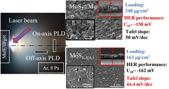
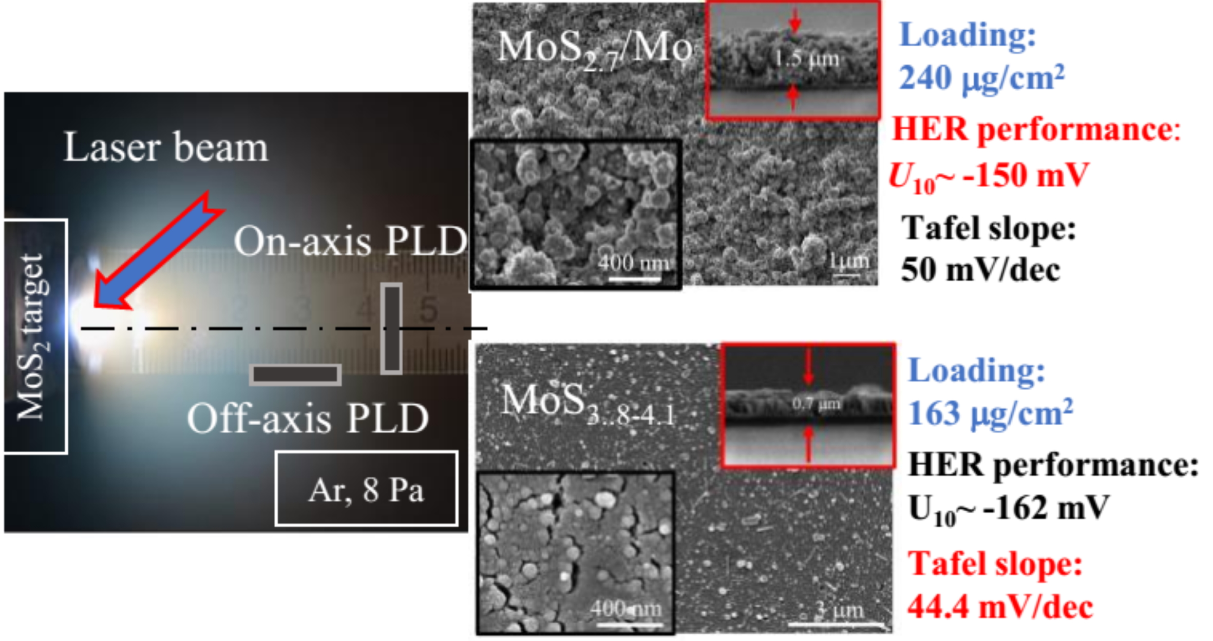
2.1. Experimental Methods for the on- and off-Axis PLD of MoSx Films
2.2. Structural and Electrochemical Characterization of the Prepared MoSx Films
3. Results
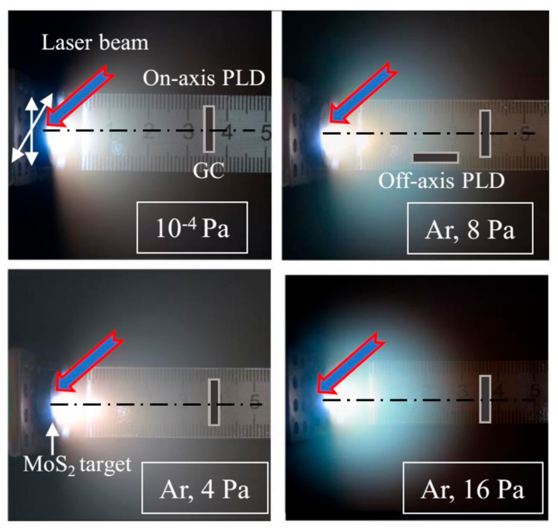
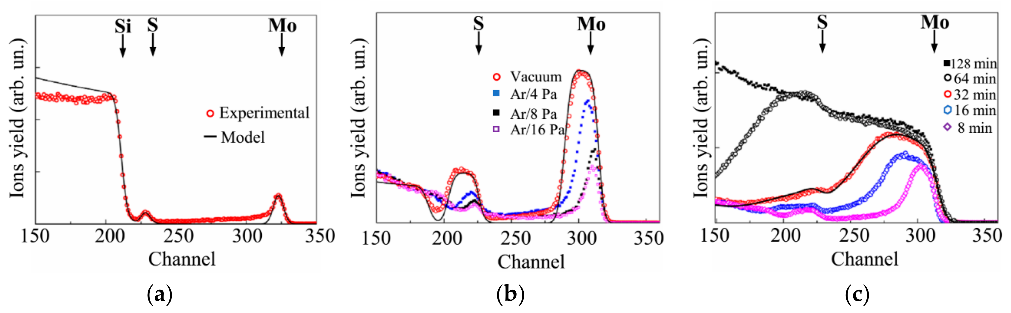
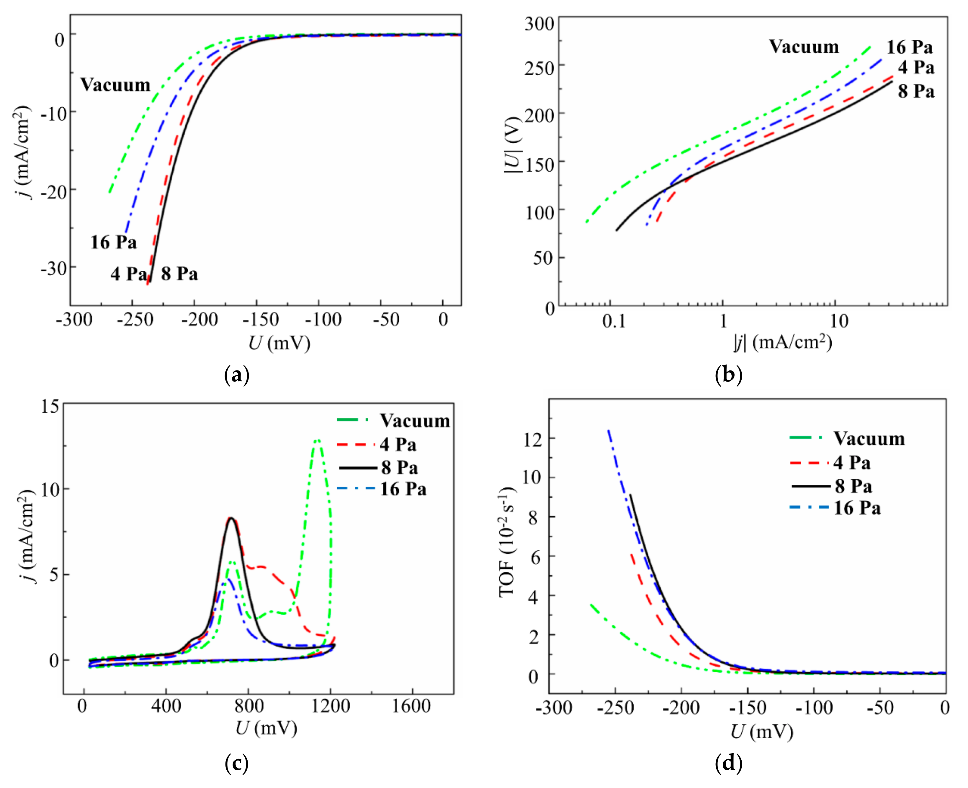
3.1. Selection of the Conditions (Buffer Gas Pressure) for the PLD of MoSx Films
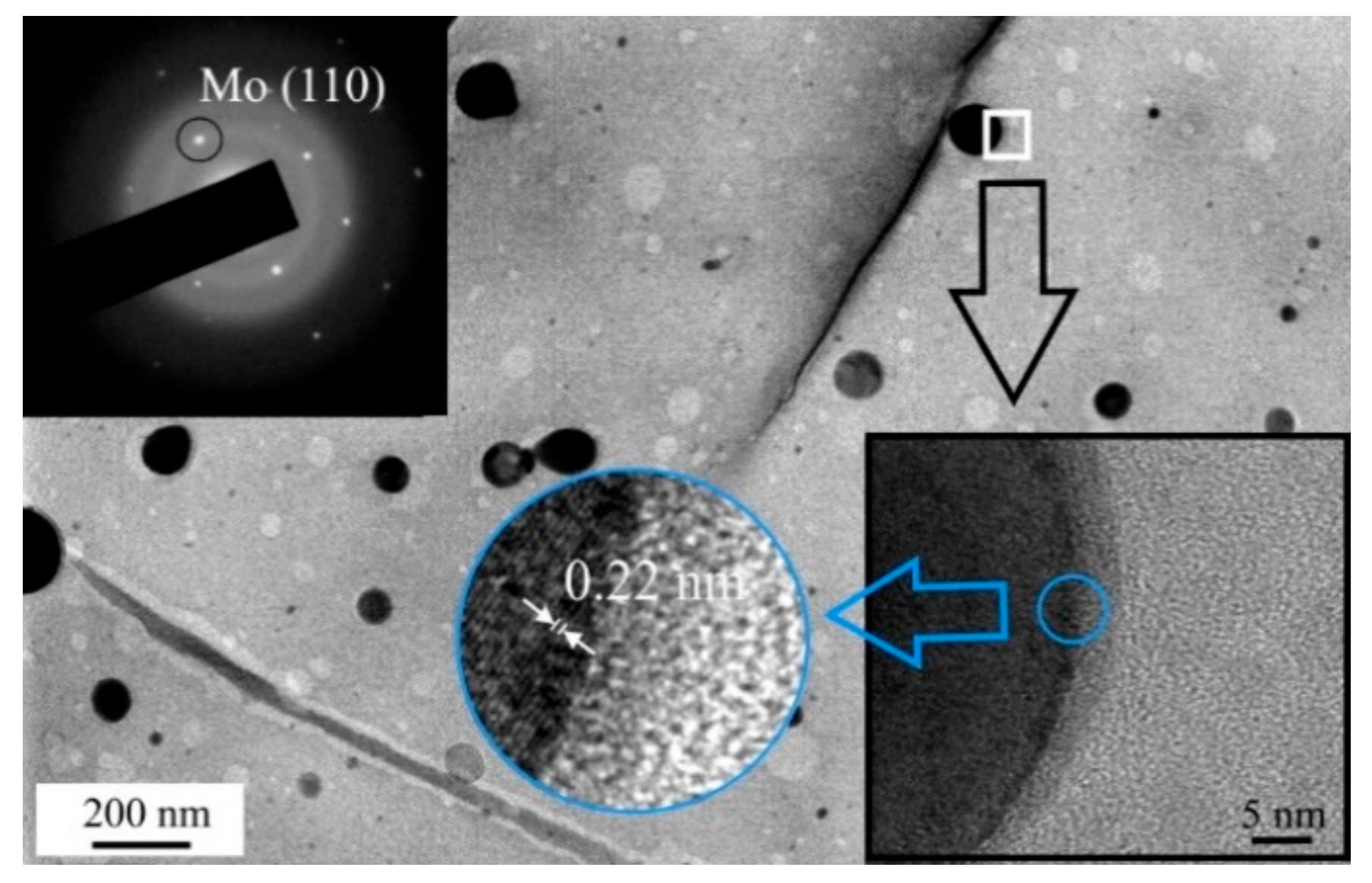
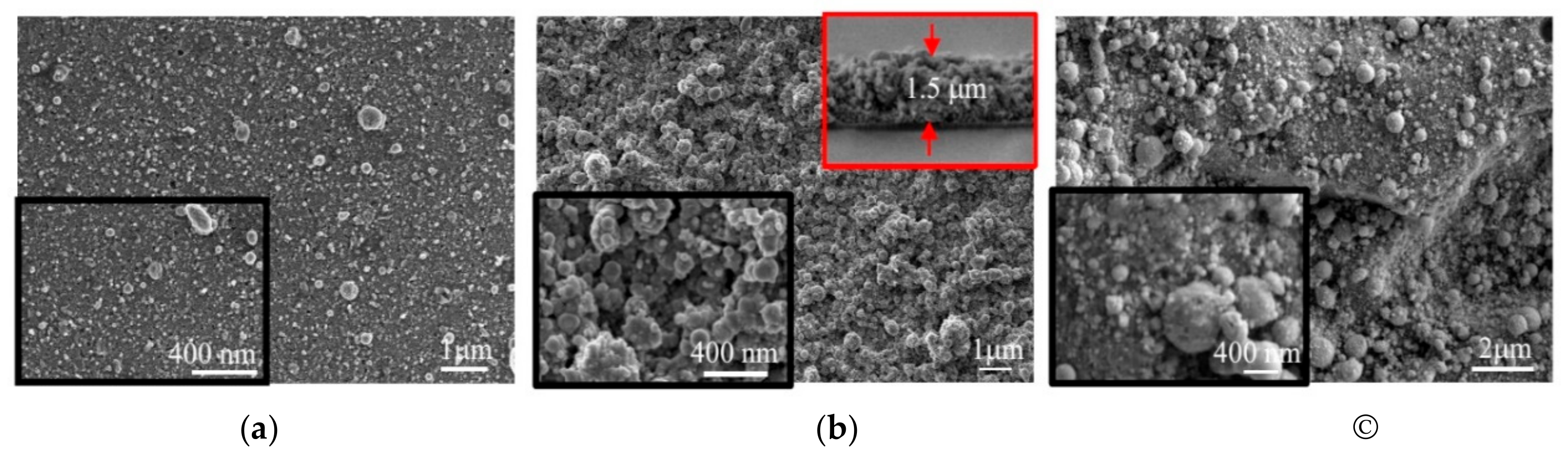
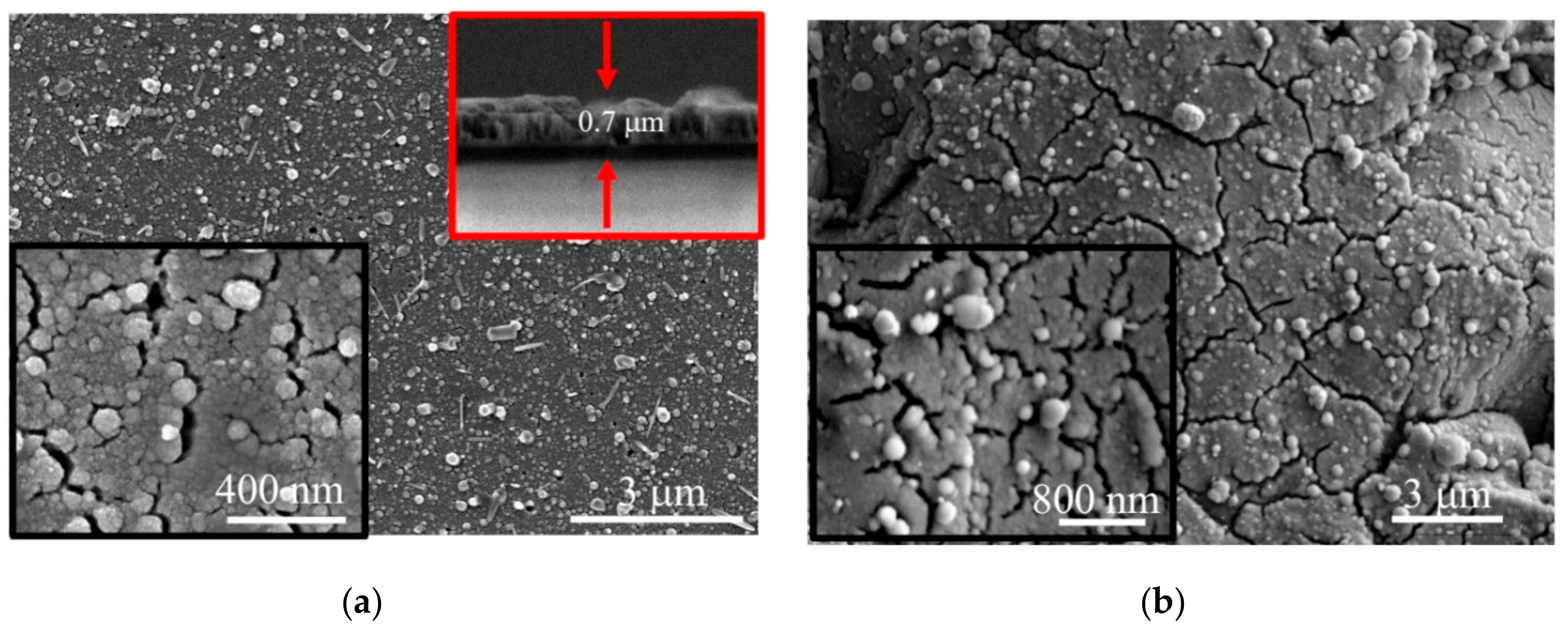
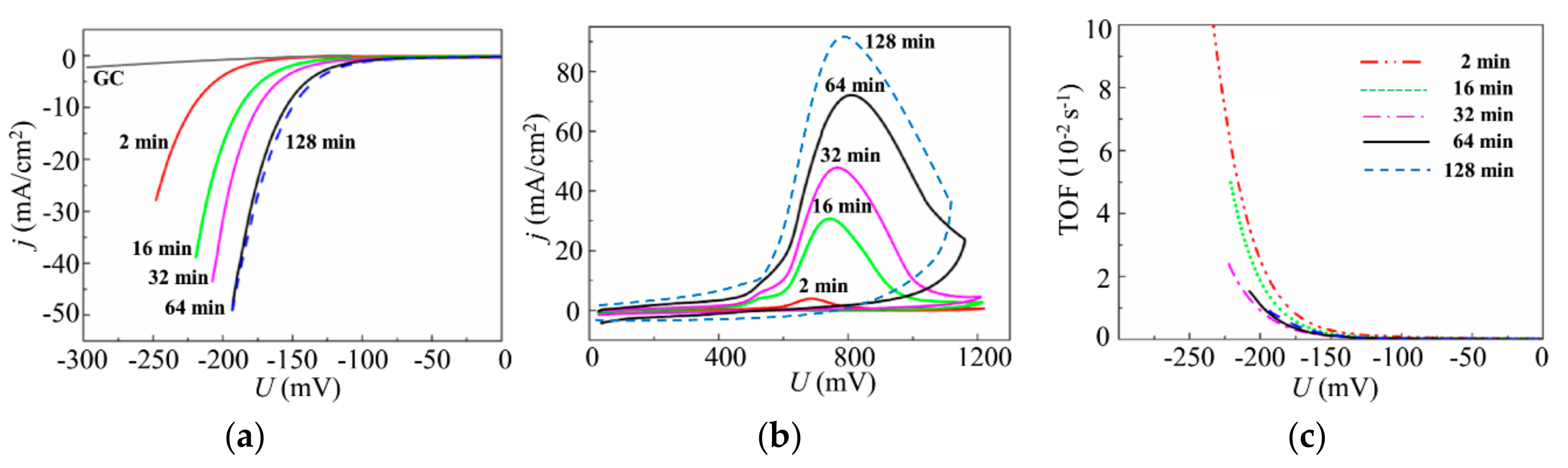
3.2. Deposition of the MoSx~2+δ/Mo Films by on-Axis PLD
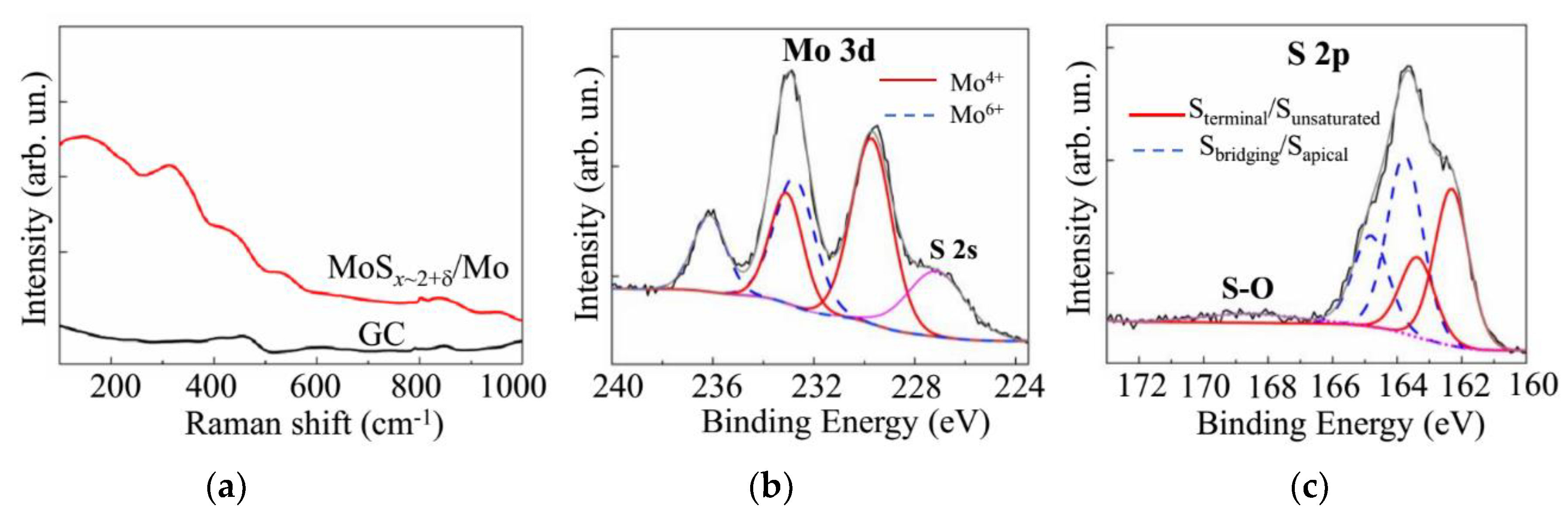
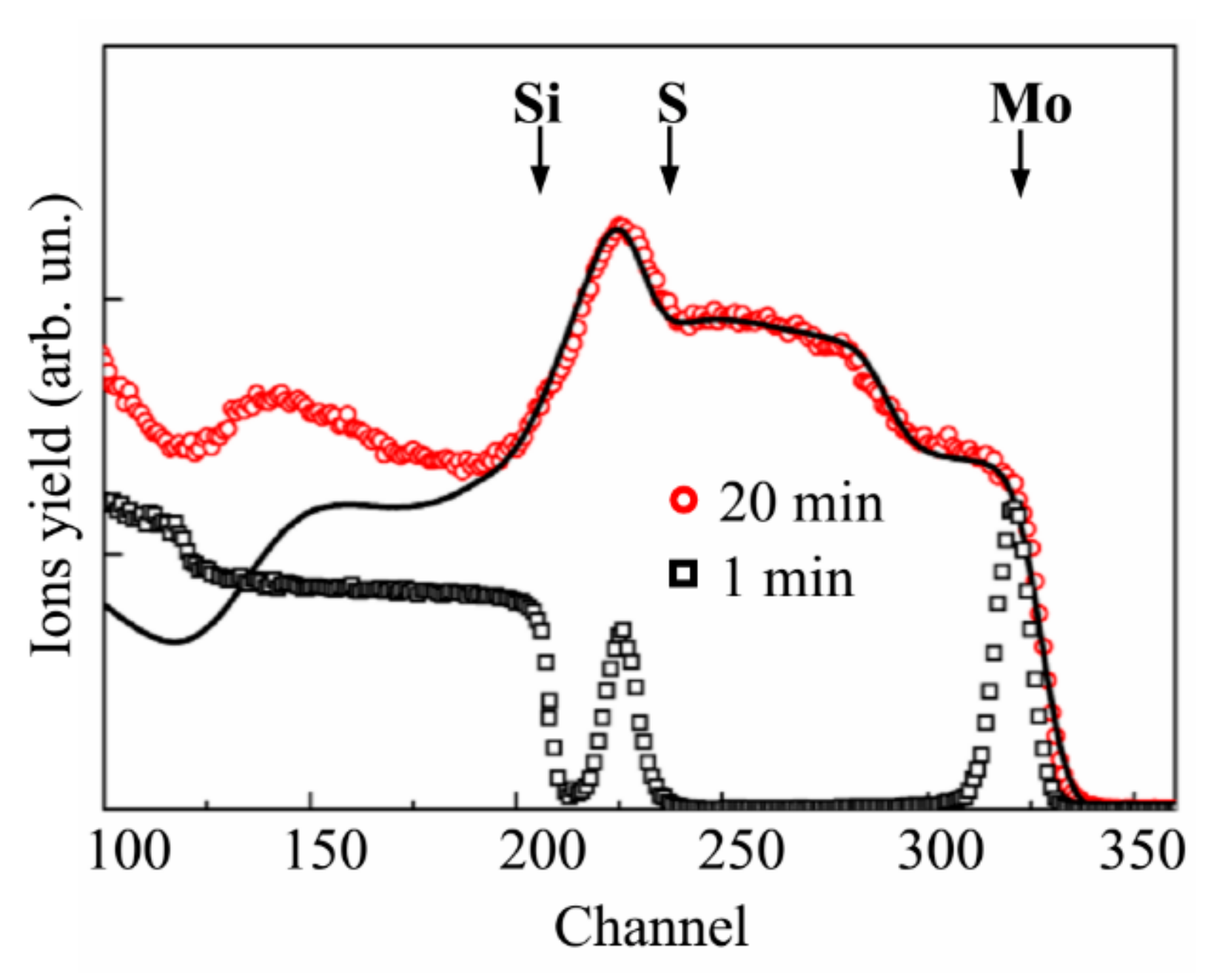
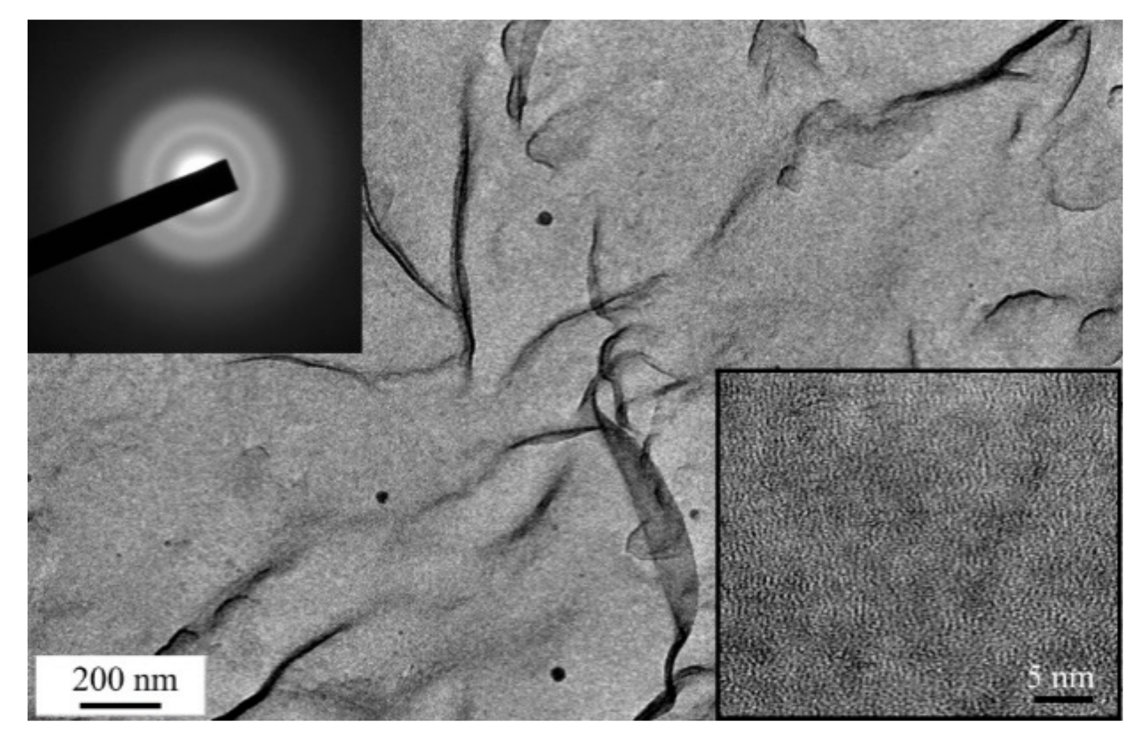
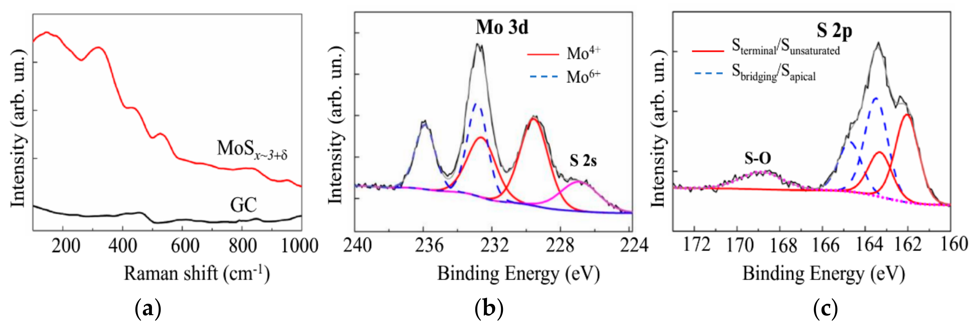
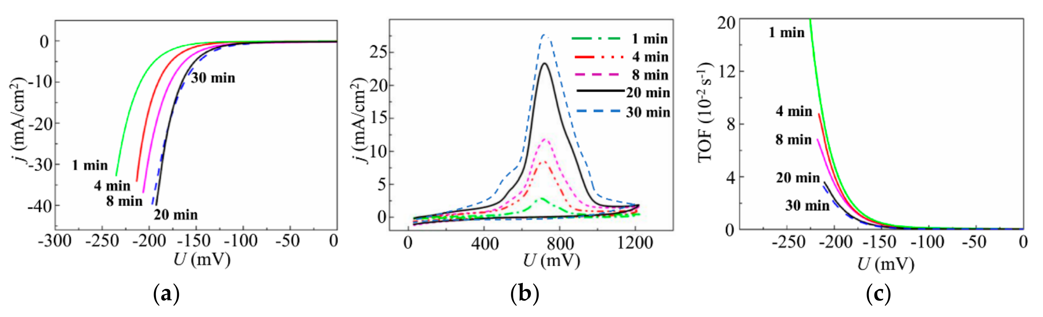
3.3. Deposition of the MoSx~3+δ Films by off-Axis PLD
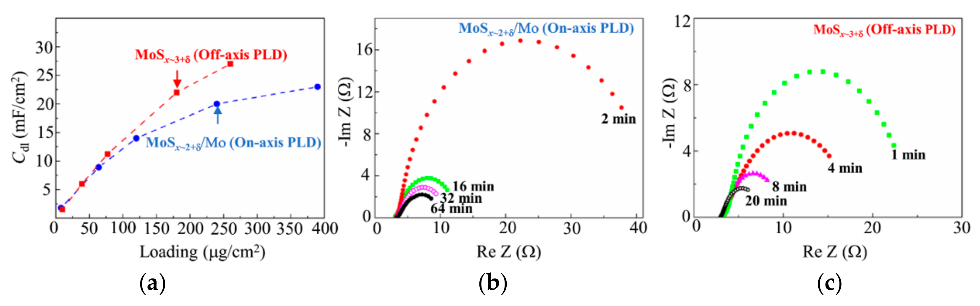
3.4. Electrocatalytic Performances of the MoSx~2+δ/Mo and MoSx~3+δ Films Prepared by on-Axis and off-Axis PLD
4. Discussion
5. Conclusions
Author Contributions
Funding
Conflicts of Interest
References
- Vesborg, P.C.K.; Seger, B.; Chorkendorff, I. Recent development in hydrogen evolution reaction catalysts and their practical implementation. J. Phys. Chem. Lett. 2015, 6, 951–957. [Google Scholar] [CrossRef]
- He, Z.; Que, W. Molybdenum disulfide nanomaterials: Structures, properties, synthesis and recent progress on hydrogen evolution reaction. Appl. Mater. Today 2016, 3, 23–56. [Google Scholar] [CrossRef]
- Niyitanga, T.; Jeong, H.K. Thermally reduced graphite oxide/carbon nanotubes supported molybdenum disulfide as catalysts for hydrogen evolution reaction. Int. J. Hydrog. Energy 2019, 44, 977–987. [Google Scholar] [CrossRef]
- Escalera-López, D.; Niu, Y.; Park, S.J.; Isaacs, M.; Wilson, K.; Palmer, R.E.; Rees, H.V. Hydrogen evolution enhancement of ultra-low loading, size-selected molybdenum sulfide nanoclusters by sulfur enrichment. Appl. Catal. B 2018, 235, 84–91. [Google Scholar] [CrossRef]
- Liu, Z.; Gao, Z.; Liu, Y.; Xia, M.; Wang, R.; Li, N. Heterogeneous nanostructure based on 1T phase MoS2 for enhanced electrocatalytic hydrogen evolution. ACS Appl. Mater. Interfaces 2017, 9, 25291–25297. [Google Scholar] [CrossRef] [PubMed]
- Kong, D.; Wang, H.; Cha, J.J.; Pasta, M.; Koski, K.J.; Yao, J.; Cui, Y. Synthesis of MoS2 and MoSe2 films with vertically aligned layers. Nano Lett. 2013, 13, 1341–1347. [Google Scholar] [CrossRef]
- Li, S.; Wang, S.; Salamone, M.M.; Robertson, A.W.; Nayak, S.; Kim, H.; Tsang, S.C.E.; Pasta, M.; Warner, J.H. Edge-enriched 2D MoS2 thin films grown by chemical vapor deposition for enhanced catalytic performance. ACS Catal. 2017, 7, 877–886. [Google Scholar] [CrossRef]
- Hinnemann, B.; Moses, P.G.; Bonde, J.; Jørgensen, K.P.; Nielsen, J.H.; Horch, S.; Chorkendorff, I.; Nørskov, J.K. Biomimetic hydrogen evolution: MoS2 nanoparticles as catalyst for hydrogen evolution. J. Am. Chem. Soc. 2005, 127, 5308–5309. [Google Scholar] [CrossRef]
- Jaramillo, T.F.; Jorgensen, K.P.; Bonde, J.; Nielsen, J.H.; Horch, S.; Chorkendorff, I. Identification of active edge sites for electrochemical H2 evolution from MoS2 nanocatalysts. Science 2007, 317, 100–102. [Google Scholar] [CrossRef]
- Li, H.; Tsai, C.; Koh, A.L.; Cai, L.; Contryman, A.W.; Fragapane, A.H.; Zhao, J.; Han, H.S.; Manoharan, H.C.; Pedersen, F.A.; et al. Activating and optimizing MoS2 basal planes for hydrogen evolution through the formation of strained sulphur vacancies. Nat. Mater. 2016, 15, 48–53. [Google Scholar] [CrossRef]
- Meng, C.; Lin, M.-C.; Du, X.-W.; Zhou, Y. Molybdenum disulfide modified by laser irradiation for catalyzing hydrogen evolution. ACS Sustain. Chem. Eng. 2019, 7, 6999–7003. [Google Scholar] [CrossRef]
- Morales-Guio, G.G.; Hu, X. Amorphous molybdenum sulfides as hydrogen evolution catalysts. Acc. Chem. Res. 2014, 47, 2671–2681. [Google Scholar] [CrossRef] [PubMed]
- Vrubel, H.; Hu, X. Growth and activation of an amorphous molybdenum sulfide hydrogen evolving catalyst. ACS Catal. 2013, 3, 2002–2011. [Google Scholar] [CrossRef]
- Merki, D.; Fierro, S.; Vrubel, H.; Hu, X. Amorphous molybdenum sulfide films as catalysts for electrochemical hydrogen production in water. Chem. Sci. 2011, 2, 1262–1267. [Google Scholar] [CrossRef]
- Fominski, V.Y.; Nevolin, V.N.; Romanov, R.I.; Fominski, D.V.; Dzhumaev, P.S. The influence of the local atomic packing of thin MoSx films on their electrocatalytic properties in hydrogen reduction. Tech. Phys. Lett. 2017, 43, 770–773. [Google Scholar] [CrossRef]
- Deng, Y.; Ting, L.R.L.; Neo, P.H.L.; Zhang, Y.-J.; Peterson, A.A.; Yeo, B.S. Operando Raman spectroscopy of amorphous molybdenum sulfide (MoSx) during the electrochemical hydrogen evolution reaction: Identification of sulfur atoms as catalytically active sites for H+ reduction. ACS Catal. 2016, 6, 7790–7798. [Google Scholar] [CrossRef]
- Xi, F.; Bogdanoff, P.; Harbauer, K.; Plate, P.; Höhn, C.; Rappich, J.; Wang, B.; Han, X.; van de Krol, R.; Fiechter, S. Structural transformation identification of sputtered amorphous MoSx as efficient hydrogen evolving catalyst during electrochemical activation. ACS Catal. 2019, 9, 2368–2380. [Google Scholar] [CrossRef]
- Escalera-López, D.; Lou, Z.; Rees, N.V. Benchmarking the activity, stability, and inherent electrochemistry of amorphous molybdenum sulfide for hydrogen production. Adv. Energy Mater. 2019, 9, 1802614. [Google Scholar] [CrossRef]
- Mabayoje, O.; Wygant, B.R.; Wang, M.; Liu, Y.; Mullins, C.B. Sulfur-rich MoS6 as an electrocatalyst for the hydrogen evolution reaction. ACS Appl. Energy Mater. 2018, 1, 4453–4458. [Google Scholar] [CrossRef]
- Afanasiev, P.; Jobic, H.; Lorentz, C.; Leverd, P.; Mastubayashi, N.; Piccolo, L.; Vrinat, M. Low-temperature hydrogen interaction with amorphous molybdenum sulfides MoSx. J. Phys. Chem. C 2009, 113, 4139–4146. [Google Scholar] [CrossRef]
- Song, X.; Chen, G.; Guan, L.; Zhang, H.; Tao, J. Interfacial engineering of MoS2/TiO2 hybrids for enhanced electrocatalytic hydrogen evolution reaction. Appl. Phys. Express 2016, 9, 095801. [Google Scholar] [CrossRef]
- Liu, B.; Jin, Z.; Bai, L.; Liang, J.; Zhang, Q.; Wang, N.; Liu, C.; Wei, C.; Zhao, Y.; Zhang, X. Molybdenum-supported amorphous MoS3 catalyst for efficient hydrogen evolution in solar-water splitting devices. J. Mater. Chem. A 2016, 4, 14204–14222. [Google Scholar] [CrossRef]
- Fominskii, V.Y.; Markeev, A.M.; Nevolin, V.N. Pulsed ion beams for modification of metal surface properties. Vacuum 1991, 42, 73–74. [Google Scholar] [CrossRef]
- Fominski, V.Y.; Nevolin, V.N.; Romanov, R.I.; Smurov, I. Ion-assisted deposition of MoSx films from laser-generated plume under pulsed electric field. J. Appl. Phys. 2001, 89, 1449–1457. [Google Scholar] [CrossRef]
- Muratore, C.; Voevodin, A.A. Control of molybdenum disulfide plane orientation during coating growth in pulsed magnetron sputtering discharges. Thin Solid Films 2009, 517, 5605–5610. [Google Scholar] [CrossRef]
- Wang, J.; Lauwerens, W.; Wieers, E.; Stals, L.M.; He, J.; Celis, J.P. Structure and tribological properties of MoSx coatings prepared by bipolar DC magnetron sputtering. Surf. Coat. Technol. 2001, 139, 143–152. [Google Scholar] [CrossRef]
- Fominski, V.Y.; Romanov, R.I.; Fominski, D.V.; Shelyakov, A.V. Regulated growth of quasi-amorphous MoSx thin-film hydrogen evolution catalysts by pulsed laser deposition of Mo in reactive H2S gas. Thin Solid Films 2017, 642, 58–68. [Google Scholar] [CrossRef]
- Wang, R.; Sun, P.; Wang, H.; Wang, X. Pulsed laser deposition of amorphous molybdenum disulfide films for efficient hydrogen evolution reaction. Electrochim. Acta 2017, 258, 876–882. [Google Scholar] [CrossRef]
- Fominski, V.Y.; Romanov, R.I.; Fominski, D.V.; Dzhumaev, P.S.; Troyan, I.A. Normal and grazing incidence pulsed laser deposition of nanostructured MoSx hydrogen evolution catalysts from a MoS2 target. Opt. Laser Technol. 2018, 102, 74–84. [Google Scholar] [CrossRef]
- Donley, M.S.; Murray, P.T.; Barber, S.A.; Haas, T.W. Deposition and properties of MoS2 thin films grown by pulsed laser evaporation. Surf. Coat. Technol. 1988, 36, 329–340. [Google Scholar] [CrossRef]
- Walck, S.D.; Zabinski, J.S.; Donley, M.S.; Bultman, J.E. Evolution of surface topography in pulsed-laser-deposited thin films of MoS2. Surf. Coat. Technol. 1993, 62, 412–416. [Google Scholar] [CrossRef]
- Grigoriev, S.N.; Fominski, V.Y.; Romanov, R.I.; Volosova, M.A.; Shelyakov, A.V. Pulsed laser deposition of nanocomposite MoSex/Mo thin-film catalyst for hydrogen evolution reaction. Thin Solid Films 2015, 592, 175–181. [Google Scholar] [CrossRef]
- Hu, J.J.; Zabinski, J.S.; Bultman, J.E.; Sanders, J.H.; Voevodin, A.A. Encapsulated nanoparticles produced by pulsed laser ablation of MoS2-Te composite target. Cryst. Growth Des. 2008, 8, 2603–2605. [Google Scholar] [CrossRef]
- Fominski, V.Y.; Grigoriev, S.N.; Gnedovets, A.G.; Romanov, R.I. On the mechanism of encapsulated particle formation during pulsed laser deposition of WSex thin-film coatings. Technol. Phys. Lett. 2013, 39, 312–315. [Google Scholar] [CrossRef]
- Fominski, V.Y.; Markeev, A.M.; Nevolin, V.N.; Prokopenko, V.B.; Vrublevski, A.R. Pulsed laser deposition of MoSx films in a buffer gas atmosphere. Thin Solid Films 1994, 248, 240–246. [Google Scholar] [CrossRef]
- Fominski, V.; Gnedovets, A.; Fominski, D.; Romanov, R.; Kartsev, P.; Rubinkovskaya, O.; Novikov, S. Pulsed laser deposition of nanostructured MoS3/np-Mo//WO3−y hybrid catalyst for enhanced (photo) electrochemical hydrogen evolution. Nanomaterials 2019, 9, 1395. [Google Scholar] [CrossRef]
- Deng, H.; Zhang, C.; Xie, Y.; Tumlin, T.; Giri, L.; Karna, S.P.; Lin, J. Laser induced MoS2/carbon hybrids for hydrogen evolution reaction catalysts. J. Mater. Chem. A 2016, 4, 6824–6830. [Google Scholar] [CrossRef]
- Ting, L.R.L.; Deng, Y.; Ma, L.; Zhang, Y.-J.; Peterson, A.A.; Yeo, B.S. Catalytic activities of sulfur atoms in amorphous molybdenum sulfide for the electrochemical hydrogen evolution reaction. ACS Catal. 2016, 6, 861–867. [Google Scholar] [CrossRef]
- Bailini, A.; Di Fonzo, F.; Fusi, M.; Casari, C.S.; Li Bassi, A.; Russo, V.; Baserga, A.; Bottani, C.E. Pulsed laser deposition of tungsten and tungsten oxide thin films with tailored structure at the nano- and mesoscale. Appl. Surf. Sci. 2007, 253, 8130–8135. [Google Scholar] [CrossRef]
- Fominski, V.Y.; Romanov, R.I.; Fominski, D.V.; Shelyakov, A.V. Preparation of MoSex>3/Mo-NPs catalytic films for enhanced hydrogen evolution by pulsed laser ablation of MoSe2 target. Nucl. Instrum. Methods Phys. Res. B 2018, 416, 30–40. [Google Scholar] [CrossRef]
- Wood, R.F.; Leboeuf, J.N.; Chen, K.R.; Geohegan, D.B.; Puretzky, A.A. Dynamics of plume propagation, splitting, and nanoparticle formation during pulsed-laser ablation. Appl. Surf. Sci. 1998, 127–129, 151–158. [Google Scholar] [CrossRef]
- McDevitt, N.T.; Bultman, J.E.; Zabinski, J.S. Study of amorphous MoS2 films grown by pulsed laser deposition. Appl. Spectrosc. 1998, 52, 1160–1164. [Google Scholar] [CrossRef]
- Luo, J.; Xu, P.; Zhang, D.; Wei, L.; Zhou, D.; Xu, W.; Li, J.; Yuan, D. Synthesis of 3D-MoO2 microsphere supported MoSe2 as an efficient electrocatalyst for hydrogen evolution reaction. Nanotechnology 2017, 28, 465404. [Google Scholar] [CrossRef] [PubMed]
- Kibsgaard, J.; Jaramillo, T.F.; Besenbacher, F. Building an appropriate active-site motif into a hydrogen-evolution catalyst with thiomolybdate [Mo3S13]2− clusters. Nat. Chem. 2014, 6, 248–253. [Google Scholar] [CrossRef] [PubMed]
- Tran, P.D.; Tran, T.V.; Orio, M.; Torelli, S.; Truong, Q.D.; Nayuki, K.; Sasaki, Y.; Chiam, S.Y.; Yi, R.; Honma, I.; et al. Coordination polymer structure and revisited hydrogen evolution catalytic mechanism for amorphous molybdenum sulfide. Nat. Mater. 2016, 15, 640–646. [Google Scholar] [CrossRef]
- Gnedovets, A.G.; Fominski, V.Y.; Nevolin, V.N.; Romanov, R.I.; Fominski, D.V.; Soloviev, A.A. Models of WOx films growth during pulsed laser deposition at elevated pressures of reactive gas. J. Phys. Conf. Ser. 2018, 941, 012064. [Google Scholar] [CrossRef]
- Chaudhari, N.K.; Jin, H.; Kim, B.; Lee, K. Nanostructured materials on 3D nickel foam as electrocatalysts for water splitting. Nanoscale 2017, 9, 12231–12247. [Google Scholar] [CrossRef]
- Kemppainen, E.; Halme, J.; Hansen, O.; Seger, B.; Lund, P.D. Two-phase model of hydrogen transport to optimize nanoparticle catalyst loading for hydrogen evolution reaction. Int. J. Hydrog. Energy 2016, 41, 7568–7581. [Google Scholar] [CrossRef]
- Kemppainen, E.; Halme, J.; Lund, P.D. An analytical model of hydrogen evolution and oxidation reactions on electrodes partially covered with a catalyst. Phys. Chem. Chem. Phys. 2016, 18, 13616–13628. [Google Scholar] [CrossRef]
- Huang, X.; Zhang, M.; Sun, R.; Long, G.; Liu, Y.; Zhao, W. Enhanced hydrogen evolution from CuOx-C/TiO2 with multiple electron transport pathways. PLoS ONE 2019, 14, e0215339. [Google Scholar] [CrossRef]
- Bharathi, N.D.; Sivasankaran, K. Influence of metal contact on the performance enhancement of monolayer MoS2 transistor. Superlattices Microstruct. 2018, 120, 479–486. [Google Scholar] [CrossRef]
- Fominski, V.Y.; Romanov, R.I.; Gnedovets, A.G.; Nevolin, V.N. Formation of the chemical composition of transition metal dichalcogenide thin films at pulsed laser deposition. Technical Phys. 2010, 55, 1509–1516. [Google Scholar] [CrossRef]


© 2020 by the authors. Licensee MDPI, Basel, Switzerland. This article is an open access article distributed under the terms and conditions of the Creative Commons Attribution (CC BY) license (http://creativecommons.org/licenses/by/4.0/).
Share and Cite
Fominski, V.; Demin, M.; Fominski, D.; Romanov, R.; Goikhman, A.; Maksimova, K. Comparative Study of the Structure, Composition, and Electrocatalytic Performance of Hydrogen Evolution in MoSx~2+δ/Mo and MoSx~3+δ Films Obtained by Pulsed Laser Deposition. Nanomaterials 2020, 10, 201. https://doi.org/10.3390/nano10020201
Fominski V, Demin M, Fominski D, Romanov R, Goikhman A, Maksimova K. Comparative Study of the Structure, Composition, and Electrocatalytic Performance of Hydrogen Evolution in MoSx~2+δ/Mo and MoSx~3+δ Films Obtained by Pulsed Laser Deposition. Nanomaterials. 2020; 10(2):201. https://doi.org/10.3390/nano10020201
Chicago/Turabian StyleFominski, V., M. Demin, D. Fominski, R. Romanov, A. Goikhman, and K. Maksimova. 2020. "Comparative Study of the Structure, Composition, and Electrocatalytic Performance of Hydrogen Evolution in MoSx~2+δ/Mo and MoSx~3+δ Films Obtained by Pulsed Laser Deposition" Nanomaterials 10, no. 2: 201. https://doi.org/10.3390/nano10020201
APA StyleFominski, V., Demin, M., Fominski, D., Romanov, R., Goikhman, A., & Maksimova, K. (2020). Comparative Study of the Structure, Composition, and Electrocatalytic Performance of Hydrogen Evolution in MoSx~2+δ/Mo and MoSx~3+δ Films Obtained by Pulsed Laser Deposition. Nanomaterials, 10(2), 201. https://doi.org/10.3390/nano10020201