Article

Ultrawide Bandgap and High Sensitivity of a Plasmonic Metal-Insulator-Metal Waveguide Filter with Cavity and Baffles

by
Yuan-Fong Chou Chau
1,*,
Chung-Ting Chou Chao
2,
Hung Ji Huang
3,
Muhammad Raziq Rahimi Kooh
1,
Narayana Thotagamuge Roshan Nilantha Kumara
1,
Chee Ming Lim
1 and
Hai-Pang Chiang
2,*
1
Centre for Advanced Material and Energy Sciences, Universiti Brunei Darussalam, Tungku Link, Gadong BE1410, Brunei
2
Department of Optoelectronics and Materials Technology, National Taiwan Ocean University, Keelung 20224, Taiwan
3
Taiwan Instrument Research Institute, National Applied Research Laboratories, Hsinchu 300, Taiwan
*
Authors to whom correspondence should be addressed.
Nanomaterials 2020, 10(10), 2030; https://doi.org/10.3390/nano10102030
Submission received: 5 September 2020 / Revised: 1 October 2020 / Accepted: 12 October 2020 / Published: 15 October 2020
(This article belongs to the Special Issue Nanobiophotonics, Photomedicine, and Imaging)

Abstract

:
A plasmonic metal-insulator-metal waveguide filter consisting of one rectangular cavity and three silver baffles is numerically investigated using the finite element method and theoretically described by the cavity resonance mode theory. The proposed structure shows a simple shape with a small number of structural parameters that can function as a plasmonic sensor with a filter property, high sensitivity and figure of merit, and wide bandgap. Simulation results demonstrate that a cavity with three silver baffles could significantly affect the resonance condition and remarkably enhance the sensor performance compared to its counterpart without baffles. The calculated sensitivity (S) and figure of merit (FOM) in the first mode can reach 3300.00 nm/RIU and 170.00 RIU−1. Besides, S and FOM values can simultaneously get above 2000.00 nm/RIU and 110.00 RIU−1 in the first and second modes by varying a broad range of the structural parameters, which are not attainable in the reported literature. The proposed structure can realize multiple modes operating in a wide wavelength range, which may have potential applications in the on-chip plasmonic sensor, filter, and other optical integrated circuits.

1. Introduction

Surface plasmon polaritons (SPPs) can use as electromagnetic (EM) wave transportation and confine EM wave at the dielectric–metal interface because of their capacities of handling light in the nanoscale [1,2,3,4,5,6,7,8,9,10,11,12,13,14,15]. A standard dielectric (or insulator) waveguide cannot form the EM wave beyond conventional optics’ diffraction limit [16]. Waveguides compose of an insulator placed between two metals term as metal-insulator-metal (MIM) waveguides possessing transmitting SPPs modes that are strongly restricted in a dielectric region with an adequate propagation length of SPPs [17,18,19]. A traditional plasmonic MIM waveguide consists of the straight waveguides and the resonance cavities [20,21]. Taking advantage of MIM waveguides, various plasmonic devices can be designed and manufactured [22,23,24,25,26,27,28]. Recently, cavity resonance formed in MIM waveguides to obtain wavelength filtering and refractive index sensing functions has been investigated by theoretical estimations and experimental verifications [29,30,31,32,33,34,35,36,37]. Several resonance modes can be excited in the straight waveguide coupled with the resonance cavity under SPPs conditions, which are highly sensitive to the refractive index’s variation and the cavity’s shape [38,39,40,41,42,43].
The resonance cavity in a MIM plasmonic waveguide system with different structural aspects plays a crucial role to form the SPPs modes in the resonance cavity. Various resonance cavities in plasmonic MIM waveguide using single or multiple cavities have theoretically analyzed and numerically investigated [44,45,46,47,48,49,50,51,52]. Many efforts have focused on enlarging the cavity size to achieve high sensitivity as the effective cavity length has a linear relationship to the increased resonance wavelength [20,37,53]. Although the higher sensitivity can be obtained, the drawback of enlarging device size and manufacturing complexity are presented.
Sensitivity and figure of merit are the two potential features for sensing performance. However, most efforts can only improve the above two factors in one spectrum channel, e.g., only one of the resonance modes has much higher sensitivity than the other modes [54,55,56,57,58,59]. Besides, most previous studies could not consider the influence of the cavity’s baffle effect in the resonance cavity and consider improving the two factors (i.e., S and FOM) in multiple channels (or multimode). The baffle’s influence could change the resonance condition that happened in the resonance cavity. The number of the geometrical parameters are suggested to be used as small as possible, since it is easier to optimize the parameters. The rectangular shape is the right choice because the straight edges compare to the figure with bent or complicated ones, e.g., ring shape, triangular, bowtie shape, and other combinations of different forms.
In this paper, a plasmonic metal-insulator-metal (MIM) waveguide refractive index sensor consisting of a rectangular cavity, including three silver (Ag) baffles, is designed and analyzed. We calculate the transmittance spectrum and magnetic Hz field distributions using a two-dimensional (2-D) finite element method (FEM) and examine the resonance modes in the rectangular cavity by the cavity resonance mode theory. The obtained results are approximately in line with the analytical ones. The influence of the structural parameters on the transmittance properties, refractive index sensitivity, and figure of merit was also explored. The proposed structure shows a simple shape with a small number of structural parameters that can function as a plasmonic sensor with a filter feature. One can demonstrate that a cavity with three baffles could significantly affect the resonance condition and remarkably enhance the sensor performance compared to its counter without the baffles. The proposed structure can realize multiple modes operating in a wide wavelength range, which may have potential applications in the on-chip plasmonic sensor, filter, and other nanophotonic devices in highly integrated optical circuits.

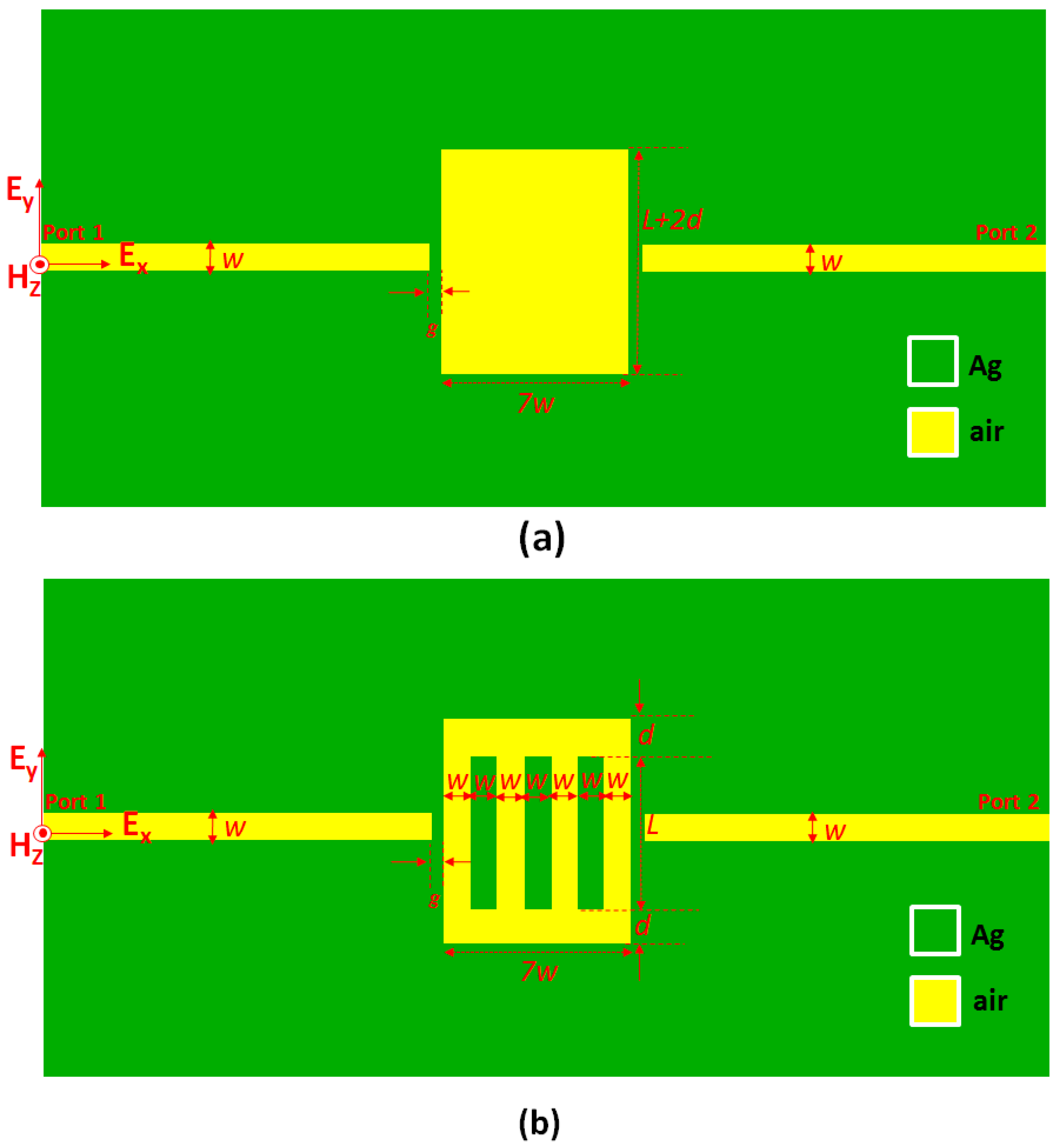
2. Structure Design and Simulation Method

Figure 1a,b depicts the schematic diagrams of the proposed plasmonic filters that consist of two straight waveguides and one central coupled rectangular cavity, excluding and including three silver (Ag) baffles with the same size. The Ag baffles (width w and length L) with adjacent gap distance w uniformly distribute in the rectangular cavity. The vertical coupling distance between the cavity edge and the Ag baffles is d. The straight waveguide width (w) is kept as 50 nm to ensure that the fundamental mode can transmit to the plasmonic MIM waveguide. Simulations were performed by a 2D FEM using the commercial software COMSOL Multiphysics (Version 5.2a, Stockholm, Sweden) [60] with perfectly matched layer absorbing boundary conditions to absorb the outgoing waves (to make sure that the light that is propagating out of the modeling domain does not get reflected). Note that a three-dimensional (3D) model is reduced to a 2D one since both models will obtain the similar results in simulations [49,61,62] and experiments [63,64], provided that the device height or thickness in the z-direction is much longer than in the x- and y- directions [52,65]. Therefore, we can ignore the effect of the device’s height on the obtained results by supposing that the device height is infinite [51]. Besides, the 2D approximation can speed up the simulation time and reduce the required computer resources, without sacrificing the calculation accuracy [66].
A TM-polarized incident EM wave with in-plane electric field component Ex along the x-direction is coupled to the plasmonic MIM waveguide system. Therefore, only the fundamental transverse magnetic (TM0) mode can be propagated in the waveguide, supporting SPPs waves [67]. In the FEM simulations, the transmittance (T) of the MIM waveguide is T = (S21)2, where S21 is the transmission coefficient from the input end (i.e., port 1) to the straight’s output end waveguides (i.e., port 2).
The two plasmonic nanometals are gold (Au) and silver (Ag). We chose Ag as a metal material because of the cost-consuming method for the proposed structure’s future fabrication. The oxidation of Ag can be controlled using a thin layer of SiO2 be deposited on the top to prohibit the direct exposure of Ag with air. The simulation works can also be available for the other metals (e.g., Au, Pt, etc.). The data of frequency-dependent complex relative permittivity εm of Ag is referred to Drude model as shown in Equation (1), and the dielectric constant of Ag is appropriate to describe the optical properties of Ag in the large wavelength range, which is considered in this work [32,68,69].
ε m ( ω ) = ε ω p 2 ω 2 + i ω γ   ,
where ω is the angular frequency of the incident EM wave. ε is the dielectric constant at the infinite frequency (ε = 3.7), ωp is the electron collision frequency (ωp = 1.38 × 10¹⁶ Hz = 9.10 eV), and γ is the bulk plasma frequency (γ = 2.37 × 10¹³ Hz = 18 meV). The resonance wavelength (λres) based on the cavity resonance mode theory can be described by [70,71,72]:
λ res = 2 e f f R e ( n eff ) m θ π   ( m = 1 , 2 , 3 ) ,
where λres is the resonance wavelength at transmittance peak, eff is the effective cavity length, and Re(neff) represents the real part of the effective refractive index. m is the mode number (positive number, i.e., m = 1, 2, 3,...), and θ is the phase. Based on the Equation (2), the λres can easily tune by varying the eff and neff of the rectangular cavity.
The sensitivity (S) can be calculated as S = Δλ/Δn nanometer per refractive index (nm/RIU), where Δλ is the shift of the resonance wavelength of transmittance, λres is the resonance wavelength at transmittance peak, and Δn is the refractive index difference. The figure of merit (FOM) is defined as S/FWHM, where FWHM is the full width at half-maximum of the transmittance spectrum. Besides, the quality factor can be defined as Q = λres/FWHM.
Thanks to the fast progress in nanophotonic, the fabrication of the proposed structure is achievable with current technologies [73,74,75,76,77,78,79,80,81,82,83,84,85,86,87,88], allowing the cost-effective fabrication over a large area. A similar structure of a MIM waveguide with a central-coupled rectangular cavity has previously been fabricated using physical vapor deposition and a focused ion beam for etching the rectangular cavity [79]. Another technology has also been proposed in [80], in which the straight waveguides and the rectangular cavity are formed by electron beam lithography. Moreover, wet chemical etching or vapor deposition techniques can provide a simple method for producing metal baffles [80,81]. However, the aim of this article is not to focus on fabrication methods. As an alternative, several potential papers that investigate in-depth coverage of this vital subject are suggested [76,77].

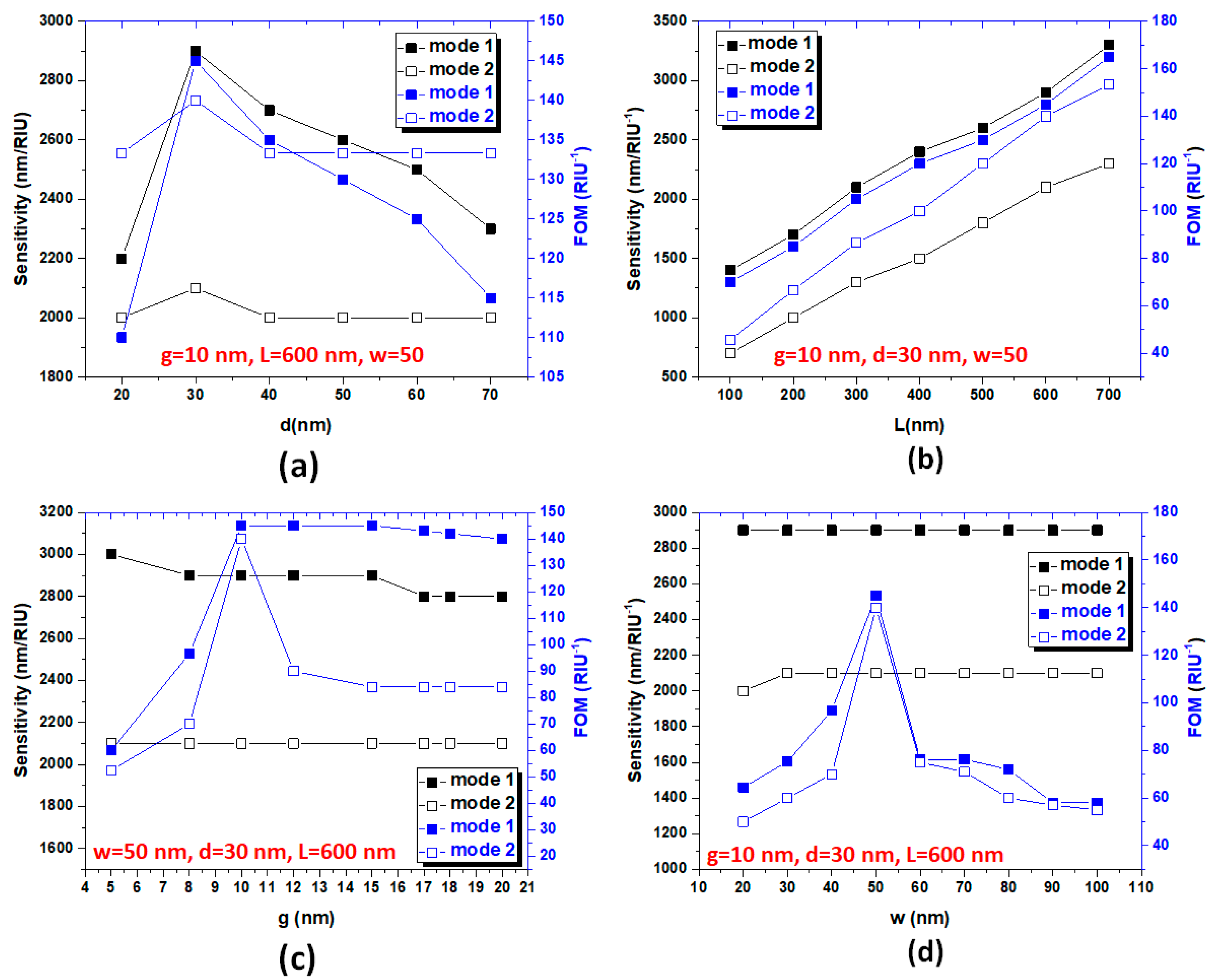
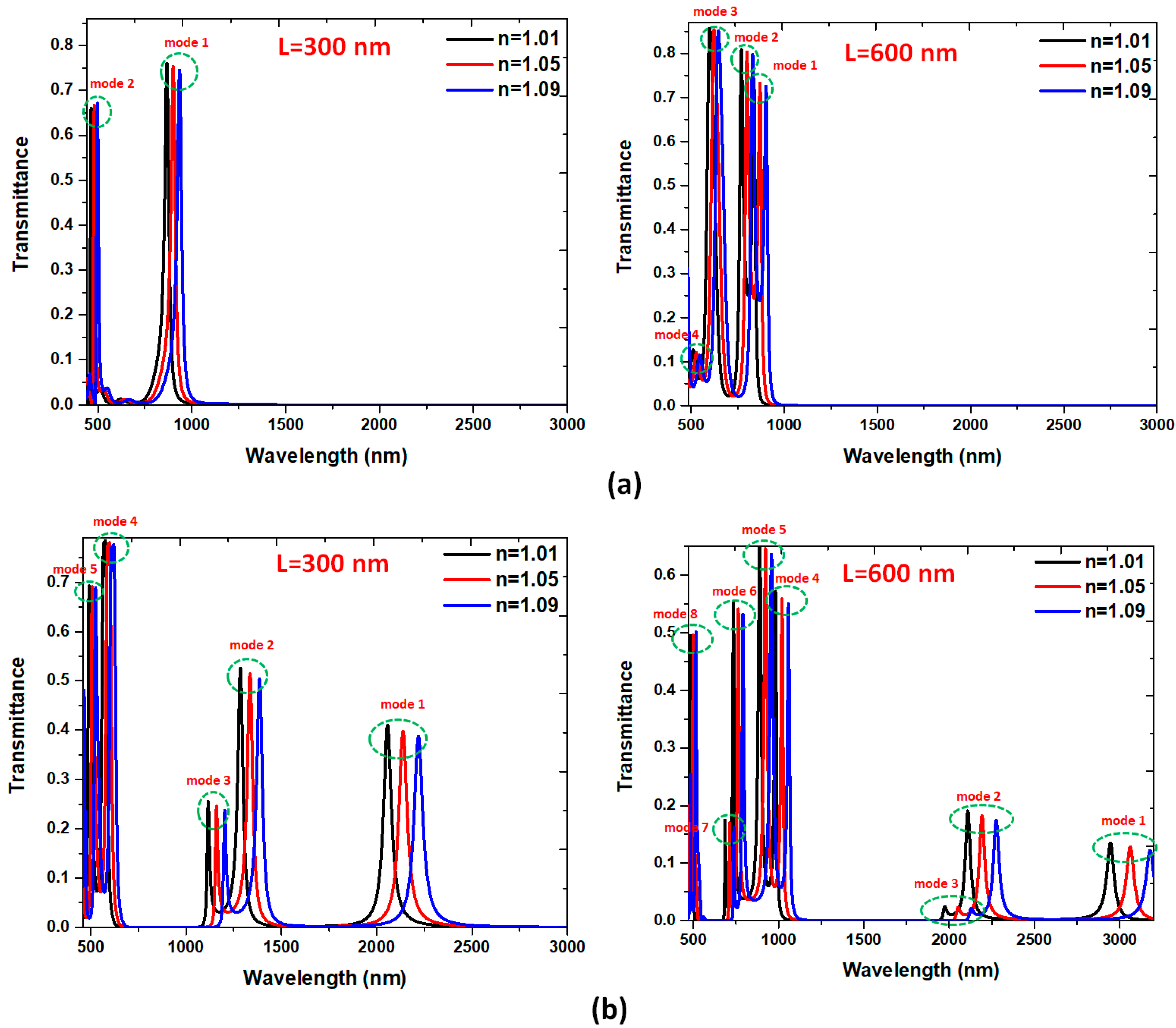
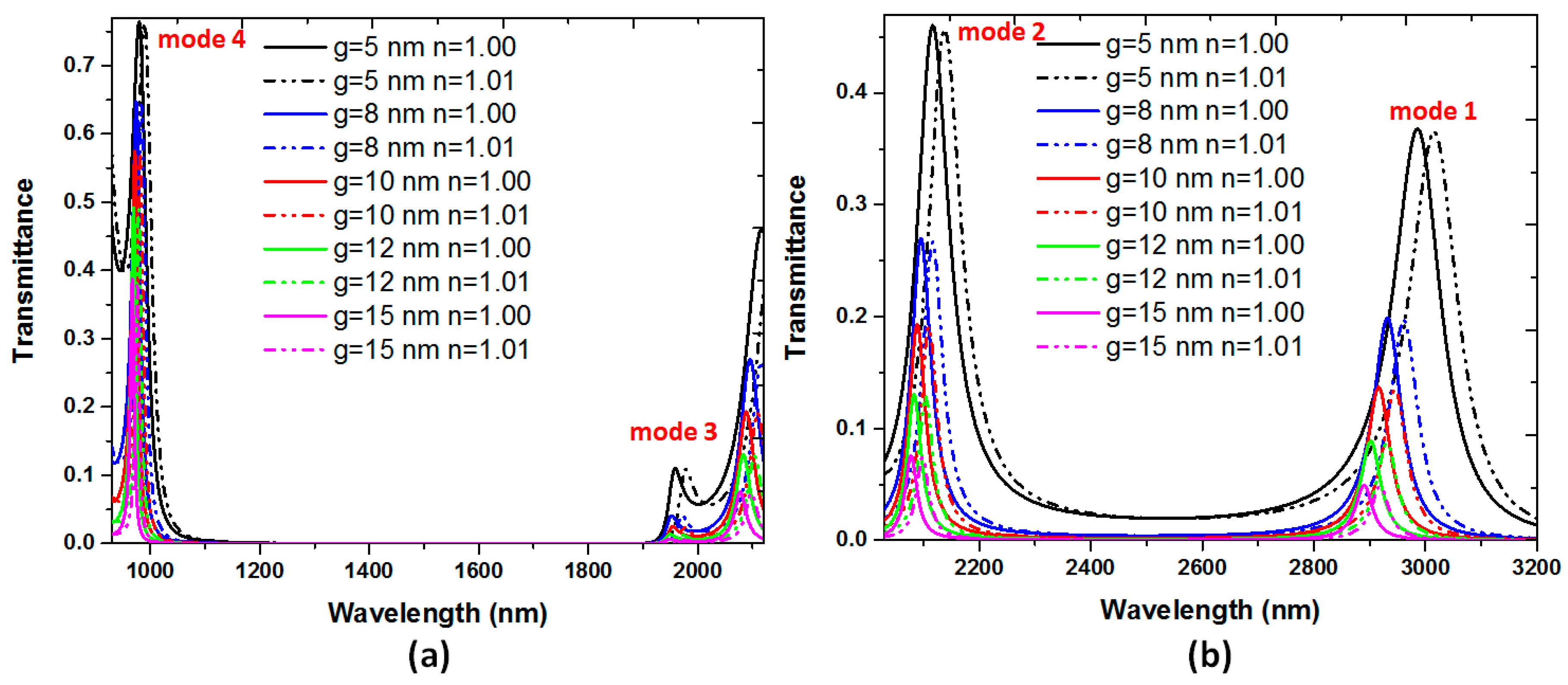
3. Results and Discussion

The proposed MIM waveguide plasmonic filter can serve as band-pass and band-stop filters, which permits and prohibits transmitting specific wavelengths of EM wave. However, narrow FWHM in pass-band and broad bandgap in stop-band is desirable in this plasmonic filter. We compared the proposed structures’ transmittance spectra without and with Ag baffles, as shown in Figure 2a,b, respectively. We use air (n = 1) as an insulator in the straight waveguides and rectangular cavity for simplicity. Two lengths of Ag baffles, i.e., L = 300 and L = 600 nm, are chosen for comparison. The other structural parameters, w, g, and d, are 50, 10, and 30 nm, respectively. An evident difference after the different lengths of Ag baffles are introduced in the MIM waveguide system, and the resonance condition difference can interpret this in the rectangular cavity. As seen in Figure 2a,b, only the Ag baffles cases reveal an apparent band-pass and band-stop profiles. More resonance modes could happen when the bigger cavity (i.e., longer L) is used. The Ag baffle case’s transmittance spectrum shows a prominent filtering characteristic with a narrow FWHM at the corresponding resonance modes in the rectangular cavity. In Figure 2a, two clear transmittance peaks were found at λres = 859 and 460 nm (marked by mode 1 and mode 2) concerning the case without Ag baffles for L = 300 nm and four ones were found at λres = 829, 762, 594, and 506 nm (marked by mode 1 to mode 4) concerning the case without Ag baffles for L = 600 nm, correspondingly. In Figure 2b, five clear transmittance peaks appeared at λres = 2036, 1273, 1106, 570, and 487 nm (marked by mode 1 to mode 5) and eight ones appeared at λres = 2916, 2088, 1955, 972, 880, 728, 680, and 478 nm (marked by mode 1 to mode 8) concerning the case with Ag baffles for L = 600 nm, correspondingly. These results show a noticeable increase in the λres when the Ag baffles are set in the rectangular cavity and the length of Ag baffles is increased. The case with Ag baffles (Figure 2b) shows a better performance compared to the case without Ag baffles (Figure 2a). The working wavelengths in the case without Ag baffles are in visible range, whereas in the case with Ag baffles, they can spread both in visible and near-infrared spectra. It is worth noting that the very sharp transmittance peaks can be seen in Figure 2a,b, indicating the proposed structure with the feature of high quality factor (Q factor). The calculated Q factors are 145.80, 139.20, 130.33, 97.2, 68.2, 176.00, 182.00, and 159.33 of mode 1 to mode 8, respectively, concerning the case with Ag baffles for L = 600 nm.
These transmittance peaks do not reach unity because of the metal’s internal loss in the proposal MIM waveguide system. Note that the SPP modes’ loss in larger wavelengths is more significant than those in smaller ones. This phenomenon is due to the SPP modes in larger wavelengths having more optical path and substantial power leaks from the MIM waveguides than the smaller ones, i.e., short wavelengths could decrease optical waveguide power consumption [82]. At λres, the SPPs mode in the rectangular cavity can be excited, and the EM wave can be transmitted. At the bandgap region (transmittance trough), the incident EM wave can be ultimately reflected.
In Figure 2b, there are two bandgap regions for L = 300 nm with bandgap width of Δλ = 420 and 500 nm, and three ones with bandgap width of Δλ =170, 870, and 540 nm for L = 600 nm, which does not appear in the case without baffles (i.e., no bandgap region between two transmittance peaks). Note that the bandgap width is significantly higher than those of the reported works [83,84]. In the proposed MIM waveguide, the transmittance raised maximum as the SPP modes fit the resonance condition in the rectangular cavity.
Based on Equation (2), λres is closely related to the neff and eff of the resonance cavity. The existence of Ag baffles may lead to the larger eff and neff for increasing λres (i.e., the redshift). It is worth noting that more transmittance peaks (or SPPs modes) and transmittance troughs (or bandgap regions) are preferred in the single plasmonic MIM waveguide system to fit the design of a miniaturized integrated optical circuit. The case with Ag baffles has more number of SPPs modes, which is superior to that of a small number of SPPs modes of the case without Ag buffers. The proposed structure with Ag baffles can be used as a multichannel on-chip plasmonic sensor with a filter function, and it also fits the requirement of the integrated optical circuits.
The SSPs modes found in Figure 2 are strongly dependent on the hybrid plasmonic effects of the gaps, cavity, and metal surfaces in the proposed MIM waveguide system [85,86,87,88,89]. The transmittance spectrum reveals a noticeable filtering feature at the corresponding resonance modes and bandgap regions. To interpreted the nature of Figure 2, we illustrated the magnetic field intensities (|H|) for the cases without and with the Ag baffles in the rectangular cavity at corresponding on-resonance modes (i.e., λres) and off-resonance modes concerning L = 300 nm (Figure 3a,b) and L = 600 nm (Figure 4a,b), respectively. The rectangular cavity can function as a Fabry–Pérot cavity, indicating that the EM waves can be transmitted through the rectangular cavity only when resonating with each other. As can be seen in band-pass cases in Figure 3 and Figure 4 that almost the SPPs wave is coupled to the rectangular cavity well at λres, and the |H| profiles show an entirely different patterns between the two cases. The mode patterns of |H| profiles are closely related to the size of incident wavelengths, i.e., shorter wavelength possesses more field lobes, whereas larger wavelength has fewer field lobes.
In the case with Ag baffles, the positive–negative charge pairs (or dipoles) distribute on the edge of the rectangular cavity surface and Ag baffles’ surface, resulting in the remarkable gap and cavity resonance compared to the case without Ag baffles. Besides, the case with Ag baffles contributes more dipoles, which will be beneficial for the coupling effects between nanometals and incident EM waves. Longer L could lead to more charge pairs on Ag baffles’ surface and the cavity edges. This characteristic can verify the |H| profiles in the case with Ag baffles (Figure 3b and Figure 4b), which show higher light enhancement and confinement between the metals in comparison to its counterpart without Ag baffles (Figure 3a and Figure 4a). In the case with Ag baffles, the EM waves can remarkably enlarge by the excitation of SPPs wave and the EM waves’ discontinuity across the straight waveguide interface, the rectangular cavity, and the Ag baffles. The resonance wavelength can be excited to the resonance mode, and the incident EM wave can be conveyed from the input end to the output end. As can be observed, the off-resonance mode in Figure 3 and Figure 4, the incident mode can be ultimately reflected at the left part of the straight waveguide and cavity (see Figure 3(a3,b6) and Figure 4(a5,b9)).
The proposed plasmonic filter can also apply as a refractive index sensor when the surrounding medium’s refractive index is changed. Figure 5a,b shows the proposed structure’s transmittance spectra without/with Ag baffles concerning L = 300 nm and L = 600 nm. To test the device’s sensitivity performance, we chose the refractive index values in the range of 1.01–1.09, and the other range of refractive index values has the same trend of transmittance spectrum based on our simulations [20]. The refractive index (n) is varied from 1.01, 1.05 to 1.09 at the interval of 0.04, respectively, while the other structural parameters w, g, and d are 50, 10, and 30 nm, respectively. As observed in Figure 5a,b, the transmission peaks show a redshift and a linear relationship with increasing n, which is in line with Equation (2). The redshift increase is due to the enhancing EM wave in a rectangular cavity, mostly interacting with the refractive index change. Since there is hybridization of the waveguide mode and the gap and cavity plasmon resonance modes in the rectangular cavity, a small refractive index change (Δn) results in a significant wavelength shift.
A suitable refractive index sensor simultaneously possesses the high sensitivity (S) and figure of merit (FOM) [90,91,92,93,94,95,96]. Figure 6 illustrates the resonance wavelength (λres) versus the refractive index (n) of the cases without and with Ag baffles concerning L = 600 nm in mode 1 to mode 4. The other structural parameters w, g, and d are 50, 10, and 30 nm. It found that a redshift of λres increases n, with a more massive shift in mode 1 and mode 2 than in other modes. Results show that the n can be estimated easily by certain λres according to Equation (2), demonstrating that the proposed structure’s features can function as a refractive index sensor. The S and FOM of the case without Ag baffles are 825.00 nm/RIU and 165.00 RIU−1 for mode 1, 750.00 nm/RIU and 150.00 RIU−1 for mode 2, 575.00 nm/RIU and 57.50 RIU−1 for mode 3, and 450.00 nm/RIU and 56.25 RIU−1 for mode 4, correspondingly. The higher average values of S and FOM can be achieved in the case with Ag baffles, i.e., 2900.00 nm/RIU and 145.00 RIU−1 for mode 1, 2100.00 nm/RIU and 140.00 RIU−1 for mode 2, 2000.00 nm/RIU and 200.00 RIU−1 for mode 3, 1000.00 nm/RIU and 200.00 RIU−1 for mode 4, 900.00 nm/RIU and 180.00 RIU−1 for mode 5, 700.00 nm/RIU and 175.00 RIU−1 for mode 6, 600.00 nm/RIU and 200.00 RIU−1 for mode 7, and 600.00 nm/RIU and 300.00 RIU−1 for mode 8, correspondingly. Compared to the case without Ag baffles, the case’s performance with Ag baffles in the rectangular cavity generates an enhancement of filter’s sensitivity by 251.50% for mode 1, 180% for mode 2, 247.83% for mode 3, and 122.22% for mode 4. These values are remarkable and highly satisfy the request of plasmonic refractive index sensor. It is worth noting that it can simultaneously achieve higher sensitivity and figure of merit, which are larger than 2000.00 nm/RIU and 140.00 RIU−1 in mode 1 to mode 3 in our design. The proposed structure is appropriate for working as a gas sensor or in a liquid environment. The reason is that the gas sensors usually require higher sensitivity since the refractive index changes are small, while lower sensitivity might be tolerable in water.
Subsequently, we discuss the influence of structural parameters on sensitivities and figure of merit of the proposed structure. For simplifying the optimization of the structural parameters, the number of structural parameters is used as small as possible. Fortunately, only four structural parameters (i.e., w, g, d, and L) are considered in our design. In the previous simulations, we fixed w = 50 nm for the fundamental mode to excite the straight waveguide and g = 10 nm for efficient coupling between the straight waveguide and the cavity [20,32]. Next, the four structural parameters, d, L, w, and g, will be inspected in detail. The air region’s resonance condition in the rectangular cavity can be changed by varying the value of d and L since the air region between Ag baffles, and the cavity edges has been changed, resulting in a variation of neff and eff in the resonance cavity. Similarity, the straight waveguide width (w) and horizontal coupling distance (g) could affect the propagating mode in the straight waveguide and resonance condition in the rectangular cavity. Figure 7a,b shows the sensitivities and figure of merit of the proposed plasmonic sensor with Ag baffles in mode 1 and mode 2 for varying coupling distance (d) from 10 to 70 nm in the step of 10 nm and for varying Ag baffle’s length (L) from 300 to 700 nm in the step of 100 nm, respectively. The other structural parameters are denoted in the inset of the figures. In Figure 7a, the variation of d in the range of 20–70 nm demonstrates that the proposed structure’s sensitivity and FOM simultaneously achieve above 2000.00 nm/RIU and 110.00 RIU−1 in modes 1 and 2, revealing the robustness of manufacturing. These results with high sensitivity and figure of merit in mode 1 and mode 2 cannot be simultaneously obtained in the reported literature (e.g., [97,98,99,100,101,102]). The optimal value is d = 30 nm, which can support the plasmon resonance mode to enhance the proposed structure’s sensitivity and FOM. As can be seen in Figure 7b, the Ag baffle’s length (L) can significantly influence the sensitivity and figure of merit with L’s increase when L is in the range of 100–700 nm. The highest sensitivity can reach S = 3300.00 nm/RIU along with a high FOM of 170.00 RIU−1 and ultrawide bandgap (results not shown here). According to the simulations and analysis above, the proposed plasmonic filter’s function can easily tune by changing the d and L set in the rectangular cavity. Therefore, one can vary d and L in the rectangular cavity to design the band-pass and band-stop plasmonic filter with the desired working wavelength.
Figure 7c,d shows the sensitivities and figure of merit of the proposed plasmonic sensor with Ag baffles in mode 1 and mode 2 for varying coupling distance (g) in the range of 5–20 nm and for varying the straight waveguide width (w) from 20 to 100 nm in the step of 10 nm, respectively. In Figure 8a, b the structural parameters g and w can also affect the proposed structure’s SPPs mode as well as resonance condition. As observed, the sensitivity shows the same trend and simultaneously reaches above 2000.00 nm/RIU in mode 1 and mode 2 in a wide range of g and w, while the FOM reveals the different values due to the different FWHM. Based on our simulations, the higher transmission can generate a larger extinction ratio and a smaller FWHM, contributing to a larger FOM. In Figure 7c,d, the optimal values are g = 10 nm and w = 50 nm, respectively. These features found in Figure 7a–d can explain by the increase in eff and neff in the rectangular cavity, as indicated in Equation (2). It is worth noting that a problem on how well can these FOM and S be reproduced by an experimental structure and given a fabrication tolerance. The suggested structural parameters of the proposed plasmonic sensor are in the range of 20 nm < d <70 nm, 300 nm < L < 700 nm, 5 nm < g < 15 nm, and 40 nm < w <70 nm, respectively. The high sensitivity and figure of merit can also be achieved in a broad-spectrum range for promising applications in nanophotonics. With the recent advances in plasmonic sensors, there is an anticipation of enhancing sensitivity and reducing the detection limit to overcome the limitations in ultrasensitive sensing of biological and chemical analytes, especially at single molecule levels [103,104,105].
Finally, we investigate in more detail the influence of coupling distance g on the transmittance, since the structural parameter g of 10 nm would be rather difficult to control experimentally [78]. Figure 8 depicts the transmittance spectrum of the proposed plasmonic filter of mode 3 and mode 4 (Figure 8a) and mode 1 and mode 2 (Figure 8b) versus different coupling distances (g) and different refractive indices (n). The g values are varied from 5, 8, 10, 12 to 15 nm, and n values are changed from 1.00 to 1.01. We focus on the transmittance peaks and bandgap width in modes 1 to mode 3, while the other structural parameters are kept as w = 50, d = 30 nm, L = 600 nm, respectively. As observed, the transmittance peaks decrease with the increase of g because of the less coupling and more propagation loss between the straight waveguides and the rectangular cavity. Besides, the resonance wavelengths reveal slight blueshift to shorter wavelengths for a larger g, which well agrees with the reported literature [106]. The transmittance shift is about 20, 29, 29, 29, and 29 nm in mode 1 and 21, 21, 21, 21, and 21 nm in mode 2, when g varies from 5, 8, 10, 12 to 15 nm, correspondingly. In these cases, the sensitivity in mode 1 and mode 2 can simultaneously exceed 2000.00 nm/RIU when g in the range of 5–15 nm, indicating that the proposed structure possesses a high fabrication tolerance. It is evident that the parameter g is not only affecting the transmittance spectrum but also influences the transmission bands’ line shape. As seen in Figure 8b, the bandgap width between mode 1 and mode 2 is increased as the g value increases, while the bandgap width between mode 3 and mode 4 remains unchanged (see Figure 8a). It is also important to note that, there is no bandgap (or transmittance through) between mode 1 and mode 2 when g = 5 nm, since a narrow coupling distance leads to more coupling effect between the straight waveguide and the rectangular cavity.

4. Conclusions

In conclusion, we have proposed a simple designed plasmonic MIM filter with a high sensitivity and a high figure of merit as well as a wide bandgap. The proposed structure consists of two straight waveguides, three Ag baffles, and one rectangular cavity. The sensitivity and figure of merit of the structure can be improved by varying two structural parameters, i.e., the length of Ag baffles (L) and the coupling distance between the baffles and cavity (d). Results show the obvious on-resonance and off-resonance modes and narrow FWHM in the proposed structures due to the hybrid plasmonic coupling effect of the metal’s surfaces, gaps, and cavities. The proposed design has a simple shape with a small number of structural parameters, making it easy for integration and optimization. The highest sensitivity of 3300.00 nm/RIU and figure of merit of 170.00 RIU−1 can be achieved. The variation of d in the range of 20–70 nm demonstrates that the proposed structure’s sensitivity and figure of merit can simultaneously achieve above 2000.00 nm/RIU and 110.00 RIU−1 in the first and second modes, which cannot obtain from the reported literature. FEM simulations investigated the simulation results, and it believed that the proposed structure can support full application in the on-chip optical sensing and filtering areas. Besides, these simulation results obtained from FEM are in good agreement with the cavity resonance mode theory.

Author Contributions

Y.-F.C.C. and C.-T.C.C. conceived and carried out the simulations; Y.-F.C.C. and H.-P.C. designed the study; H.J.H., M.R.R.K., N.T.R.N.K., and C.M.L. analyzed the data and wrote the manuscript. All authors have read and agreed to the published version of the manuscript.

Funding

This work was supported by the University Research Grant of Universiti Brunei Darussalam (Grant No. UBD/RSCH/1.9/FICBF(b)/2019/006) and the Ministry of Science and Technology of Taiwan (MOST 106-2112-M-019-005-MY3 and MOST 109-2112-M-019-005-001).

Conflicts of Interest

The authors have no conflict of interest to declare.

References

  1. Chen, W.T.; Wu, P.C.; Chen, C.J.; Chung, H.Y.; Chau, Y.; Kuan, C.H.; Tsai, D.P. Electromagnetic energy vortex associated with sub-wavelength plasmonic Taiji marks. Opt. Express 2010, 18, 19665–19671. [Google Scholar] [CrossRef] [PubMed]
  2. Guo, Z.; Wen, K.; Hu, Q.; Lai, W.; Lin, J.; Fang, Y. Plasmonic multichannel refractive index sensor based on subwavelength tangent-ring metal–insulator–metal waveguide. Sensors 2018, 18, 1348. [Google Scholar] [CrossRef] [PubMed] [Green Version]
  3. Chau, Y.; Tsai, D.P. Three-dimensional analysis of silver nano-particles doping effects on super resolution near-field structure. Opt. Commun. 2007, 269, 389–394. [Google Scholar] [CrossRef]
  4. Hsieh, L.-Z.; Chau, Y.; Lim, C.; Lin, M.-H.; Huang, H.J.; Lin, C.-T.; Syafi’Ie, I.M.N. Metal nano-particles sizing by thermal annealing for the enhancement of surface plasmon effects in thin-film solar cells application. Opt. Commun. 2016, 370, 85–90. [Google Scholar] [CrossRef]
  5. Sung, M.J.; Ma, Y.F.; Chau, Y.; Huang, D.W. Plasmon field enhancement in silver core-protruded silicon shell nanocylinder illuminated with light at 633 nm. Appl. Opt. 2010, 49, 6295–6301. [Google Scholar] [CrossRef] [PubMed]
  6. Chou, Y.; Yeh, H.-H.; Tsai, D.P. Surface plasmon effects excitation from three-pair arrays of silver-shell nanocylinders. Phys. Plasmas 2009, 16, 22303. [Google Scholar] [CrossRef]
  7. Hayashi, S.; Nesterenko, D.V.; Sekkat, Z. Waveguide-coupled surface plasmon resonance sensor structures: Fano lineshape engineering for ultrahigh-resolution sensing. J. Phys. D Appl. Phys. 2015, 48, 325303. [Google Scholar] [CrossRef]
  8. Najafabadi, M.M.; Vahidi, S.; Ghafoorifard, H.; Valizadeh, M. Single-channel high-transmission optical band-pass filter based on plasmonic nanocavities. J. Opt. Soc. Am. B 2020, 37, 2329–2337. [Google Scholar] [CrossRef]
  9. Ho, Y.Z.; Chen, W.T.; Huang, Y.-W.; Wu, P.C.; Tseng, M.L.; Wang, Y.T.; Chau, Y.-F.C.; Tsai, D.P. Tunable plasmonic resonance arising from broken-symmetric silver nanobeads with dielectric cores. J. Opt. 2012, 14, 114010. [Google Scholar] [CrossRef]
  10. Hu, C.; Yang, W.; Tsai, Y.T.; Chau, Y.F. Gap enhancement and transmittance spectra of a periodic bowtie nanoantenna array buried in a silica substrate. Opt. Commun. 2014, 324, 227–233. [Google Scholar] [CrossRef]
  11. Lin, C.-T.; Chang, M.-N.; Huang, H.J.; Chen, C.-H.; Sun, R.-J.; Liao, B.-H.; Chau, Y.; Hsiao, C.-N.; Shiao, M.-H.; Tseng, F.-G. Rapid fabrication of three-dimensional gold dendritic nanoforests for visible light-enhanced methanol oxidation. Electrochim. Acta 2016, 192, 15–21. [Google Scholar] [CrossRef]
  12. Shen, L.; Yang, T.J.; Chau, Y. Effect of internal period on the optical dispersion of indefinite-medium materials. Phys Rev. B 2008, 77, 205124. [Google Scholar] [CrossRef] [Green Version]
  13. Jankovic, N.; Cselyuszka, N. Multiple Fano-Like MIM Plasmonic Structure Based on Triangular Resonator for Refractive Index Sensing. Sensors 2018, 18, 287. [Google Scholar] [CrossRef] [PubMed] [Green Version]
  14. Li, M.; Cushing, S.K.; Wu, N. Plasmon-enhanced optical sensors: A review. Analyst. 2015, 140, 386–406. [Google Scholar] [CrossRef] [PubMed] [Green Version]
  15. Hu, C.-C.; Tsai, Y.-T.; Yang, W.; Chau, Y. Effective Coupling of Incident Light Through an Air Region into an S-Shape Plasmonic Ag Nanowire Waveguide with Relatively Long Propagation Length. Plasmonics 2014, 9, 573–579. [Google Scholar] [CrossRef]
  16. Chau, Y.; Yang, T.J.; Lee, W.D. Coupling technique for efficient interfacing between silica waveguides and planar photonic crystal circuits. Appl. Opt. 2004, 43, 6656–6663. [Google Scholar] [CrossRef] [PubMed] [Green Version]
  17. Fang, Y.; Sun, M. Nanoplasmonic waveguides: Towards applications in integrated nanophotonic circuits. Light. Sci. Appl. 2015, 4, e294. [Google Scholar] [CrossRef] [Green Version]
  18. Chen, J.J.; Sun, C.W.; Hu, X.Y. Nanoscale all-optical devices based on surface plasmon polaritons. Chinese Sci. Bull. 2014, 59, 2661–2665. [Google Scholar] [CrossRef]
  19. Kim, N.C.; Ko, M.C.; Wang, Q.Q. Single plasmon switching with n quantum dots system coupled to one-dimensional waveguide. Plasmonics 2015, 10, 611–615. [Google Scholar] [CrossRef] [Green Version]
  20. Chou Chao, C.-T.; Chou Chau, Y.; Huang, H.J.; Kumara, N.T.R.N.; Kooh, M.R.R.; Lim, C.M.; Chiang, H.-P. Highly Sensitive and Tunable Plasmonic Sensor Based on a Nanoring Resonator with Silver Nanorods. Nanomaterials 2020, 10, 1399. [Google Scholar] [CrossRef]
  21. Chou Chau, Y.F. Mid-infrared sensing properties of a plasmonic metal–insulator–metal waveguide with a single stub including defects. J. Phys. D Appl. Phys. 2020, 53, 115401. [Google Scholar] [CrossRef]
  22. Zhao, H.; Huang, X.; Huang, J. Surface plasmon polaritons based optical directional coupler. Sci. China Ser. G Phys. Mech. Astron. 2008, 51, 1877–1882. [Google Scholar] [CrossRef]
  23. Matsubara, K.; Kawata, S.; Minami, S. Optical chemical sensor based on surface plasmon measurement. Appl. Opt. 1988, 27, 1160–1163. [Google Scholar] [CrossRef] [PubMed]
  24. Zhang, Z.; Luo, L.; Xue, C.; Zhang, W.; Yan, S. Fano Resonance Based on Metal-Insulator-Metal Waveguide-Coupled Double Rectangular Cavities for Plasmonic Nanosensors. Sensors. 2016, 16, 642. [Google Scholar] [CrossRef] [PubMed] [Green Version]
  25. Hu, F.; Yi, H.; Zhou, Z. Wavelength demultiplexing structure based on arrayed plasmonic slot cavities. Opt. Lett. 2011, 36, 1500–1502. [Google Scholar] [CrossRef]
  26. Drezet, A.; Hohenau, A.; Stepanov, A.L.; Ditlbacher, H.; Steinberger, B.; Aussenegg, F.R.; Leitner, A.; Krenn, J.R. Surface plasmon polariton Mach–Zehnder interferometer and oscillation fringes. Plasmonics 2006, 1, 141–145. [Google Scholar] [CrossRef]
  27. Zhang, Z.; Wang, J.; Zhao, Y.; Lu, D.; Xiong, Z. Numerical investigation of a branch-shaped filter based on metal-insulator-metal waveguide. Plasmonics 2011, 6, 773–778. [Google Scholar] [CrossRef]
  28. Kazanskiy, N.L.; Khonina, S.N.; Butt, M.A. Plasmonic sensors based on Metal-insulator-metal waveguides for refractive index sensing applications: A brief review. Physica E 2020, 117, 113798. [Google Scholar] [CrossRef]
  29. Tong, L.M.; Wei, H.; Zhang, S.P.; Xu, H.X. Recent advances in plasmonic sensors. Sensors 2014, 14, 7959–7973. [Google Scholar] [CrossRef] [Green Version]
  30. Qi, J.; Chen, Z.; Chen, J.; Li, Y.; Qiang, W.; Xu, J.; Sun, Q. Independently tunable double Fano resonances in asymmetric MIM waveguide structure. Opt. Express 2014, 22, 14688–14695. [Google Scholar] [CrossRef]
  31. Zhou, J.; Chen, H.; Zhang, Z.; Tang, J.; Cui, J.; Xue, C.; Yan, S. Transmission and refractive index sensing based on Fano resonance in MIM waveguide-coupled trapezoid cavity. AIP Adv. 2017, 7, 015020. [Google Scholar] [CrossRef] [Green Version]
  32. Chou Chau, Y.-F.; Chou Chao, C.-T.; Huang, H.J.; Kumara, N.T.R.N.; Lim, C.M.; Chiang, H.-P. Ultra-High Refractive Index Sensing Structure Based on a Metal-Insulator-Metal Waveguide-Coupled T-Shape Cavity with Metal Nanorod Defects. Nanomaterials 2019, 9, 1433. [Google Scholar] [CrossRef] [PubMed] [Green Version]
  33. Zhang, Z.; Yang, J.; He, X.; Zhang, J.; Huang, J.; Chen, D.; Han, Y. Plasmonic Refractive Index Sensor with High Figure of Merit Based on Concentric-Rings Resonator. Sensors 2018, 18, 116. [Google Scholar] [CrossRef] [PubMed] [Green Version]
  34. Wu, T.; Liu, Y.; Yu, Z.; Ye, H.; Peng, Y.; Shu, S.; Yang, C.; Zhang, W.; He, H. A nanometeric temperature sensor based on plasmonic waveguide with an ethanol-sealed rectangular cavity. Opt. Commun. 2015, 339, 1–6. [Google Scholar] [CrossRef]
  35. Chau, Y.-F.C.; Chao, C.T.C.; Huang, H.J.; Wang, Y.-C.; Chiang, H.-P.; Idris, M.N.S.M.; Masri, Z.; Lim, C.M. Strong and tunable plasmonic field coupling and enhancement generating from the protruded metal nanorods and dielectric cores. Results Phys. 2019, 13, 102290. [Google Scholar] [CrossRef]
  36. Chen, L.; Liu, Y.; Yu, Z.; Wu, D.; Ma, R.; Zhang, Y.; Ye, H. Numerical analysis of a near-infrared plasmonic refractive index sensor with high figure of merit based on a fillet cavity. Opt. Express 2016, 24, 9975–9983. [Google Scholar] [CrossRef]
  37. Chau, Y.-F.C.; Chao, C.T.C.; Chiang, H.-P. Ultra-broad bandgap metal-insulator-metal waveguide filter with symmetrical stubs and defects. Results Phys. 2020, 17, 103116. [Google Scholar] [CrossRef]
  38. Chen, J.; Sun, C.; Gong, Q. Fano resonances in a single defect nanocavity coupled with a plasmonic waveguide. Opt. Lett. 2014, 39, 52–55. [Google Scholar] [CrossRef]
  39. Chou Chau, Y.-F.; Chou Chao, C.-T.; Huang, H.J.; Kooh, M.R.R.; Kumara, N.T.R.N.; Lim, C.M.; Chiang, H.-P. Perfect Dual-Band Absorber Based on Plasmonic Effect with the Cross-Hair/Nanorod Combination. Nanomaterials 2020, 10, 493. [Google Scholar] [CrossRef] [Green Version]
  40. Chen, J.; Li, Z.; Zou, Y.; Deng, Z.; Xiao, J.; Gong, Q. Coupled-resonator-induced Fano resonances for plasmonic sensing with ultra-high figure of merits. Plasmonics. 2013, 8, 1627–1631. [Google Scholar] [CrossRef]
  41. Huang, H.J.; Liu, B.H.; Su, J.; Chen, P.J.; Lin, C.T.; Chiang, H.P.; Kao, T.S.; Chou Chau, Y.F.; Kei, C.C.; Hwang, C.H. Light energy transformation over a few nanometers. J. Phys. D Appl. Phys. 2017, 50, 375601. [Google Scholar] [CrossRef]
  42. Ameling, R.; Langguth, L.; Hentschel, M.; Mesch, M.; Braun, P.V.; Giessen, H. Cavity-enhanced localized plasmon resonance sensing. Appl. Phys. Lett. 2010, 97, 253116. [Google Scholar] [CrossRef]
  43. Tsigaridas, G.N. A study on refractive index sensors based on optical micro-ring resonators. Photonic Sens. 2017, 7, 217–225. [Google Scholar] [CrossRef]
  44. Cai, Y.; Li, Y.; Nordlander, P.; Cremer, P.S. Fabrication of elliptical nanorings with highly tunable and multiple plasmonic resonances. Nano Lett. 2012, 12, 4881–4888. [Google Scholar] [CrossRef] [PubMed]
  45. Tian, M.; Lu, P.; Chen, L.; Lv, C.; Liu, D.M. A subwavelength MIM waveguide resonator with an outer portion smooth bend structure. Opt. Commun. 2011, 284, 4078–4081. [Google Scholar] [CrossRef]
  46. Vesseur, E.J.R.; De Waele, R.; Lezec, H.J.; Atwater, H.A.; Garcia de Abajo, F.J.; Ploman, A. Surface plasmon polaritons modes in a single crystal Au nanoresonator fabricated using focused-ion-beam milling. Appl. Phys. Lett. 2008, 92, 083110-1–083110-3. [Google Scholar] [CrossRef] [Green Version]
  47. Yun, B.; Hu, G.; Zhang, R.; Cui, Y. Fano resonances in a plasmonic waveguide system composed of stub coupled with a square cavity resonator. J. Opt. 2016, 18, 055002. [Google Scholar]
  48. Yun, B.; Zhang, R.; Hu, G.; Cui, Y. Ultra sharp Fano Resonances Induced by Coupling between Plasmonic Stub and Circular Cavity Resonators. Plasmonics 2016, 11, 1157–1162. [Google Scholar]
  49. El Haffar, R.; Farkhsi, A.; Mahboub, O. Optical properties of MIM plasmonic waveguide with an elliptical cavity resonator. Appl. Phys. A 2020, 126, 486. [Google Scholar] [CrossRef]
  50. Wang, Q.; Meng, H.; Huang, B.; Wang, H.; Zhang, X.; Yu, W.; Tan, C.; Huang, X.; Li, S. Dual coupled-resonator system for plasmoninduced transparency and slow light effect. Opt. Commun. 2016, 380, 95–100. [Google Scholar] [CrossRef]
  51. Yang, X.; Hua, E.; Wang, M.; Wang, Y.; Wen, F.; Yan, S. Fano resonance in a MIM waveguide with two triangle stubs coupled with a split-ring nanocavity for sensing application. Sensors 2019, 19, 4972. [Google Scholar] [CrossRef] [PubMed] [Green Version]
  52. Han, Z.; He, S. Two-dimensional model for three-dimensional index-guided multimode plasmonic waveguides and the design of ultrasmall multimode interference splitters. Appl. Opt. 2007, 46, 6223–6227. [Google Scholar] [CrossRef] [PubMed]
  53. Chau, Y.-F.C.; Lim, C.; Lee, C.; Huang, H.J.; Lin, C.-T.; Kumara, N.; Yoong, V.N.; Chiang, H.-P. Tailoring surface plasmon resonance and dipole cavity plasmon modes of scattering cross section spectra on the single solid-gold/gold-shell nanorod. J. Appl. Phys. 2016, 120, 093110. [Google Scholar] [CrossRef]
  54. Yang, J.; Song, X.; Chen, Z.; Cui, L.; Yang, S.; Yu, L. Tunable Multi-Fano Resonances in MDM-Based Side-Coupled Resonator System and its Application in Nanosensor. Plasmonics 2017, 12, 1665–1672. [Google Scholar] [CrossRef]
  55. Wen, K.; Hu, Y.; Chen, L.; Zhou, J.; He, M.; Lei, L.; Meng, Z.; Wu, Y.; Li, J. Fano Resonance Based on End-Coupled Cascaded-Ring MIM Waveguides Structure. Plasmonics 2017, 12, 1875–1880. [Google Scholar] [CrossRef]
  56. Wang, Y.; Li, S.; Zhang, Y.; Yu, L. Independently Formed Multiple Fano Resonances for Ultra-High Sensitivity Plasmonic Nanosensor. Plasmonics 2016, 11, 1–7. [Google Scholar] [CrossRef]
  57. Zhang, Y.; Li, S.; Chen, Z.; Jiang, P.; Jiao, R.; Zhang, Y.; Wang, L.; Yu, L. Ultra-high Sensitivity Plasmonic Nanosensor Based on Multiple Fano Resonance in the MDM Side-Coupled Cavities. Plasmonics 2017, 12, 1099–1105. [Google Scholar] [CrossRef]
  58. Li, H.-J.; Wang, L.-L.; Zhai, X. Fano response induced by the interference between localized plasmons and interface reflections in metal-insulator-metal waveguide structure. J. Appl. Phys. 2016, 119, 243101. [Google Scholar] [CrossRef]
  59. Li, S.; Zhang, Y.; Song, X.; Wang, Y.; Yu, L. Tunable triple Fano resonances based on multimode interference in coupled plasmonic resonator system. Opt. Express 2016, 24, 15351–15361. [Google Scholar] [CrossRef]
  60. COMSOL Multiphysics Reference Manual. Available online: http://www.comsol.com (accessed on 3 October 2018).
  61. Wen, K.; Hu, Y.; Chen, L.; Zhou, J.; Lei, L.; Guo, Z. Fano Resonance with Ultra-High Figure of Merits Based on Plasmonic Metal-Insulator-Metal Waveguide. Plasmonics 2014, 10, 27–32. [Google Scholar] [CrossRef]
  62. Akhavan, A.; Fard, H.G.; Abdolhosseini, S.; Habibiyan, H.; Ghafoorifard, H. Metal–insulator–metal waveguide-coupled asymmetric resonators for sensing and slow light applications. IET Optoelectron. 2018, 12, 220–227. [Google Scholar] [CrossRef]
  63. Bahramipanah, M.; Abrishamian, M.S.; Mirtaheri, S.A.; Liu, J.M. Ultracompact plasmonic loop–stub notch filter and sensor. Sens. Actuators B 2014, 194, 311–318. [Google Scholar] [CrossRef]
  64. Chu, Y.; Schonbrun, E.; Yang, T.; Crozier, K.B. Experimental observation of narrow surface plasmon resonances in gold nanoparticle arrays. Appl. Phys. Lett. 2008, 93, 181108-1–181108-3. [Google Scholar] [CrossRef]
  65. Shibayama, J.; Kawai, H.; Yamauchi, J.; Nakano, H.; Shibayama, J.; Kawai, H.; Yamauchi, J.; Nakano, H. Analysis of a 3D MIM waveguide-based plasmonic demultiplexer using the TRC-FDTD method. Opt. Commun. 2019, 452, 360–365. [Google Scholar] [CrossRef]
  66. Butt, M.A.; Kazanskiy, N.L.; Khonina, S.N. Highly integrated plasmonic sensor design for the simultaneous detection of multiple analytes. Curr. Appl. Phys. 2020, 20, 1274–1280. [Google Scholar] [CrossRef]
  67. Kekatpure, R.D.; Hryciw, A.C.; Barnard, E.S.; Brongersma, M.L. Solving dielectric and plasmonic waveguide dispersion relations on a pocket calculator. Opt. Express 2009, 17, 24112–24129. [Google Scholar] [CrossRef] [Green Version]
  68. Wu, T.; Liu, Y.; Yu, Z.; Peng, Y.; Shu, C.; Ye, H. The sensing characteristics of plasmonic waveguide with a ring resonator. Opt. Express 2014, 22, 7669–7677. [Google Scholar] [CrossRef]
  69. He, Z.H.; Zhou, Z.P. Theoretically Analyze the Tunable Wide Band-Stop Filtering in Plasmonic Waveguide Coupled With Fixed Height to Length Stubs. IEEE Photonics J. 2018, 10, 1–8. [Google Scholar] [CrossRef]
  70. Zhang, Z.; Ma, L.; Gao, F. Plasmonically induced reflection in metal-insulator-metal waveguides with two silver baffles coupled square ring resonator. Chin. Phys. B. 2017, 26, 312–316. [Google Scholar] [CrossRef]
  71. Tao, J.; Wang, Q.; Huang, X. All-Optical plasmonic switches based on coupled nano-disk cavity structures containing nonlinear material. Plasmonics 2011, 6, 753–759. [Google Scholar] [CrossRef]
  72. Wang, S.; Li, Y.; Xu, Q.; Li, S. A MIM Filter Based on a side-coupled crossbeam square-ring resonator. Plasmonics 2016, 11, 1291–1296. [Google Scholar] [CrossRef]
  73. Giurlani, W.; Zangari, G.; Gambinossi, F.; Passaponti, M.; Salvietti, E.; Di Benedetto, F.; Caporali, S.; Innocenti, M. Electroplating for decorative applications: Recent trends in research and development. Coatings 2018, 8, 260. [Google Scholar] [CrossRef] [Green Version]
  74. Kannegulla, A.; Cheng, L.-J. Metal assisted focused-ion beam nanopatterning. Nanotechnology 2016, 27, 36TL01. [Google Scholar] [CrossRef] [PubMed] [Green Version]
  75. Hindmarch, A.T.; Parkes, D.E.; Rushforth, A.W. Fabrication of metallic magnetic nanostructures by argon ion milling using a reversed-polarity planar magnetron ion source. Vacuum 2012, 86, 1600–1604. [Google Scholar] [CrossRef] [Green Version]
  76. Masson, J.-F.; Murray-Methot, M.-P.; Live, L.S. Nanohole arrays in chemical analysis: Manufacturing methods and applications. Analyst 2010, 135, 1483–1489. [Google Scholar] [CrossRef]
  77. Cao, J.; Sun, T.; Grattan, K.T.V. Gold nanorod-based localized surface plasmon resonance biosensors: A review. Sens. Actuators B Chem. 2014, 195, 332–351. [Google Scholar] [CrossRef]
  78. Wei, H.X.; Qin, Q.H.; Ma, M.; Sharif, R.; Han, X.F. 80% tunneling magnetoresistance at room temperature for thin Al–O barrier magnetic tunnel junction with CoFeB as free and reference layers. J. Appl. Phys. 2007, 101, 09B501. [Google Scholar] [CrossRef]
  79. Kamada, S.; Okamoto, T.; El-Zohary, S.E.; Haraguchi, M. Design optimization and fabrication of Mach- Zehnder interferometer based on MIM plasmonic waveguides. Opt. Express 2016, 24, 16224–16231. [Google Scholar] [CrossRef]
  80. Kuttge, M.; De Abajo, F.J.G.; Polman, A. Ultrasmall Mode Volume Plasmonic Nanodisk Resonators. Nano Lett. 2010, 10, 1537–1541. [Google Scholar] [CrossRef]
  81. Walther, C.; Scalari, G.; Amanti, M.I.; Beck, M.; Faist, J. Microcavity Laser Oscillating in a Circuit-Based Resonator. Science 2010, 327, 1495–1497. [Google Scholar] [CrossRef]
  82. Lin, B.; Wang, X.; Lv, J.; Cao, Y.; Yang, Y.; Zhang, Y.; Zhang, A.; Yi, Y.; Wang, F.; Zhang, D. Low-power-consumption polymer Mach–Zehnder interferometer thermo-optic switch at 532  nm based on a triangular waveguide. Opt. Lett. 2020, 45, 4448–4451. [Google Scholar] [CrossRef] [PubMed]
  83. Chen, Z.; Li, H.; Li, B.; He, Z.; Xu, H.; Zheng, M.; Zhao, M. Tunable ultra-wide band-stop filter based on single-stub plasmonic-waveguide system. Appl. Phys. Express 2016, 9, 102002. [Google Scholar] [CrossRef]
  84. Yu, S.; Wang, S.; Zhao, T.; Yu, J. Tunable ultra-width bandgap U-shaped band-stop filters of chip scale based on periodic staggered double-side trapezoidal resonators in a metallic nanowaveguide. Opt. Commun. 2020, 463, 125439. [Google Scholar] [CrossRef]
  85. Sun, R.J.; Huang, H.J.; Hsiao, C.N.; Lin, Y.W.; Liao, B.H.; Chau, Y.F.C.; Chiang, H.P. Reusable TiN Substrate for Surface Plasmon Resonance Heterodyne Phase Interrogation Sensor. Nanomaterials. 2020, 10, 1325. [Google Scholar] [CrossRef] [PubMed]
  86. Chau, Y.-F.C.; Syu, J.-Y.; Chao, C.-T.C.; Chiang, H.-P.; Lim, C. Design of crossing metallic metasurface arrays based on high sensitivity of gap enhancement and transmittance shift for plasmonic sensing applications. J. Phys. D Appl. Phys. 2017, 50, 045105. [Google Scholar] [CrossRef]
  87. Wang, L.; Zeng, Y.; Wang, Z. A refractive index sensor based on an analogy T shaped metal–insulator–metal waveguide. Optik 2018, 172, 1199–1204. [Google Scholar] [CrossRef]
  88. Chau, Y.; Chao, C.; Huang, H. Plasmonic perfect absorber based on metal nanorod arrays connected with veins. Result Phys. 2019, 15, 102567. [Google Scholar] [CrossRef]
  89. Li, S.; Wang, Y.; Jiao, R.; Wang, L.; Duan, G.; Yu, L. Fano resonances based on multimode and degenerate mode interference in plasmonic resonator system. Opt. Express 2017, 25, 3525–3533. [Google Scholar] [CrossRef]
  90. Zhang, J.; Zhang, L.; Xu, W. Surface plasmon polaritons: Physics and applications. J. Phys. D Appl. Phys. 2012, 45, 113001. [Google Scholar] [CrossRef]
  91. Chen, Z.Q.; Qi, J.W.; Chen, J.; Li, Y.D.; Hao, Z.Q.; Lu, W.Q.; Xu, J.J.; Sun, Q. Fano Resonance Based on Multimode Interference in Symmetric Plasmonic Structures and Its Applications in Plasmonic Nanosensors. Chin. Phys. Lett. 2013, 30, 057301. [Google Scholar] [CrossRef]
  92. Qiao, L.; Zhang, G.; Wang, Z.; Fan, G.; Yan, Y. Study on the Fano resonance of coupling M-type cavity based on surface plasmon polaritons. Opt. Commun. 2019, 433, 144–149. [Google Scholar] [CrossRef]
  93. Zand, I.; Abrishamian, M.S.; Pakizeh, T. Nanoplasmonic loaded slot cavities for wavelength filtering and demultiplexing. IEEE J. Sel. Top. Quantum Electron. 2013, 19, 4600505. [Google Scholar] [CrossRef]
  94. Veronis, G.; Fan, S. Bends and splitters in metal-dielectric-metal subwavelength plasmonic waveguides. Appl. Phys. Lett. 2005, 87, 131102. [Google Scholar] [CrossRef]
  95. Chen, P.; Liang, R.; Huang, Q. Plasmonic filters and optical directional couplers based on wide metal-insulator-metal structure. Opt. Express. 2011, 19, 7633–7639. [Google Scholar] [CrossRef] [PubMed]
  96. Wang, G.; Lu, H.; Liu, X.; Gong, Y.; Wang, L. Optical bistability in metal-insulator-metal plasmonic waveguide with nanodisk resonator containing Kerr nonlinear medium. Appl. Opt. 2011, 50, 5287–5290. [Google Scholar] [CrossRef]
  97. Hocini, A.; Hocine, B.; Khedrouche, D.; Melouki, N. A high-sensitive sensor and band-stop filter based on intersected double ring resonators in metal–insulator–metal structure. Opt. Quantum. Electron. 2020, 52, 336. [Google Scholar] [CrossRef]
  98. Wu, T.; Liu, Y.; Yu, Z.; Peng, Y.; Shu, C.; He, H. The sensing characteristics of plasmonic waveguide with a single defect. Opt. Commun. 2014, 323, 44–48. [Google Scholar] [CrossRef]
  99. Xiang, D.; Li, W. MIM plasmonic waveguide splitter with tooth-shaped structures. J. Mod. Opt. 2014, 61, 222–226. [Google Scholar] [CrossRef]
  100. Qi, Y.; Zhou, P.; Zhang, T.; Zhanga, X.; Wang, Y.; Liu, C.; Bai, Y.; Wang, X. Theoretical study of a multichannel plasmonic waveguide notch filter with double-sided nanodisk and two slot cavities. Results Phys. 2019, 14, 102506. [Google Scholar] [CrossRef]
  101. Butt, M.A.; Khonina, S.N.; Kazanskiy, N.L. Hybrid plasmonic waveguide-assisted Metal–Insulator–Metal ring resonator for refractive index sensing. J. Mod. Opt. 2018, 65, 1135–1140. [Google Scholar] [CrossRef]
  102. Su, W.; Ding, Y.; Luo, Y.; Liu, Y. A high figure of merit refractive index sensor based on Fano resonance in all-dielectric metasurface. Results Phys. 2020, 16, 102833. [Google Scholar] [CrossRef]
  103. Mejía-Salazar, J.R.; Camacho, S.A.; Constantino, C.J.L.; Oliveira, O.N. New trends in plasmonic (bio) sensing. An. Acad. Bras. Cienc. 2018, 90, 779–801. [Google Scholar]
  104. Peng, T.C.; Lin, W.C.; Chen, C.W.; Tsai, D.P.; Chiang, H.P. Enhanced Sensitivity of Surface Plasmon Resonance Phase-Interrogation Biosensor by Using Silver Nanoparticles. Plasmonics 2011, 6, 29–34. [Google Scholar] [CrossRef]
  105. Tseng, M.L.; Chang, C.M.; Cheng, B.H.; Wu, P.C.; Chung, K.S.; Hsiao, M.K.; Huang, H.W.; Huang, D.W.; Chiang, H.P.; Leung, P.K.; et al. Multi-level surface enhanced Raman scattering using AgOx thin film. Opt. Express 2013, 21, 24460–24467. [Google Scholar] [CrossRef] [PubMed] [Green Version]
  106. Wang, T.B.; Wen, X.W.; Yin, C.P.; Wang, H.Z. The transmission characteristics of surface plasmon polaritons in ring resonator. Opt. Express 2009, 17, 24096–24101. [Google Scholar] [CrossRef] [PubMed]
Figure 1. Schematic illustration of the proposed MIM waveguide containing the straight waveguides (width w), one centrally coupled rectangular cavity (width 7w and length L + 2d) (a) excluding and (b) including three Ag baffles in the rectangular cavity. The Ag buffers uniformly distribute in the rectangular cavity. The gap distance between the rectangular cavity and the straight waveguides is g.
Nanomaterials 10 02030 g001
Figure 2. Transmittance spectra of the proposed plasmonic filter (a) without (black color) and (b) with (red color) Ag baffles in the rectangular cavity for L = 300 nm and L = 600 nm, respectively. The structural parameters w, g, and d are 50, 10, and 30 nm, respectively.
Nanomaterials 10 02030 g002
Figure 3. Truncate views of magnetic field intensity (|H|) for the cases (a) without Ag baffles at λres = 859 and 460 nm and (b) with Ag baffles at λres = 2036, 1273, 1106, 570, and 487 nm, concerning L = 300 nm, respectively. The off-resonance modes for the case without Ag baffles (at λ = 1120 nm) and the case with Ag baffles (at λ = 1000 nm) are also illustrated for comparison.
Nanomaterials 10 02030 g003
Figure 4. Truncate views of magnetic field intensity (|H|) for the cases (a) without Ag baffles at λres = 829, 762, 594, and 506 nm and (b) with Ag baffles at λres = 2916, 2088, 1955, 972, 880, 728, 680, and 478 nm concerning L = 600 nm, respectively. The off-resonance modes for the case without Ag baffles (at λ = 1000 nm) and the case with Ag baffles (at λ = 1500 nm) are also illustrated for comparison.
Nanomaterials 10 02030 g004
Figure 5. Transmittance spectra of the proposed plasmonic sensors (a) without and (b) with Ag baffles concerning L = 300 nm and L = 600 nm. The refractive index (n) is varied from 1.01, 1.05 to 1.09 at the interval of 0.04, respectively, while the other structural parameters w, g, and d are 50, 10, and 30 nm, respectively.
Nanomaterials 10 02030 g005
Figure 6. Illustration of the resonance wavelength (λres) versus the refractive index (n) of the cases without and with Ag baffles concerning L = 600 nm in mode 1 to mode 4, respectively. The other structural parameters w, g, and d are 50, 10, and 30 nm.
Nanomaterials 10 02030 g006
Figure 7. Sensitivities and figure of merit (FOM) of the proposed plasmonic sensor with Ag baffles in mode 1 and mode 2 for varying (a) vertical coupling distance (d) from 10 to 70 nm in the step of 10 nm, (b) varying Ag buffalo length (L) from 300 to 700 nm in the step of 100 nm, (c) varying coupling distance (g) in the range of 5–20 nm, and (d) varying the straight waveguide width (w) from 20 to 100 nm in the step of 10 nm, correspondingly. The other structural parameters are indicated in the inset of the figures.
Nanomaterials 10 02030 g007
Figure 8. Transmittance spectrum of the proposed plasmonic filter of (a) mode 3 and mode 4 and (b) mode 1 and mode 2 versus different coupling distances (g) and different refractive indices (n). The g values are varied from 5, 8, 10, 12 to 15 nm and n values change from 1.00 to 1.01.
Nanomaterials 10 02030 g008
Publisher’s Note: MDPI stays neutral with regard to jurisdictional claims in published maps and institutional affiliations.

