Nanostructure ITO and Get More of It. Better Performance at Lower Cost

 ,
,  , and
, and
Abstract
1. Introduction
2. Growth of ITO Nanowires. Characteristics and Dependences
2.1. Sample Preparation
2.2. Growth Dependence with the Substrate Temperature, Deposition Time and Sn Concentration
2.2.1. Growth Dependence with Substrate Temperature
2.2.2. Growth Dependence with Deposition Time
2.2.3. Growth Dependence with SnO2 Concentration
3. Characterization by Cyclic Voltammetry, Conductivity and Transmittance of ITO Nanowires at Different Growth Parameters
3.1. Dependence of the Surface Area, Conductivity and Transmitance with Substrate Temperature
3.2. Dependence of the Surface Area, Conductivity and Transmitance with Deposition Time
3.3. Dependence of the Surface Area on Sn Concentration
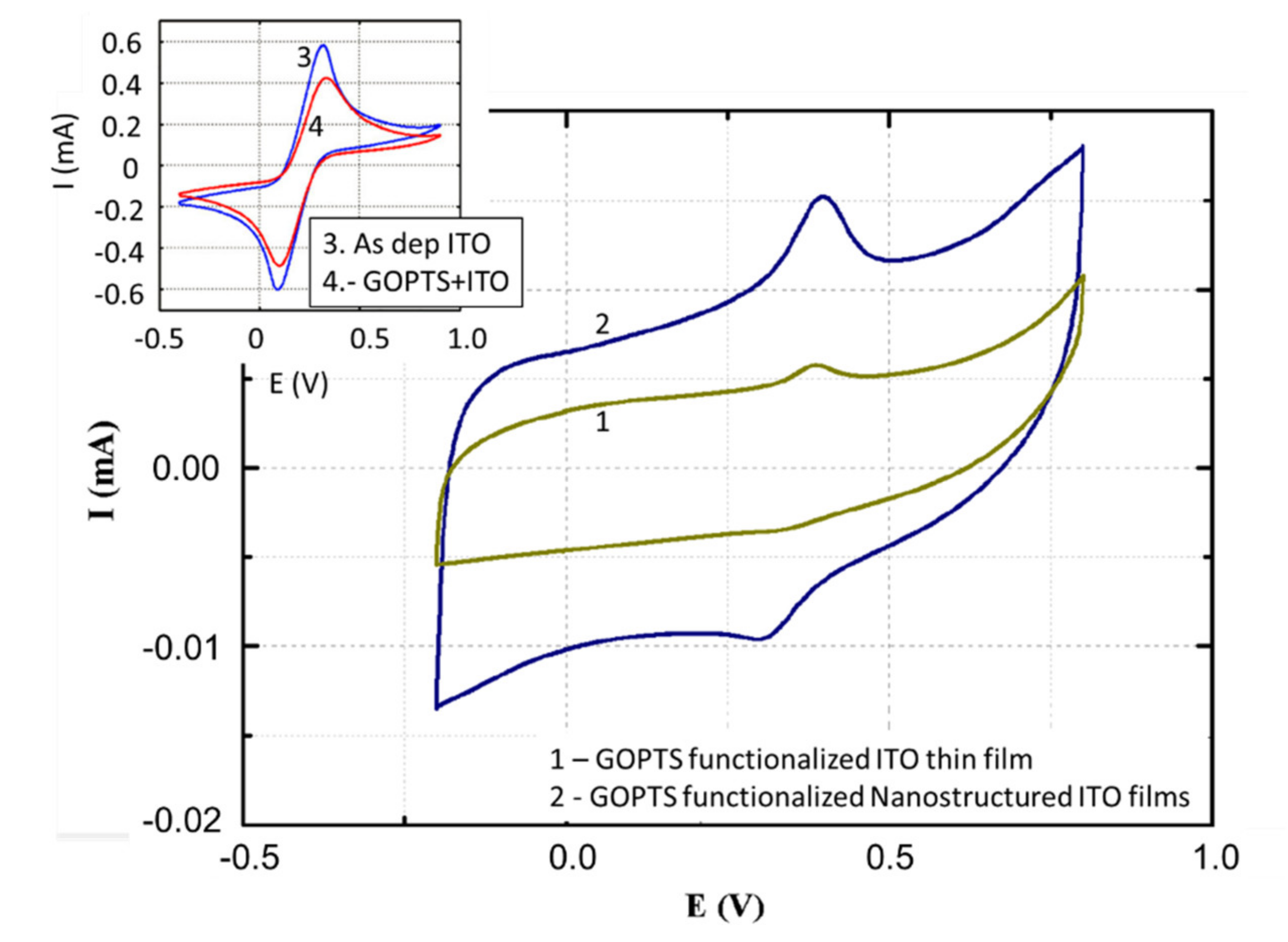
4. Electrochemical Characterization of the Functionalized Surface. Analysis of the Behavior of the Nanostructured vs Thin-Film ITO Working Electrodes
5. Discussion
6. Conclusions
Supplementary Materials
Author Contributions
Funding
Acknowledgments
Conflicts of Interest
References
- Logothetidis, S. (Ed.) Nanostructured Materials and Their Applications; Springer: Cham, Switzerland, 2012; ISBN 978-642-22227-6. [Google Scholar]
- Hussain, C.M. (Ed.) Handbook of Nanomaterials for Industrial Applications; Elsevier: Amsterdam, The Netherlands, 2018; ISBN 978-0-12-813351-4. [Google Scholar]
- Seehra, M. (Ed.) Nanostructured Materials, Fabrication to Applications; Interchopen: London, UK, 2017; ISBN 978-953-51-3372-8. [Google Scholar]
- Pruna, R. Transparent Nanostructured Metal Oxides for Chemical Bionsensors: Towards Point-of-Care Environments. Ph.D. Thesis, Universitat de Barcelona, Barcelona, Spain, 2019. [Google Scholar]
- Holzinger, M.; Le Goff, A.; Cosnier, S. Nanomaterials for biosensing applications: A review. Front. Chem. 2014, 2, 1–10. [Google Scholar] [CrossRef] [PubMed]
- Hou, S.; Zhang, A.; Su, M. Nanomaterials for Biosensing Applications. Nanomaterials 2016, 6, 58. [Google Scholar] [CrossRef] [PubMed]
- Canham, L.T. Silicon quantum wire array fabrication by electrochemical and chemical disolution of wafers. Appl. Phys. Lett. 1990, 57, 1046. [Google Scholar] [CrossRef]
- Poerschke, R.; Madelung, O. Data in Science and Techology: Semiconductors: Group IV Elementes and III-V Compounts; Springer: Berlin, Germany, 1991. [Google Scholar]
- Cullis, A.G.; Canham, L.T.; Calcott, P.D.J. The structural and luminescence properties of porous silicon. J. Appl. Phys. 1997, 82, 909–965. [Google Scholar] [CrossRef]
- Dancil, K.-P.S.; Greiner, D.P.; Sailor, M.J. A Porous Silicon Optical Biosensor: Detection of Reversible Binding of IgG to a Protein A-Modified Surface. J. Am. Chem. Soc. 1999, 121, 7925–7930. [Google Scholar] [CrossRef]
- Rivas, G.; Rubianes, M.; Rodriguez, M.; Ferreyra, N.; Luque, G.L.; Pedano, M.; Miscoria, S.; Parrado, C. Carbon nanotubes for electrochemical biosensing. Talanta 2007, 74, 291–307. [Google Scholar] [CrossRef]
- Yang, N.; Zhuang, H.; Hoffmann, R.; Smirnov, W.; Hees, J.; Jiang, X.; Nebel, C.E. Nanocrystalline 3C-SiC Electrode for Biosensing Applications. Anal. Chem. 2011, 83, 5827–5830. [Google Scholar] [CrossRef] [PubMed]
- Silicon-Germanium (SiGe) Nanostructures: Production, Properties and Applications in Electronics; Yasuhiro, S., Noritaka, U., Eds.; Woodhead Publishing in Materials: Cambridge, UK, 2011; ISBN 978-84569-689-4. [Google Scholar]
- Wang, H.W.; Ting, C.F.; Hung, M.K.; Chiou, C.H.; Liu, Y.L.; Liu, Z.; Ratinac, K.R.; Ringer, S.P. Three-dimensional electrodes for dye-sensitized solar cells: Synthesis of indium-tin-oxide nanowire arrays and ITO/TiO2 core-shell nanowire arrays by electrophoretic deposition. Nanotechnology 2009, 20, 55601. [Google Scholar] [CrossRef][Green Version]
- Choi, C.K.; Kihm, K.D.; English, A.E. Optoelectric biosensor using indium–tin–oxide electrodes. Opt. Lett. 2007, 32, 1405–1407. [Google Scholar] [CrossRef]
- Choi, C.K.; Margraves, C.H.; Jun, S.I.; English, A.E.; Rack, P.D.; Kihm, K.D. Opto-Electric Cellular Biosensor Using Optically Transparent Indium Tin Oxide (ITO) Electrodes. Sensors 2008, 8, 3257–3270. [Google Scholar] [CrossRef]
- Granqvist, C.G.; Hultåker, A. Transparent and conducting ITO films: New developments and applications. Thin Solid Film. 2002, 411, 1–5. [Google Scholar] [CrossRef]
- Hartnagel, H.; Dawar, A.L.; Jain, A.K.; Jagadish, C. Semiconducting Transparent Thin Films; Institute of Physics: Bristol, UK, 1995. [Google Scholar]
- Eshaghi, A.; Graeli, A. Optical and electrical properties of indium tin oxide (ITO) nanostructured thin films deposited on polycarbonate substrates “thickness effect”. Optik 2014, 125, 1478–1481. [Google Scholar] [CrossRef]
- Utsumi, K.; Matsunaga, O.; Takahata, T. Low resistivity ITO film prepared using the ultra high density ITO target. Thin Solid Film. 1998, 334, 330–340. [Google Scholar] [CrossRef]
- Patel, N.; Patel, P.; Vaishnav, V. Indium tin oxide (ITO) thin film gas sensor for detection of methanol at room temperature. Sens. Actuators B Chem. 2003, 96, 180–189. [Google Scholar] [CrossRef]
- Limmer, S.J.; Takahashi, K.; Cao, G. Electrochromic and transparent conducting oxide nanorods. Proc. SPIE 2003, 25. [Google Scholar] [CrossRef]
- George, J.; Menon, C. Electrical and optical properties of electron beam evaporated ITO thin films. Surf. Coat. Technol. 2000, 132, 45–48. [Google Scholar] [CrossRef]
- Bowden, E.F.; Hawkridge, F.M.; Blount, H.N. Interfacial electrochemistry of cytochrome c at tin oxide, indium oxide and platinum electrodes. J. Am. Chem. Soc. 1982, 104, 7641–7650. [Google Scholar] [CrossRef]
- Optically Transparent ITO Screen-Printed Electrode, (ref.ITO10), Dimensions: 33 × 10 × 0.175 mm. Available online: http://dropsens.com/en/screen_printed_electrodes_pag.html (accessed on 1 August 2020).
- Pruna, R.; Palacio, F.; López, M.; Blázquez, O.; Hernández, S.; Garrido, B.; Pérez, J.; Mir, M. Nanostructured ITO films for sensing applications. App. Phys. Lett. 2016, 109, 063109. [Google Scholar] [CrossRef]
- Huang, J.H.; Hsu, M.H.; Hsiao, Y.S.; Chen, P.; Yu, P.; Chu, C.W. Performance of chromophore-type electrochromic devices employing indium tin oxide nanorod optical amplification. Sol. Energy Mater. Sol. Cells 2012, 98, 191. [Google Scholar] [CrossRef]
- Pan, C.L.; Yand, C.H.; Pan, R.P.; Yu, P.; Lin, G.R. Nanostructured Indium Tin Oxies and Other Transparent Conducting Oxides: Characteristics and Applications in the THz Frequency Range. In Terahertz Spectroscopy—A Cutting Edge Technology; Uddin, J., Ed.; IntechOpen: London, UK, 2017; ISBN 978-953-51-3032-1. [Google Scholar]
- Wang, Z.; Zhang, Z. Electron Beam Evaporation Deposition. In Advanced Nanodeposition Methods; Chen, X., Lin, Y., Eds.; Wiley & Sons: Hoboken, NJ, USA, 2016; ISBN 9783527340255. [Google Scholar]
- Pan, T. Carbon Nanomaterials and 2D layered materials development by Chemical Vapor Deposition. In Advanced Nanodeposition Methods; Chen, X., Lin, Y., Eds.; Wiley & Sons: Hoboken, NJ, USA, 2016. [Google Scholar]
- Yang, W. Nanostructures and thin film deposited with sputtering. In Advanced Nanodeposition Methods; Chen, X., Lin, Y., Eds.; Wiley & Sons: Hoboken, NJ, USA, 2016. [Google Scholar]
- Chen, X.; Zhou, W.; Xie, D.; Cao, H. Nanomaterial Development Using In Situ Liquid Cell Transmission Electron Microscopy. In Advanced Nanodeposition Methods; Chen, X., Lin, Y., Eds.; Wiley & Sons: Hoboken, NJ, USA, 2016. [Google Scholar]
- Zhang, H. Nanostructures Development with Atomic Layer Deposition. In Advanced Nanodeposition Methods; Chen, X., Lin, Y., Eds.; Wiley & Sons: Hoboken, NJ, USA, 2016. [Google Scholar]
- Pruna, R.; López, M.; Teixidor, F. Tuning the deposition parameters for optimizing the faradaic and non-faradaic electrochemical performance of nanowire array-shaped ITO electrodes prepared by electron beam evaporation. Nanoscale 2019, 11, 276–284. [Google Scholar] [CrossRef]
- Kumar, R.R.; Rao, K.N.; Rajanna, K.; Phani, A.R.; Rajaboina, R.K. Low temperature and self catalytic growth of ultrafine ITO nanowires by electron beam evaporation method and their optical and electrical properties. Mater. Res. Bull. 2014, 52, 167–176. [Google Scholar] [CrossRef]
- Maruyana, T.; Fukui, K. Indium-tin oxide thin films prepared by chemical vapor deposition. J. Appl. Phys. 1991, 70, 3848–3851. [Google Scholar] [CrossRef]
- DigitalMicrograph Scripts. Available online: https://www.gatan.com/resources/digitalmicrograph-scripts (accessed on 1 August 2020).
- Mitchell, D.; Schaffer, B. Scripting-customised microscopy tools for Digital Micrograph™. Ultramicroscopy 2005, 103, 319–332. [Google Scholar] [CrossRef] [PubMed]
- Fung, M.K.; Sun, Y.C.; Ng, A.M.C.; Chen, X.Y.; Wong, K.K.; Djurišić, A.B.; Chan, W.K. Indium tin oxide nanowires growth by dc sputtering. Appl. Phys. A 2011, 104, 1075–1080. [Google Scholar] [CrossRef]
- Johnson, M.C.; Aloni, S.; McCready, D.E.; Bourret-Courchesne, E.D. Controlled vapor-liquid-solid growth of indium, gallium and tin oxide nanowires via chemical vapor deposition. Cris. Growth Des. 2006, 6, 1936. [Google Scholar] [CrossRef]
- Yu, H.K.; Dong, W.J.; Jung, G.H.; Lee, J.-L. Three-Dimensional Nanobranched Indium–Tin-Oxide Anode for Organic Solar Cells. Acs Nano 2011, 5, 8026–8032. [Google Scholar] [CrossRef] [PubMed]
- Meng, G.; Yanagida, T.; Nagashima, K.; Yoshida, H.; Kanai, M.; Klamchuen, A.; Zhuge, F.; He, Y.; Rahong, S.; Fang, X.; et al. Impact of Preferential Indium Nucleation on Electrical Conductivity of Vapor–Liquid–Solid Grown Indium–Tin Oxide Nanowires. J. Am. Chem. Soc. 2013, 135, 7033. [Google Scholar] [CrossRef] [PubMed]
- Yu, H.K.; Lee, J.-L. Growth mechanism of metal-oxide nanowires synthesized by electron beam evaporation: A self-catalytic vapor-liquid-solid process. Sci. Rep. 2014, 4, 6589. [Google Scholar] [CrossRef] [PubMed]
- Beaudry, A.L.; Tucker, R.T.; LaForge, J.M.; Taschuk, M.T.; Brett, M.J. Indium tin oxide nanowhisker morphology control by vapour–liquid–solid glancing angle deposition. Nanotechnology 2012, 23, 105608. [Google Scholar] [CrossRef] [PubMed]
- Yamamoto, N.; Morisawa, K.; Murakami, J.; Nakatani, Y. Formation of ITO Nanowires Using Conventional Magnetron Sputtering. Ecs Solid State Lett. 2014, 3, P84–P86. [Google Scholar] [CrossRef]
- Li, Q.; Yun, F.; Li, Y.; Ding, W.; Zhang, Y. Fabrication and application of indium-tin-oxide nanowire networks by polystyrene-assisted growth. Sci. Rep. 2017, 7, 1600. [Google Scholar] [CrossRef] [PubMed]
- Gale, W.F.; Totemeier, T.C. Smithells Metals Reference, 8th ed.; Elsevier: Amsterdam, The Netherlands, 2004. [Google Scholar]
- Yong, T.-K.; Tan, S.-S.; Nee, C.-H.; Yap, S.-S.; Kee, Y.-Y.; Sáfrán, G.; Horváth, Z.E.; Moscatello, J.; Yap, Y.K.; Tou, T.-Y. Pulsed laser deposition of indium tin oxide nanowires in argon and helium. Mater. Lett. 2012, 66, 280–281. [Google Scholar] [CrossRef]
- Van Dijken, J.G.; Brett, M.J. Nanopillar ITO electrodes via argon plasma etching. J. Vac. Sci. Technol. A 2012, 30, 40606. [Google Scholar] [CrossRef]
- O’Dwyer, C.; Szachowicz, M.; Visimberga, G.; Lavayen, V.; Newcomb, S.B.; Sotomayor-Torres, C.M. Bottom-up growth of fully transparent contact layers of indium tin oxide nanowires for light-emitting devices. Nat. Nanotechnol. 2009, 4, 239–244. [Google Scholar] [CrossRef]
- Baskaran, A.; Smereka, P. Mechanisms of Stranski-Krastanov growth, J. Appl. Phys. 2012, 111, 044321. [Google Scholar] [CrossRef]
- Elfallal, I.; Pilkington, R.; Hill, A. Formulation of a statistical thermodynamic model for the electron concentration in heavily doped metal oxide semiconductors applied to the tin-doped indium oxide system. Thin Solid Film. 1993, 223, 303–310. [Google Scholar] [CrossRef]
- Schmidt, V.; Senz, S.; Gösele, U. The shape of epitaxially grown silicon nanowires and the influence of line tension. Appl. Phys. A 2005, 80, 445–450. [Google Scholar] [CrossRef]
- Schmidt, V.; Wittemann, J.V.; Gosele, U. Growth, thermodynamics and electrical properties of silicon nanowires. Chem. Rev. 2010, 110, 361–388. [Google Scholar] [CrossRef]
- Agnihotry, S.A.; Saini, K.K.; Saxena, T.K.; Nagpal, K.C.; Chandra, S. Studies on e-beam deposited transparent conductive lms of in2o3: Sn at moderate substrate temperatures. J. Phys. D Appl. Phys. 1985, 18, 2087. [Google Scholar] [CrossRef]
- Senthilkumar, V.; Vickraman, P.; Jayachandran, M.; Sanjeeviraja, C. Structural and optical properties of indium tin oxide (ITO) thin films with different compositions prepared by electron beam evaporation. Vacuum 2010, 84, 864–869. [Google Scholar] [CrossRef]
- Dubrovskii, V.G.; Sibirev, N.V. General form of the dependences of nanowire growth rate on the nanowire radius. J. Cryst. Growth 2007, 304, 504–513. [Google Scholar] [CrossRef]
- Bard, A.J.; Faulkner, L.R. Electrochemical Methods: Fundamentals and Applications; Wiley & Sons: New York, NY, USA, 1980; Volume 2. [Google Scholar]
- Gau, V.; Ma, S.-C.; Wang, H.; Tsukuda, J.; Kibler, J.; Haake, D.A. Electrochemical molecular analysis without nucleic acid amplification. Methods 2005, 37, 73–83. [Google Scholar] [CrossRef] [PubMed]
- Myland, C.; Oldham, K.B. An analytical expression for the current-voltage relationship during reversible cyclic voltammetry. J. Electroanal. Chem. 1983. [Google Scholar] [CrossRef]
- Park, J.H.; Park, H.K.; Jeong, J.; Kim, W.; Min, B.K.; Do, Y.R. Wafer-Scale Growth of ITO Nanorods by Radio Frequency Magnetron Sputtering Deposition. J. Electrochem. Soc. 2011, 158, K131. [Google Scholar] [CrossRef]
- Lee, C.-T.; Yu, Q.-X.; Tang, B.-T.; Lee, H.-Y. Effects of plasma treatment on the electrical and optical properties of indium tin oxide films fabricated by r.f. reactive sputtering. Thin Solid Film. 2001, 386, 105–110. [Google Scholar] [CrossRef]
- Pruna, R.; Baraket, A.; Bonhommé, A.; Zine, N.; Errachid, A.; López, M. Novel nanostructured indium tin oxide electrode for electrochemical immunosensors: Suitability for the detection of TNF-α. Electrochim. Acta 2018, 283, 1632–1639. [Google Scholar] [CrossRef]
- Pruna, R.; Palacio, F.; Martínez, M.; Blázquez, O.; Hernández, S.; Garrido, B.; López, M. Organosilane-functionalization of nanostructured indium tin oxide films. Interface Focus 2016, 6, 20160056. [Google Scholar] [CrossRef]
- Materne, T.; de Buyl, F.; Witucki, G.L. Organosilane Technology in Coating Applications: Review and Perspectives; Dow Corning Corp: Midland, MI, USA, 2012. [Google Scholar]
- Manifacier, J.C. Thin metallic oxides as transparent conductors. Thin Solid Film. 1982, 90, 297–308. [Google Scholar] [CrossRef]


| Temperature (°C) | 100 | 200 | 300 | 400 | 500 |
|---|---|---|---|---|---|
| Mean Nanowire Diameter (nm) | No NW | 33.56 | 34.98 | 36.29 | 40.91 |
| STDV Diameter (nm) | 2.266 | 2.955 | 3.736 | 6.439 | |
| Mean Length (nm) | No NW | 72.23 | 124.6 | 135 | 457.95 |
| STDV Length (nm) | 13.13 | 21.95 | 32.01 | 135.8 | |
| Number of Nanowires/Area Unit | - | 433 nw/µm2 | 610 nw/µm2 | 625 nw/µm2 | 616 nw/µm2 |
| Nanowire Area vs. Total Area | - | 77.7% | 95.4% | 97.8% | 96.66% |
| Mean Distance Between Nanowires (nm) | - | 0.24 | In contact | In contact | In contact |
| Exposed Time (min) | Mean Length (nm) | STDV Length (nm) | Mean Diameter (nm) | STDV Diameter (nm) |
|---|---|---|---|---|
| 10 | 86.98 | 19.62 | 19.95 | 2.139 |
| 12 | 123.7 | 39.08 | 19.7 | 2.735 |
| 14 | 153 | 28.19 | 22.59 | 5.783 |
| 15 | 211 | 58.72 | 24.71 | 4.331 |
| 20 | 233.1 | 44.59 | 24.95 | 3.715 |
| 25 | 365.7 | 101.3 | 28.03 | 7.322 |
| 30 | 439.4 | 77.5 | 31.23 | 10.231 |
| Sample (°C) | Area (cm2) | Transmittance (%) @600 nm | Sheet Resistance (Ω/sq) |
|---|---|---|---|
| 200 | 0.31 | 79 | 215 |
| 300 | 0.42 | 82 | 105 |
| 400 | 0.38 | 81 | 155 |
| 500 | 0.40 | 82 | 145 |
| Composition In/Sn wt.% | Active Area (cm2) |
|---|---|
| 90/10 | 0.623 ± 0.017 |
| 80/20 | 0.273 ± 0.012 |
| 70/30 | 0.1 ± 0.012 |
| 60/40 | Not detected |
| Thin film (reference) | 0.029 ± 0.004 |
| O1s Peak (%) | Si2p Peak (%) | O Peak1 Position (eV) | O Std. Dev.1 (eV) | O Peak2 Position (eV) | O Std. Dev. 2 (eV) | Si Peak Position (eV) | Si Std. Dev. (eV) | |
|---|---|---|---|---|---|---|---|---|
| Bare ITO | 51 | 0.5 | 531.2 | 1.70 | 530 | 0.84 | 101.3 | 1 |
| GOPTS Func. ITO | 58.1 | 7 | 532.4 | 1.35 | 530.1 | 0.97 | 102.4 | 1.21 |
© 2020 by the authors. Licensee MDPI, Basel, Switzerland. This article is an open access article distributed under the terms and conditions of the Creative Commons Attribution (CC BY) license (http://creativecommons.org/licenses/by/4.0/).
Share and Cite
López, M.; Frieiro, J.L.; Nuez-Martínez, M.; Pedemonte, M.; Palacio, F.; Teixidor, F. Nanostructure ITO and Get More of It. Better Performance at Lower Cost. Nanomaterials 2020, 10, 1974. https://doi.org/10.3390/nano10101974
López M, Frieiro JL, Nuez-Martínez M, Pedemonte M, Palacio F, Teixidor F. Nanostructure ITO and Get More of It. Better Performance at Lower Cost. Nanomaterials. 2020; 10(10):1974. https://doi.org/10.3390/nano10101974
Chicago/Turabian StyleLópez, Manel, Juan Luis Frieiro, Miquel Nuez-Martínez, Martí Pedemonte, Francisco Palacio, and Francesc Teixidor. 2020. "Nanostructure ITO and Get More of It. Better Performance at Lower Cost" Nanomaterials 10, no. 10: 1974. https://doi.org/10.3390/nano10101974
APA StyleLópez, M., Frieiro, J. L., Nuez-Martínez, M., Pedemonte, M., Palacio, F., & Teixidor, F. (2020). Nanostructure ITO and Get More of It. Better Performance at Lower Cost. Nanomaterials, 10(10), 1974. https://doi.org/10.3390/nano10101974