Article

Steep Subthreshold Swing and Enhanced Illumination Stability InGaZnO Thin-Film Transistor by Plasma Oxidation on Silicon Nitride Gate Dielectric

State Key Laboratory of Integrated Optoelectronics, College of Electronic Science and Engineering, Jilin University, Changchun 130012, China
*
Author to whom correspondence should be addressed.
Membranes 2021, 11(11), 902; https://doi.org/10.3390/membranes11110902
Submission received: 19 October 2021 / Revised: 10 November 2021 / Accepted: 12 November 2021 / Published: 22 November 2021
(This article belongs to the Special Issue Thin-Film Transistors)

Abstract

:
In this paper, an InGaZnO thin-film transistor (TFT) based on plasma oxidation of silicon nitride (SiNx) gate dielectric with small subthreshold swing (SS) and enhanced stability under negative bias illumination stress (NBIS) have been investigated in detail. The mechanism of the high-performance InGaZnO TFT with plasma-oxidized SiNx gate dielectric was also explored. The X-ray photoelectron spectroscopy (XPS) results confirmed that an oxygen-rich layer formed on the surface of the SiNx layer and the amount of oxygen vacancy near the interface between SiNx and InGaZnO layer was suppressed via pre-implanted oxygen on SiNx gate dielectric before deposition of the InGaZnO channel layer. Moreover, the conductance method was employed to directly extract the density of the interface trap (Dit) in InGaZnO TFT to verify the reduction in oxygen vacancy after plasma oxidation. The proposed InGaZnO TFT with plasma oxidation exhibited a field-effect mobility of 16.46 cm2/V·s, threshold voltage (Vth) of −0.10 V, Ion/Ioff over 108, SS of 97 mV/decade, and Vth shift of −0.37 V after NBIS. The plasma oxidation on SiNx gate dielectric provides a novel approach for suppressing the interface trap for high-performance InGaZnO TFT.

1. Introduction

In recent decades, InGaZnO based oxide TFTs have been widely investigated to compete with conventional silicon-based TFTs for active matrix organic light-emitting display (AMOLED) due to its advantages of high field-effect mobility [1], excellent uniformity for large-scaled display panels [2], and high optical transparency in the visible spectrum [3]. Moreover, the InGaZnO shows great penitential for the application of flexible electronic devices owing to its insensitive to intrinsically distorted metal–oxygen–metal chemical bonds [4] and low-temperature fabrication process [5,6,7]. To investigate the further potential for advanced electronic applications such as high refresh rate display and low power consuming devices, the field-effect mobility, stability, and SS should be critically considered. Among the strategies of boosting the performance of InGaZnO TFTs, the modification of interface between InGaZnO and gate dielectric is one of the effective ways [8,9,10]. The plasma treatment technique has been widely applied to tailor the surface properties of semiconductors [11,12]. Additionally, the interface between the post-deposited thin film and the former layer could also be affected by plasma treatment. In this work, the plasma oxidation on SiNx gate dielectric for InGaZnO TFT with fairly low SS and excellent illumination stability has been reported. The effect of plasma oxidation on the electrical characteristic, interface trap density, and chemical component for InGaZnO have been investigated in detail. The proposed plasma oxidation method on SiNx gate dielectric provides a novel approach for achieving the high-performance InGaZnO TFT.

2. Materials and Methods
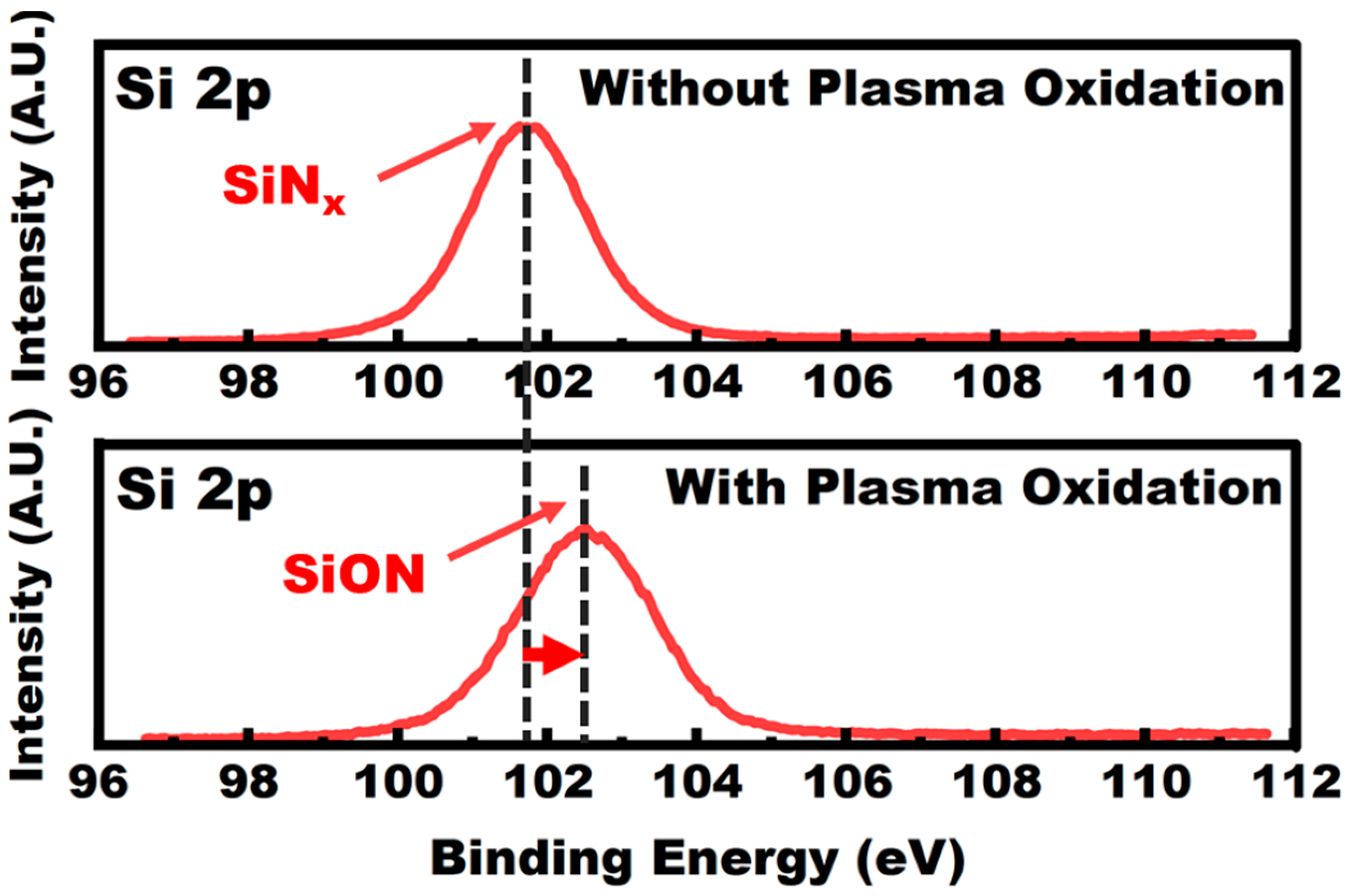
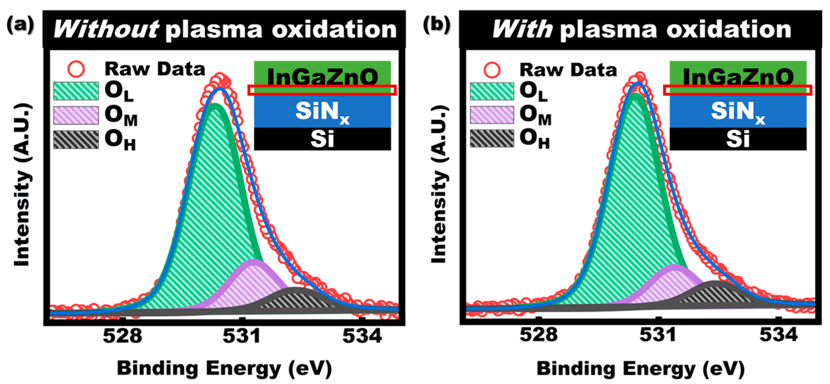
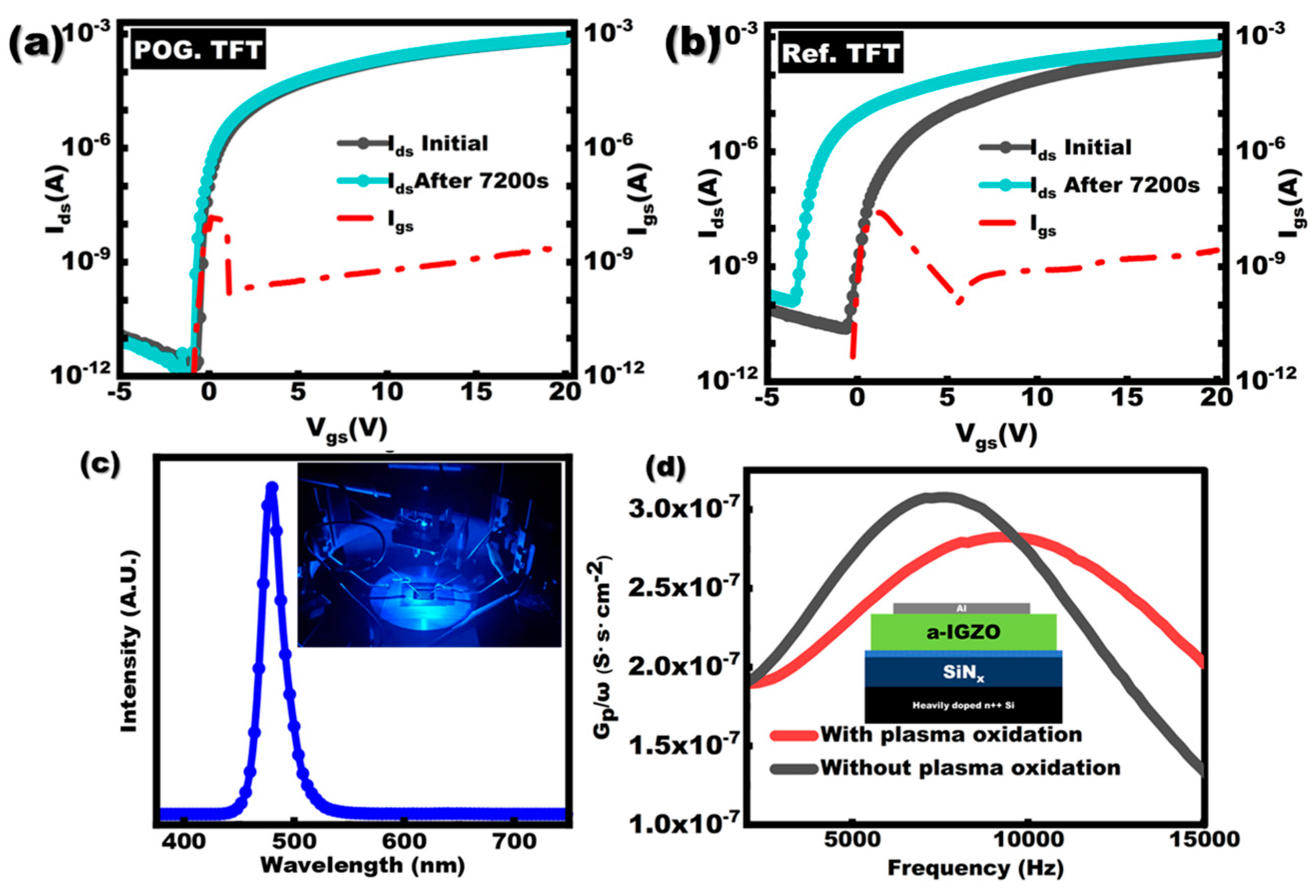
The InGaZnO TFT was fabricated on the 210 nm-thickness SiNx gate dielectric with heavily n-doped (As) Si as a gate electrode. The SiNx layer was deposited by low-pressure chemical vapor deposition at the pressure of 160 mTorr from NH3 and SiCl2H2 precursor with the gas flow of 40 sccm and 175 sccm, respectively. The as-deposit SiNx layer was treated in the oxygen plasma for 60 s. The oxygen plasma was generated by the capacity coupling configuration via a radio frequency power supply (Seren, R301) and matching box with a fixed power of 40 W under DC bias about 180 V at a constant pressure of 5 mTorr. The whole substrate was rotated at 5 revolutions per minute to keep the uniformity during the whole plasma oxidation process. Afterwards, a 30 nm thick InGaZnO channel layer was deposited by magnetron sputtering from an InGaZnO target (1:1:1 at%) with a power of 200 W in the same chamber without exposure to the atmosphere. Then, the source/drain electrodes were thermal evaporated Al metal via the shadow mask process with a channel length (L) of 100 μm and width (W) of 1000 μm, respectively. Finally, the InGaZnO TFT with plasma oxidation SiNx gate dielectric (hereinafter referred to as ‘POG. TFT’) was post-annealed at 250 °C in air for 1 h. The reference sample (hereinafter referred to as ‘Ref. TFT’) was with the same fabrication sequence except for plasma oxidation on SiNx dielectric. The process flow diagram and structure of InGaZnO TFTs in this work are shown in Figure 1. The electronic characteristics were evaluated using a source-meter unit (2636B, Keithley, Beaverton, OR, USA) and an LCR meter (IM3536, Hioki, Japan). The chemical status of the thin films was analyzed by XPS (Nexsa, Thermo Scientific, Waltham, MA, USA) with all the XPS data calibrated by C1s BE at 284.8 eV. Surface morphology was performed by the atomic force microscope (AFM, Dimension Icon, Bruker, Billerica, Germany).

3. Results

Figure 2a shows the transfer characteristics at Vds = 10 V while the Vgs was swept from −5 V to 20 V with a step of 0.125 V for POG. TFT and Ref. TFT.
The field-effect mobility in saturation region is extracted from the following equation:
μ F E = 2 L / W C o x ( d I d s / d V g s ) 2
and the SS is calculated by [13]:
S S = m i n ( d V g s / d l o g I d s )  
where Cox, L, W, Ids, and Vgs are the gate capacitance per unit area, channel length, channel width, current of drain to source, and gate bias voltage, respectively. All the extracted parameters are summarized in Table 1.
Compared with the Ref. TFT, the mobility of POG. TFT increased from 10.64 cm2/V·s to 16.46 cm2/V·s and the Vth slightly shifted from 1.95 V to −0.10 V. The SS has an obvious decrease from 312 mV/decade to 97 mV/decade. Generally, the value of SS is dominated by the density of trap state in semiconductor bulk and interface trap between semiconductor and gate dielectric. The roughness of the gate dielectric could directly influence the interface between the InGaZnO and dielectric [14,15,16]. Hence, to investigate the condition of the interface, the AFM topography was obtained for the SiNx sample with/without plasma oxidation under the identical process condition as described before, as shown in Figure 2b,c. The value of the surface roughness is decreased from 1.23 nm to 0.95 nm after plasma oxidation. The large cluster SiNx or absorbed carbon contaminant could be partly peered off from the surface of the SiNx by the plasma bombardment which provides a smoother surface for the following sputtering of InGaZnO. Different from using electron cyclotron resonance (ECR) remote plasma to treat the thin film [17], capacitive coupling was used to provide O2 plasma with a stronger bombardment effect to treat SiNx insulators. These strongly bombarded O2 plasmas would treat the SiNx insulators more adequately. To further verify the impact on elements composition after plasma oxidation, the elements composition by XPS for the surface of SiNx thin film without/with plasma oxidation is shown in Figure 2d. For the sample of SiNx without plasma oxidation, the oxygen atoms are mainly attributed to the surface absorbed oxygen from the environment on the surface of SiNx. After plasma oxidation, the O atoms ratio increased from 25.0% to 38.2%, the Si-O bonding would be formed on the surface of SiNx thin film. To verify this speculation, the XPS spectra of the Si2p in the surface of SiNx thin film were also measured. As shown in Figure 3, the Si2p binding energy on the surface of SiNx at 102.5 eV (with plasma oxidation). This binding energy of Si2p is between those of the Si3N4 (101.7 eV) and SiO2 (103.5 eV), which indicate the formation of Si-O bonding on the surface of SiNx thin film with plasma oxidation. Since the SiNx thin film was mounted on the anode of the plasma generator in this work, an electric field point to the substrate could form on the SiNx surface. As a result, the cations in the plasma such as O2+ or O+ could sustain surface bombardment, which causes the Si-N bonds to break and oxygen atoms could substitute partly nitrogen atoms to form an oxygen-rich layer on the SiNx surface. In addition, the carbon atoms ratio has also been reduced after plasma treatment. Such carbon is mainly induced by the inevitable contamination from the vacuum chamber or transfer process. Since the carbon has been reported as an electron trap in InGaZnO [18], the reduction of carbon on the SiNx surface could also increase the mobility and meliorate the SS of the InGaZnO TFT.
Furthermore, the influence of SiNx surface plasma oxidation on the post-deposit InGaZnO layer was evaluated by the O1s XPS profile at the interface between SiNx and InGaZnO for the sample of with/without plasma oxidation. Figure 4a,b shows the XPS spectra of the O1s core level in InGaZnO near the interface between SiNx and InGaZnO. The O1s peak of XPS spectra is deconvoluted into three peaks with a binding energy of about 530.3 eV, 531.3 eV, and 532.3 eV. The main peak centered at about 530 eV (OL) is related to the lattice oxygen. The peak centered at 531.3 eV (OM) and 532.3 eV (OH) is related to the oxygen vacancies and -OH hydroxide oxygen [19,20], respectively. The area ratio of OL:OM:OH for the sample without plasma oxidation and with oxidation is about 1:0.25:0.10 and 1:0.18:0.12, respectively. This result indicates that the amount of oxygen vacancies in a-InGaZnO near the interface between SiNx and InGaZnO is decreased after surface plasma oxidation of the SiNx layer. This phenomenon could be explained by the following mechanism. After InGaZnO layer deposition, the thermal post-anneal process could cause the oxygen atoms near the interface to diffuse from the InGaZnO layer into the SiNx layer, which is driven by the oxygen concentration gradient. Such a diffusion process could be partly restrained by reducing the concentration gradient via pre-implantation oxygen atoms at the SiNx surface leading to a reduction in oxygen vacancies in InGaZnO near the interface between SiNx and the InGaZnO layer. Since the oxygen vacancy is considered as the origin of the defects in InGaZnO [21,22], it could be deduced that the density of interface traps in InGaZnO TFTs after O2 plasma treatment should be decreased. On the other hand, the reduction in oxygen vacancy only near the interface between SiNx and the InGaZnO layer would not significantly decrease the carrier concentration in the InGaZnO layer. Hence, the SS should also be decreased and the mobility should be increased, which is consistent with the decrease in the extracted value of SS and the increase in mobility from transfer curves of TFTs in Table 1.
Since light illumination is inevitable during the display panel working, the NBIS test should be critically considered for InGaZnO TFTs. Furthermore, the result of NBIS could also reflect the interface status in InGaZnO TFT. Therefore, the NBIS tests were performed for both Ref. TFT and POG. TFT under a blue light-emitting diode (LED) illumination with a central wavelength of about 480 nm at full width at half maximum of 10 nm. The LED spectrum was assessed by a spectroradiometer (SpectraScan, PR-655), as shown in Figure 5c. Figure 5a,b represents the NBIS results for Ref. TFT and POG. TFT. The Vds and Vgs were fixed at 0 V and −10 V, respectively. The threshold voltage shift (ΔVth) after 7200 s NBIS is −4.75 V for Ref. TFT and dramatically decreased to −0.37 V for POG. TFT. During the NBIS test, the holes and electrons are generated by the light illumination, while the oxygen vacancy could act as the hole trap to capture the photoinduced holes which are likely to drift toward the channel/dielectric interface under negative gate bias, resulting in NBIS instability in InGaZnO TFTs [23,24]. Therefore, owing to the effective decrease in the amount of oxygen vacancies near the interface between InGaZnO and SiNx by plasma oxidation, the holes trapped by interfacial traps could also be reduced, resulting in a smaller ΔVth after NBIS.
To directly obtain the Dit between SiNx gate dielectric and the InGaZnO layer, the conductance method [25] was employed. This small-signal steady-state method has been widely used to analyze the properties of the interface trap owing to its accuracy and sensitivity in extracting the Dit. The Dit can be calculated from the equivalent parallel conductive (Gp) divided by ω from the following equation:
G p / ω = q ω τ i t D i t / [ 1 + ( ω τ i t ) 2 ]  
The Gp/ω can be directly calculated from the measured equivalent parallel conductance (Gm) and measured capacitance (Cm) by the following express:
G p / ω = ω G m C o x 2 / [ G m 2 + ω 2 ( C o x C m ) 2 ]  
where Cox is capacitor per unit area. At maximum Gp/ω, the ω is equal to 1/τit, the Dit can be expressed by the measured maximum conductance as:
D i t = 2 / q ( G p / ω ) m a x
Two metal-oxide-semiconductor (MOS) capacitors have been fabricated with a similar structure except for the plasma oxidation on the SiNx surface. The Gp/ω as a function of frequency is shown in Figure 5d. The inset is the structure of the MOS capacitor. The extracted Dit is 3.02 × 1012 cm−2·eV−1 and 1.45 × 1012 cm−2·eV−1 for Ref. MOS and POG. MOS capacitors, respectively. This result also proved that the interface traps at SiNx/InGaZnO are reduced by the SiNx surface plasma oxidation, which is consistent with the aforementioned XPS and NBIS results. Table 2 represents the performance metrics of InGaZnO TFT in this work and other reported SiNx-related InGaZnO TFTs. Among all SiNx-based InGaZnO TFTs, the TFT from our work exhibits a combination of high Ion/Ioff and the lowest SS.

4. Conclusions

In this work, we demonstrated an a-InGaZnO TFT with plasma oxidation SiNx gate dielectric. With plasma oxidation of SiNx gate dielectric, the SS and ΔVth under NBIS were significantly improved from 312 mV/decade to 97 mV/decade and −4.75 V to −0.37 V, respectively. The plasma oxidation on SiNx could provide a smoother surface and form an oxygen-rich layer at the SiNx/InGaZnO interface. The XPS result indicates that the amount of oxygen vacancy near the SiNx/InGaZnO interface was effectively reduced after plasma oxidation. Furthermore, the interface trap density has been extracted by conductance method, which shows a decrease from 3.02 × 1012 cm−2·eV−1 to 1.45 × 1012 cm−2·eV−1 after plasma oxidation. The plasma oxidation on SiNx gate dielectric in this work provides a potential approach for suppressing the interface trap in SiNx based InGaZnO TFT for an advanced electronic application.

Author Contributions

Conceptualization, Y.L. and C.L.; methodology, Y.L. and C.L.; software, Y.L. and C.L.; validation, C.P. and M.L.; formal analysis, Y.L., C.L., H.Q., M.L. and Z.C.; investigation, Y.L.; resources, Y.Z.; writing—original draft preparation, Y.L. and C.L.; writing—review and editing, Y.L. and Y.Z.; supervision, Y.Z. All authors have read and agreed to the published version of the manuscript.

Funding

This research was funded by National Natural Science Foundation of China, grant number 61675089.

Institutional Review Board Statement

Not applicable.

Informed Consent Statement

Not applicable.

Data Availability Statement

Data are contained within the article.

Acknowledgments

Dehui Li is appreciated for the technical support.

Conflicts of Interest

The authors declare no conflict of interest.

References

  1. Lee, J.S.; Chang, S.; Koo, S.-M.; Lee, S.Y. High-Performance InGaZnO TFT with ZrO2 Gate Dielectric Fabricated at Room Temperature. IEEE Electron Device Lett. 2010, 31, 225–227. [Google Scholar] [CrossRef]
  2. Jariwala, D.; Sangwan, V.K.; Seo, J.-W.T.; Xu, W.C.; Smith, J.; Kim, C.H.; Lauhon, L.J.; Marks, T.J.; Hersam, M.C. Large-Area, Low-Voltage, Antiambipolar Heterojunctions from Solution-Processed Semiconductors. Nano Lett. 2015, 15, 416–421. [Google Scholar] [CrossRef] [PubMed] [Green Version]
  3. Wang, Y.; Liu, S.W.; Sun, X.W.; Zhao, J.L.; Goh, G.K.L.; Vu, Q.V.; Yu, H.Y. Highly transparent solution processed In-Ga-Zn oxide thin films and thin film transistors. J. Sol.-Gel. Sci. Technol. 2010, 55, 322–327. [Google Scholar] [CrossRef]
  4. Nomura, K.; Ohta, H.; Takagi, A.; Kamiya, T.; Hirano, M.; Hosono, H. Room-temperature fabrication of transparent flexible thin-film transistors using amorphous oxide semiconductors. Nature 2004, 432, 488–492. [Google Scholar] [CrossRef] [PubMed]
  5. Yabuta, H.; Sano, M.; Abe, K.; Aiba, T.; Den, T.; Kumomi, H. High-mobility thin-film transistor with amorphous InGaZnO4 channel fabricated by room temperature rf-magnetron sputtering. Appl. Phys. Lett. 2006, 89, 112123. [Google Scholar] [CrossRef]
  6. Chiu, C.J.; Chang, S.P.; Chang, S.J. High-Performance InGaZnO Thin-Film Transistor Using Ta2O5 Gate Dielectric. IEEE Electron. Device Lett. 2010, 31, 1245–1247. [Google Scholar] [CrossRef]
  7. Hsu, H.H.; Chang, C.Y.; Cheng, C.H. A Flexible IGZO Thin-Film Transistor with Stacked TiO2-Based Dielectrics Fabricated at Room Temperature. IEEE Electron. Device Lett. 2013, 34, 768–770. [Google Scholar] [CrossRef]
  8. Zheng, L.L.; Qian, S.B.; Wang, Y.H.; Liu, W.J.; Ding, S.J. Mobility and Stability Enhancement of Amorphous In-Ga-Zn-O TFTs with Atomic Layer Deposited Al2O3/SiO2 Stacked Insulators. IEEE J. Electron. Device 2016, 4, 347–352. [Google Scholar] [CrossRef]
  9. Abliz, A.; Wang, J.L.; Xu, L.; Wan, D.; Liao, L.; Ye, C.; Liu, C.S.; Jiang, C.Z.; Chen, H.P.; Guo, T.L. Boost up the electrical performance of InGaZnO thin film transistors by inserting an ultrathin InGaZnO:H layer. Appl. Phys. Lett. 2016, 108, 213501. [Google Scholar] [CrossRef]
  10. Lin, C.I.; Fang, Y.K.; Chang, W.C.; Chiou, M.W.; Chen, C.W. Effect of gate barrier and channel buffer layer on electric properties and transparence of the InGaZnO thin film transistor. Microelectron. Reliab. 2014, 54, 905–910. [Google Scholar] [CrossRef]
  11. Januar, M.; Prakoso, S.P.; Lan, S.Y.; Mahanty, R.K.; Kuo, S.Y.; Liu, K.C. The role of oxygen plasma in the formation of oxygen defects in HfOx films deposited at room temperature. J. Mater. Chem. C 2015, 3, 4104–4114. [Google Scholar] [CrossRef]
  12. Pu, H.F.; Zhou, Q.F.; Yue, L.; Zhang, Q. Investigation of oxygen plasma treatment on the device performance of solution-processed InGaZnO thin film transistors. Appl. Surf. Sci. 2013, 283, 722–726. [Google Scholar] [CrossRef]
  13. Kamiya, T.; Nomura, K.; Hosono, H. Present status of amorphous In–Ga–Zn–O thin-film transistors. Sci. Technol. Adv. Mater. 2010, 11, 044305. [Google Scholar] [CrossRef] [PubMed]
  14. Cho, Y.J.; Shin, J.H.; Bobade, S.M.; Kim, Y.B.; Choi, D.K. Evaluation of Y2O3 gate insulators for InGaZnO thin film transistors. Thin Solid Film 2009, 517, 4115–4118. [Google Scholar] [CrossRef]
  15. Syamala Rao, M.G.; Sánchez-Martinez, A.; Gutiérrez-Heredia, G.; Quevedo- López, M.A.; Ramírez-Bon, R. Sol-gel derived low temperature HfO2-GPTMS hybrid gate dielectric for InGaZnO thin-film transistors (TFTs). Ceram. Int. 2018, 44, 16428–16434. [Google Scholar] [CrossRef]
  16. Zou, X.; Fang, G.J.; Yuan, L.Y.; Tong, X.S.; Zhao, X.Z. Improved electrical characteristics and reliability of amorphous InGaZnO metal–insulator–semiconductor capacitor with high k HfOxNy gate dielectric. Microelectron. Reliab. 2010, 50, 954–958. [Google Scholar] [CrossRef]
  17. Moon, Y.-K.; Lee, S.; Kim, W.-S.; Kang, B.-W.; Jeong, C.-O.; Lee, D.-H.; Park, J.-W. Improvement in the bias stability of amorphous indium gallium zinc oxide thin-film transistors using an O2 plasma-treated insulator. Appl. Phys. Lett. 2009, 95, 013507. [Google Scholar] [CrossRef]
  18. Yoo, H.; Tak, Y.J.; Kim, W.-G.; Kim, Y.-G.; Kim, H.J. A selectively processible instant glue passivation layer for indium gallium zinc oxide thin-film transistors fabricated at low temperature. J. Mater. Chem. C 2018, 6, 6187–6193. [Google Scholar] [CrossRef]
  19. Kang, J.H.; Cho, E.N.; Kim, C.E.; Lee, M.-J.; Lee, S.J.; Myoung, J.-M.; Yun, I. Mobility enhancement in amorphous InGaZnO thin-film transistors by Ar plasma treatment. Appl. Phys. Lett. 2013, 102, 222103. [Google Scholar] [CrossRef] [Green Version]
  20. Zhang, P.P.; Samanta, S.; Fong, X.Y. Physical Insights into the Mobility Enhancement in Amorphous InGaZnO Thin-Film Transistor by SiO2 Passivation Layer. IEEE Trans. Electron Device Lett. 2020, 67, 2352–2357. [Google Scholar] [CrossRef]
  21. Korner, W.; Urban, D.F.; Elsasser, C. Origin of subgap states in amorphous In-Ga-Zn-O. J. Appl. Phys. 2013, 114, 163704. [Google Scholar] [CrossRef]
  22. Noh, H.-K.; Chang, K.J.; Ryu, B.; Lee, W.-J. Electronic structure of oxygen-vacancy defects in amorphous In-Ga-Zn-O semiconductors. Phys. Rev. B 2011, 84, 115205. [Google Scholar] [CrossRef]
  23. Ryu, B.; Noh, H.-K.; Choi, E.-A.; Chang, K.J. O-vacancy as the origin of negative bias illumination stress instability in amorphous In–Ga–Zn–O thin film transistors. Appl. Phys. Lett. 2010, 97, 022108. [Google Scholar] [CrossRef] [Green Version]
  24. Kim, J.H.; Kim, U.K.; Chung, Y.J.; Hwang, C.S. Correlation of the change in transfer characteristics with the interfacial trap densities of amorphous In–Ga–Zn–O thin film transistors under light illumination. Appl. Phys. Lett. 2011, 98, 232102. [Google Scholar] [CrossRef]
  25. Nicollian, E.H.; Brews, J.R. MOS (Metal Oxide Semiconductor) Physics and Technology; Wiley: New York, NY, USA, 1982. [Google Scholar]
  26. Jeong, C.-Y.; Lee, D.; Song, S.-H.; Cho, I.-T.; Lee, J.-H.; Cho, E.-S.; Kwon, H.-I. Border trap characterization in amorphous indium-gallium-zinc oxide thin-film transistors with SiOx and SiNx gate dielectrics. Appl. Phys. Lett. 2013, 103, 142104. [Google Scholar] [CrossRef]
  27. Han, K.-L.; Ok, K.-C.; Cho, H.-S.; Oh, S.; Park, J.-S. Effect of hydrogen on the device performance and stability characteristics of amorphous InGaZnO thin-film transistors with a SiO2/SiNx/SiO2 buffer. Appl. Phys. Lett. 2017, 111, 063502. [Google Scholar] [CrossRef]
  28. Ok, K.-C.; Park, S.H.K.; Hwang, C.-S.; Kim, H.; Shin, H.S.; Bae, J.; Park, J.-S. The effects of buffer layers on the performance and stability of flexible InGaZnO thin film transistors on polyimide substrates. Appl. Phys. Lett. 2004, 104, 063508. [Google Scholar] [CrossRef]
  29. Wang, R.Z.; Wu, S.L.; Jia, D.B.; Wei, Q.; Zhang, J.T. Influence of different conditions on the electrical performance of amorphous InGaZnO thin-film transistors with HfO2/SiNx stacked dielectrics. J. Vac. Sci. Technol. B 2017, 35, 051204. [Google Scholar] [CrossRef]
Figure 1. Process flow diagram and structure of InGaZnO TFT in this work.
Membranes 11 00902 g001
Figure 2. (a) Transfer characteristic curves for Ref. TFT and POG. TFT. The surface morphology for SiNx (b) without plasma oxidation and (c) with plasma oxidation. (d) The atomic ratio for the surface of SiNx thin film without/with plasma oxidation.
Membranes 11 00902 g002
Figure 3. Si2p XPS results on the surface SiNx film without and with plasma oxidation.
Membranes 11 00902 g003
Figure 4. XPS results for surface of SiNx thin film (a) without (b) with plasma oxidation.
Membranes 11 00902 g004
Figure 5. The curves of transfer characteristic before/after NBIS test for (a) Ref. TFT and (b) POG. TFT; (c) spectrum of blue LED used in NBIS test; (d) Gp/ω as the function of frequency for Ref. and POG. MOS capacitor.
Membranes 11 00902 g005
Table 1. Electrical parameters for InGaZnO TFT with/without SiNx surface plasma oxidation.
DeviceMobility (cm2/V·s)Vth (V)SS (mV/Decade)Ion/Ioff
Ref. TFT10.641.953121.68 × 107
POG. TFT16.46−0.10973.99 × 108
Table 2. Performance metrics of InGaZnO TFT in this work and other reported SiNx-related InGaZnO TFTs.
ReferenceMobility (cm2/V·s)Vth (V)SS (mV/decade)Ion/Ioff
This work16.46−0.10973.99 × 108
[26]10.92.04002 × 108
[27]8.790.811603 × 108
[28]14.43−1.25240
[29]18.13.41371.1 × 108
Publisher’s Note: MDPI stays neutral with regard to jurisdictional claims in published maps and institutional affiliations.

