Micro-LEDs, a Manufacturability Perspective


Abstract
1. Introduction
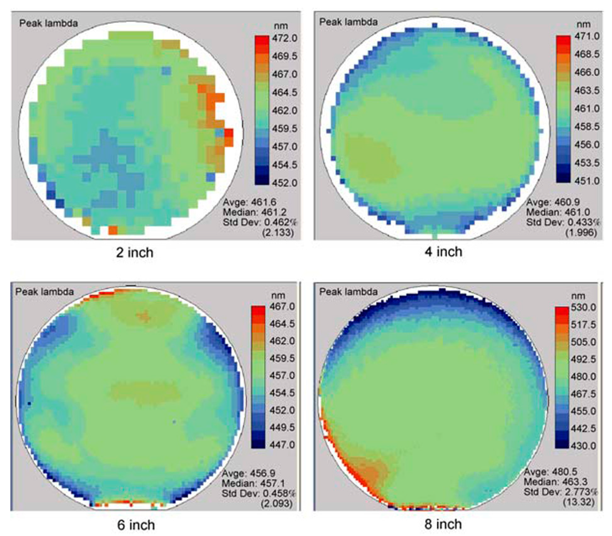
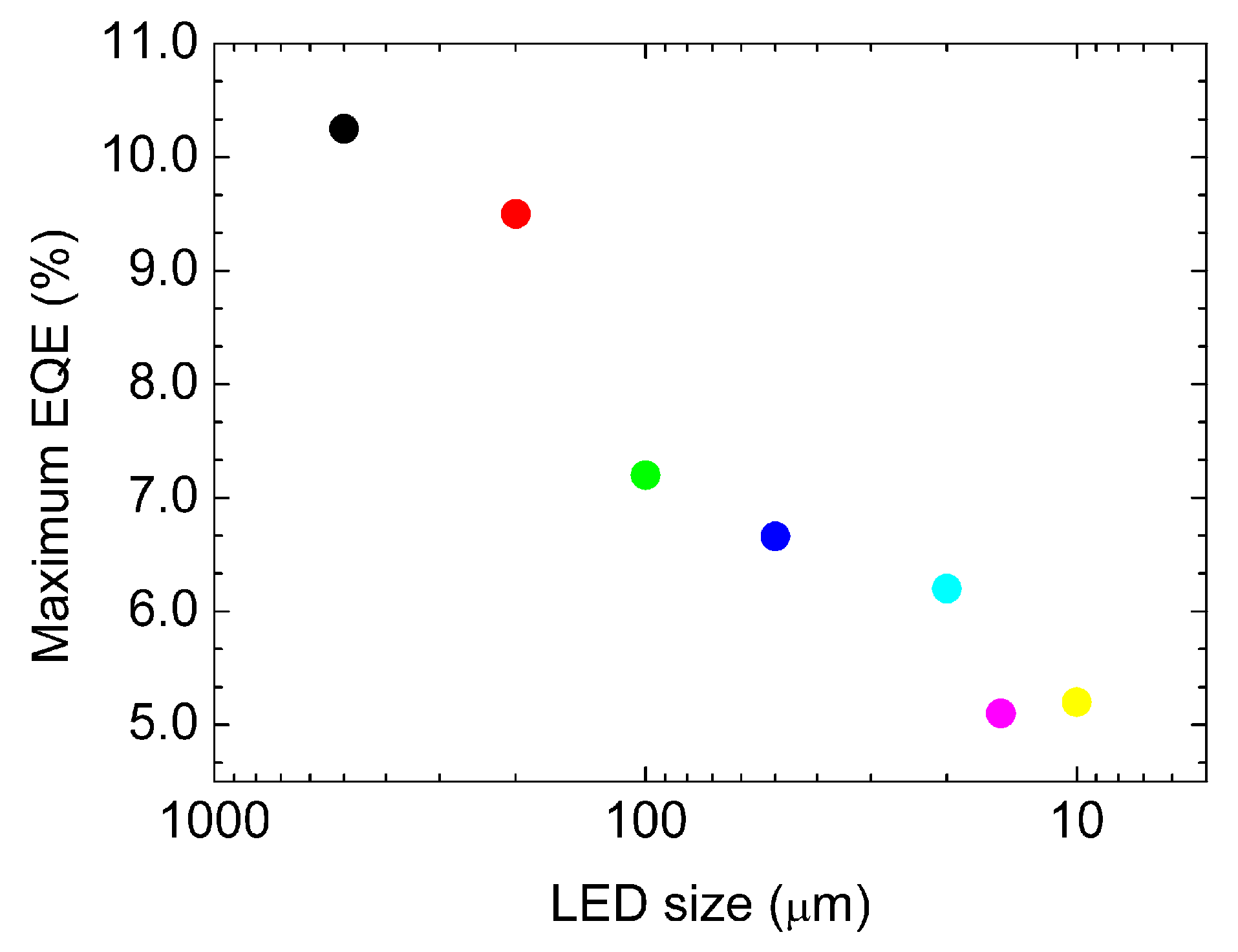
2. Epitaxy and Chip Processing
3. Assembly Technologies
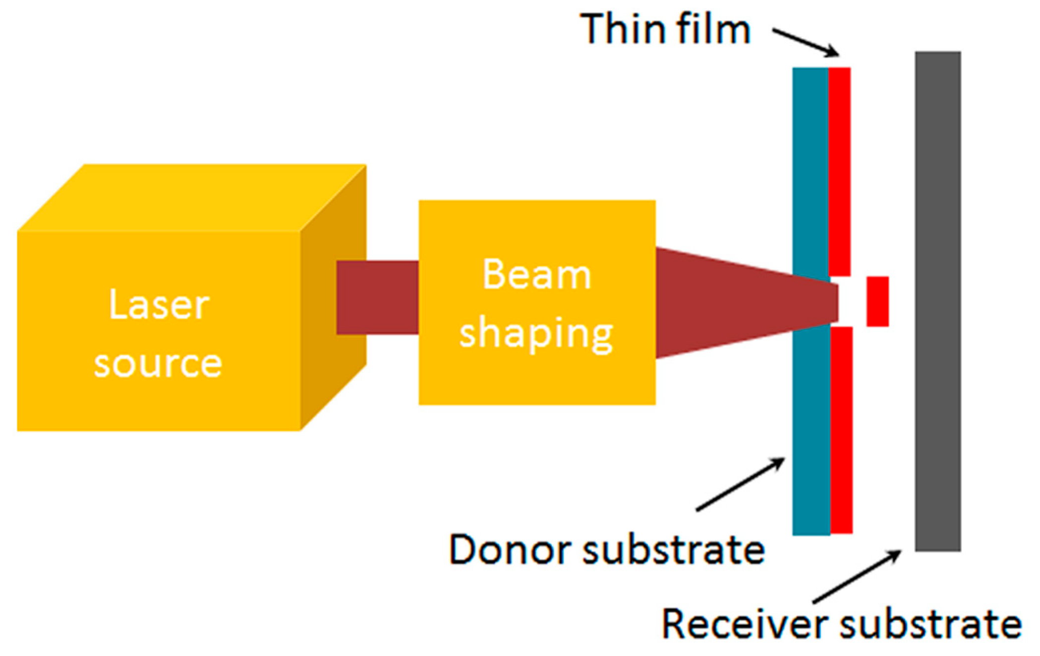
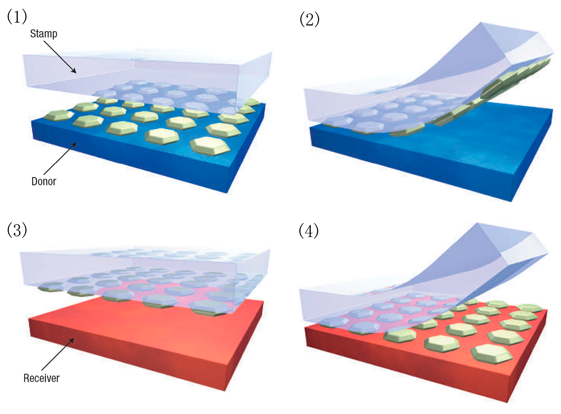
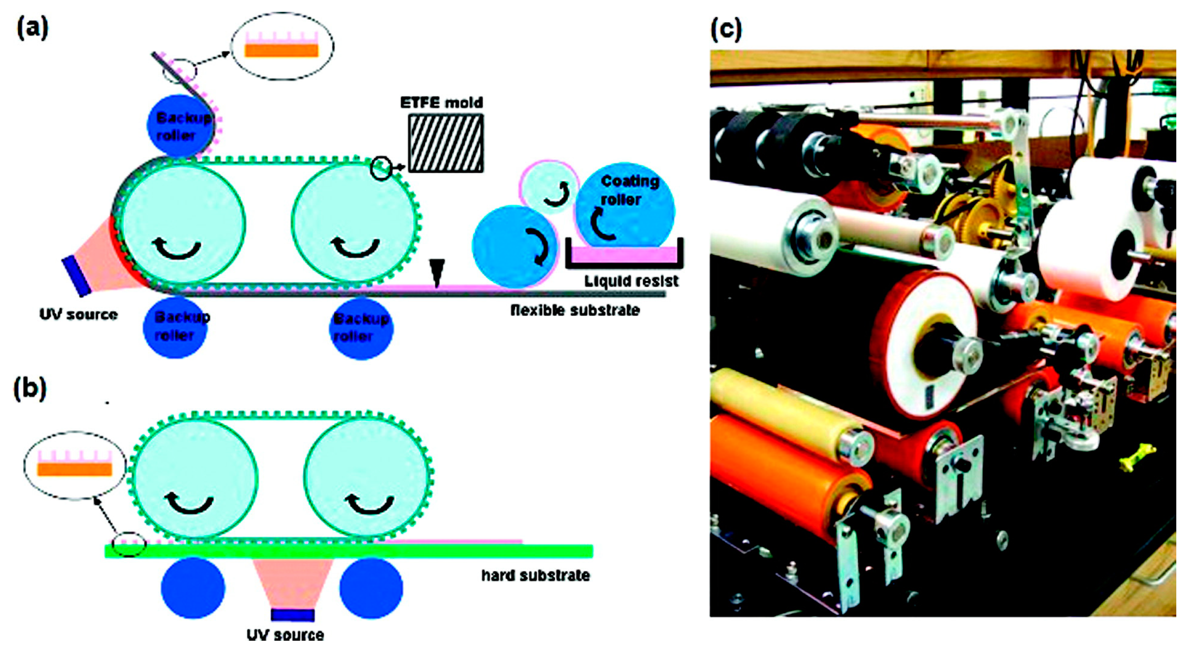
3.1. Mass Transfer Technologies
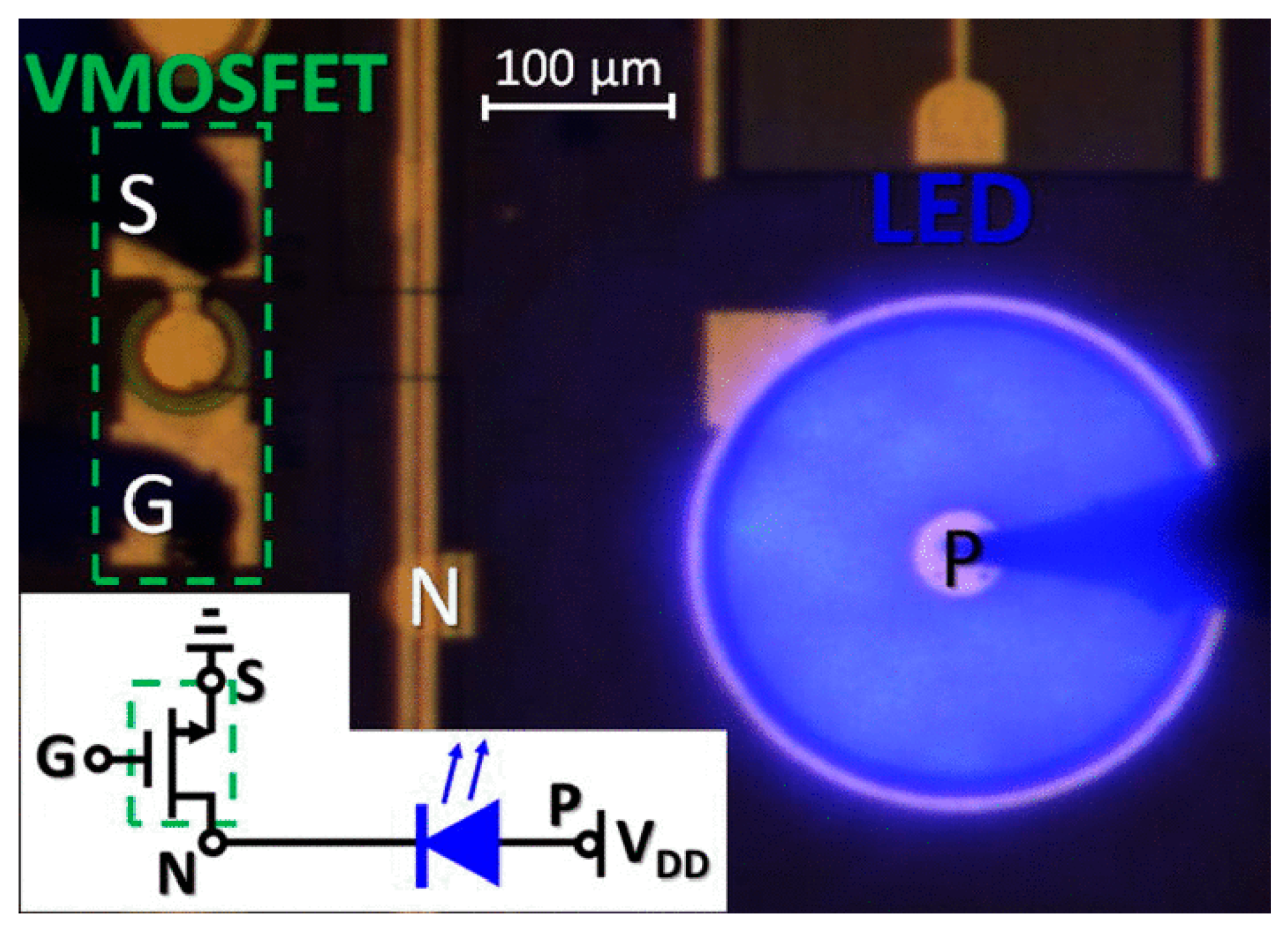
3.2. Monolithic Fabrication of Micro-Displays
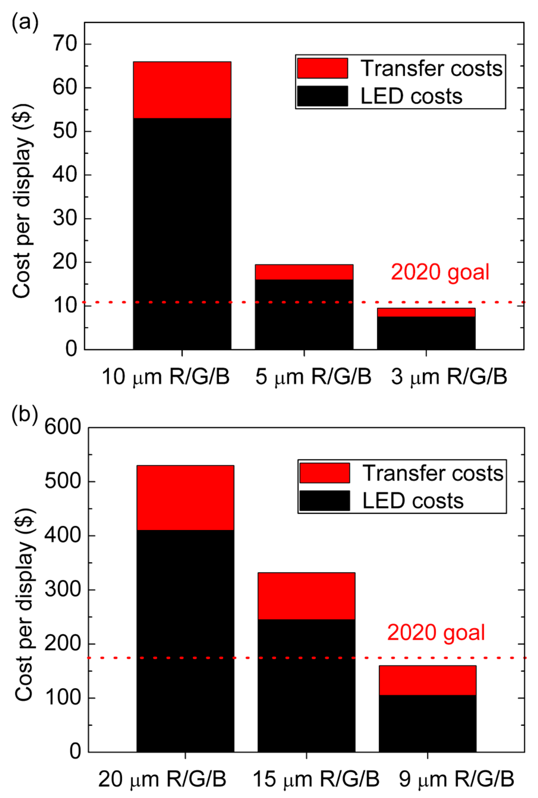
4. Full-Color Schemes
5. Current Challenges and Prospects
Author Contributions
Conflicts of Interest
References
- Jiang, H.X.; Lin, J.Y. Nitride micro-LEDs and beyond—A decade progress review. Opt. Express 2013, 21, A475. [Google Scholar] [CrossRef] [PubMed]
- Fan, J.Y.; Lin, J.Y.; Jiang, H.X. III-nitride micro-emitter arrays: Development and applications. J. Phys. D Appl. Phys. 2008, 41, 094001. [Google Scholar] [CrossRef]
- Dupré, L.; Marra, M.; Verney, V.; Aventurier, B.; Henry, F.; Olivier, F.; Tirano, S.; Daami, A.; Templier, F. Processing and characterization of high resolution GaN/InGaN LED arrays at 10 micron pitch for micro display applications. In Proceedings of the SPIE, Warsaw, Poland, 4–8 July 2017; Volume 10104. [Google Scholar]
- Radauscher, E.J.; Meitl, M.; Prevatte, C.; Bonafede, S.; Rotzoll, R.; Gomez, D.; Moore, T.; Raymond, B.; Cok, R.; Fecioru, A. Miniaturized LEDs for flat-panel displays. In Proceedings of the SPIE, San Francisco, CA, USA, 30 January–1 February 2017; Volume 10124, p. 1012418. [Google Scholar]
- Olivier, F.; Daami, A.; Dupré, L.; Henry, F.; Aventurier, B.; Templier, F. 25-4: Investigation and improvement of 10 μm Pixelpitch GaN-based Micro-LED arrays with very high brightness. SID Int. Symp. Dig. Tech. Pap. 2017, 48, 353. [Google Scholar] [CrossRef]
- Poher, V.; Grossman, N.; Kennedy, G.T.; Nikolic, K.; Zhang, H.X.; Gong, Z.; Drakakis, E.M.; Gu, E.; Dawson, M.D.; French, P.M.W. Micro-LED arrays: A tool for two-dimensional neuron stimulation. J. Phys. D Appl. Phys. 2008, 41, 094014. [Google Scholar] [CrossRef]
- Grossman, N.; Poher, V.; Grubb, M.S.; Kennedy, G.T.; Nikolic, K.; McGovern, B.; Berlinguer Palmini, R.; Gong, Z.; Drakakis, E.M.; Neil, M.A.; et al. Multi-site optical excitation using ChR2 and micro-LED array. J. Neural Eng. 2010, 7, 016004. [Google Scholar] [CrossRef]
- Zarowna-Dabrowska, A.; Neale, S.L.; Massoubre, D.; McKendry, J.; Rae, B.R.; Henderson, R.K.; Rose, M.J.; Yin, H.; Cooper, J.M.; Gu, E. Miniaturized optoelectronic tweezers controlled by GaN micro-pixel light emitting diode arrays. Opt. Express 2011, 19, 2720. [Google Scholar] [CrossRef]
- Goßler, C.; Bierbrauer, C.; Moser, R.; Kunzer, M.; Holc, K.; Pletschen, W.; Köhler, K.; Wagner, J.; Schwaerzle, M.; Ruther, P. GaN-based micro-LED arrays on flexible substrates for optical cochlear implants. J. Phys. D Appl. Phys. 2014, 47, 205401. [Google Scholar] [CrossRef]
- Guilhabert, B.; Massoubre, D.; Richardson, E.; McKendry, J.J.D.; Valentine, G.; Henderson, R.K.; Watson, I.M.; Gu, E.; Dawson, M.D. Sub-micron lithography using InGaN micro-LEDs: mask-free fabrication of LED arrays. IEEE Photonics Technol. Lett. 2012, 24, 2221–2224. [Google Scholar] [CrossRef]
- Zhao, L.; Zhu, S.; Wu, C.; Yang, C.; Yu, Z.; Yang, H.; Liu, L. GaN-based LEDs for light communication. Sci. China Phys. Mech. Astron. 2016, 59, 107301. [Google Scholar] [CrossRef]
- Chun, H.; Rajbhandari, S.; Faulkner, G.; Tsonev, D.; Xie, E.; James, J.; McKendry, D.; Gu, E.; Dawson, M.D.; O’Brien, D.C.; et al. LED based wavelength division multiplexed 10 Gb/s visible light communications. Lightwave Technol. 2016, 34, 3047–3052. [Google Scholar] [CrossRef]
- McKendry, J.J.D.; Green, R.P.; Kelly, A.E.; Gong, Z.; Guilhabert, B.; Massoubre, D.; Gu, E.; Dawson, M.D. High-speed visible light communications using individual pixels in a micro light-emitting diode array. IEEE Photonics Technol. Lett. 2010, 22, 1346–1348. [Google Scholar] [CrossRef]
- Rajbhandari, S.; McKendry, J.J.D.; Herrnsdorf, J.; Chun, H.; Faulkner, G.; Haas, H.; Watson, I.M.; O’Brien, D.; Dawson, M.D. A review of gallium nitride LEDs for multi-gigabit-per-second visible light data communications. Semicon. Sci. Technol. 2017, 32, 023001. [Google Scholar] [CrossRef]
- Konoplev, S.S.; Bulashevich, K.A.; Karpov, S.Y. From Large-Size to Micro-LEDs: Scaling Trends Revealed by Modeling. Phys. Stat. Sol. A 2018, 215, 1700508. [Google Scholar] [CrossRef]
- Choi, H.W.; Jeon, C.W.; Dawson, M.D.; Edwards, P.R.; Martin, R.W.; Tripathy, S. Mechanism of enhanced light output efficiency in InGaN-based microlight emitting diodes. J. Appl. Phys. 2003, 93, 5978–5982. [Google Scholar] [CrossRef]
- Thibeault, B.; DenBaars, S. Enhanced light extraction through the use of micro-LED arrays. Patent No. 6,410,942, 25 June 2002. [Google Scholar]
- Adivarahan, V.; Wu, S.; Sun, W.H.; Mandavilli, V.; Shatalov, M.S.; Simin, G.; Yang, J.W.; Maruska, H.P.; Asif Khan, M. High-power deep ultraviolet light-emitting diodes basedon a micro-pixel design. Appl. Phys. Lett. 2004, 85, 1838–1840. [Google Scholar] [CrossRef]
- Virey, E.H.; Baron, N. Status and Prospects of microLED Displays. SID Int. Symp. Dig. Tech. Pap. 2018, 49, 593–596. [Google Scholar] [CrossRef]
- Beckers, A.; Fahle, D.; Mauder, C.; Kruecken, T.; Boyd, A.R.; Heuken, M. Enabling the Next Era of Display Technologies by Micro LED MOCVD Processing. SID Int. Symp. Dig. Tech. Pap. 2018, 49, 601–603. [Google Scholar] [CrossRef]
- Paranjpe, A.; Montgomery, J.; Lee, S.M.; Morath, C. Micro-LED Displays: Key Manufacturing Challenges and Solutions. SID Int. Symp. Dig. Tech. Pap. 2018, 49, 597–600. [Google Scholar] [CrossRef]
- Amour, E.; Lu, F.; Belousov, M.; Lee, D.; Quinn, W. LED growth compatibility between 2”, 4” and 6” sapphire. Semicond. Today 2009, 4, 82–86. [Google Scholar]
- Lu, F.; Lee, D.; Byrnes, D.; Armour, E.; Quinn, W. Blue LED growth from 2 inch to 8 inch. Sci. China Technol. Sci. 2011, 54, 33–37. [Google Scholar] [CrossRef]
- Aida, H.; Lee, D.S.; Belousov, M.; Sunakawa, K. Effect of Initial Bow of Sapphire Substrate on Substrate Curvature during InGaN Growth Stage of Light Emitting Diode Epitaxy. Jpn. J. Appl. Phys. 2012, 51, 012102. [Google Scholar] [CrossRef]
- Aida, H.; Aota, N.; Takeda, H.; Koyama, K. Control of initial bow of sapphire substrates for III-nitride epitaxy by internally focused laser processing. J. Cryst. Growth 2012, 361, 135–141. [Google Scholar] [CrossRef]
- Hoffmann, V.; Knauer, A.; Brunner, C.; Einfeldt, S.; Weyers, M.; Tränkle, G.; Haberland, K.; Zettler, J.T.; Kneissl, M. Uniformity of the wafer surface temperature during MOVPE growth of GaN-based laser diode structures on GaN and sapphire substrate. J. Cryst. Growth 2011, 315, 5–9. [Google Scholar] [CrossRef]
- Aida, H.; Takeda, H.; Aota, N.; Koyama, K. Reduction of bowing in GaN-on-sapphire and GaN-on-silicon substrates by stress implantation by internally focused laser processing. Jpn. J. Appl. Phys. 2011, 51, 016504. [Google Scholar] [CrossRef]
- Liu, Z.J.; Chong, W.C.; Wong, K.M.; Keung, C.W.; Lau, K.M. Investigation of Forward Voltage Uniformity in Monolithic Light-Emitting Diode Arrays. IEEE Photonics Technol. Lett. 2013, 25, 1290–1293. [Google Scholar] [CrossRef]
- Xie, E.; Stonehouse, M.; Ferreira, R.; Jonathan, J.; McKendry, D.; Herrnsdorf, J.; He, X.; Rajbhandari, S.; Chun, H.; Aravind, V.; et al. Design, Fabrication, and Application of GaN-Based Micro-LED Arrays With Individual Addressing by N-Electrodes. IEEE Photonics J. 2017, 9, 7907811. [Google Scholar] [CrossRef]
- Hwang, D.; Mughal, A.; Pynn, C.D.; Nakamura, S.; DenBaars, S.P. Sustained high external quantum efficiency in ultrasmall blue III–nitride micro-LEDs. Appl. Phys. Express 2017, 10, 032101. [Google Scholar] [CrossRef]
- Olivier, F.; Tirano, S.; Dupré, L.; Aventurier, B.; Largeron, C.; Templier, F. Influence of size-reduction on the performances of GaN-based micro-LEDs for display application. J. Lumin. 2017, 191, 112–116. [Google Scholar] [CrossRef]
- Chen, W.; Hu, G.; Lin, J.; Jiang, J.; Liu, M.; Yang, Y.; Hu, G.; Lin, Z.; Wu, Z.; Liu, Y. High-performance, single-pyramid micro light-emitting diode with leakage current confinement layer. Appl. Phys. Express 2015, 8, 032102. [Google Scholar] [CrossRef]
- Wong, M.S.; Hwang, D.; Alhassan, A.I.; Lee, C.; Ley, R.; Nakamura, S.; DenBaars, S.P. High efficiency of III-nitride micro-light-emitting diodes by sidewall passivation using atomic layer deposition. Opt. Express 2018, 26, 21324–21331. [Google Scholar] [CrossRef]
- Lee, V.W.; Twu, N.; Kymissis, I. Frontline technology micro-LED technologies and applications. Inf. Disp. 2016, 32, 16–23. [Google Scholar]
- Delaporte, P.; Alloncle, A.-P. Laser-induced forward transfer: A high resolution additive manufacturing technology. Opt. Laser Technol. 2016, 78, 33–41. [Google Scholar] [CrossRef]
- Marinov, V.R. Laser-Enabled Extremely-High Rate Technology for µLED Assembly. SID Int. Symp. Dig. Tech. Pap. 2018, 49, 692–695. [Google Scholar] [CrossRef]
- Yeh, H.-J.J.; Smith, J.S. Fluidic self-assembly for the integration of GaAs light-emitting diodes on Si substrates. IEEE Photonics Technol. Lett. 1994, 6, 706–708. [Google Scholar] [CrossRef]
- Saeedi, E.; Kim, S.S.; Parviz, B.A. Self-assembled inorganic micro-display on plastic. In Proceedings of the 2007 IEEE 20th International Conference on Micro Electro Mechanical Systems (MEMS), Hyogo, Japan, 21–25 January 2007. [Google Scholar]
- Schuele, P.J.; Sasaki, K.; Ulmer, K.; Lee, J.-J. Display with surface mount emissive elements. Patent No. 9,825,202, 11 May 2017. [Google Scholar]
- Bibl, A.; Higginson, J.A.; Hu, H.-H.; Law, H.-F.S. Method of transferring and bonding an array of micro devices. Patent No. 9,773,750, 26 September 2017. [Google Scholar]
- Meitl, M.A.; Zhu, Z.-T.; Kumar, V.; Lee, K.J.; Feng, X.; Huang, Y.Y.; Adesida, I.; Nuzzo, R.G.; Rogers, J.A. Transfer printing by kinetic control of adhesion to an elastomeric stamp. Nat. Mater. 2006, 5, 33. [Google Scholar] [CrossRef]
- Ahn, S.H.; Guo, L.J. Large-area roll-to-roll and roll-to-plate nanoimprint lithography: a step toward high-throughput application of continuous nanoimprinting. ACS Nano 2009, 3, 2304–2310. [Google Scholar] [CrossRef]
- Sharma, B.K.; Jang, B.; Lee, J.E.; Bae, S.-H.; Kim, T.W.; Lee, H.-J.; Kim, J.-H.; Ahn, J.-H. Load-Controlled Roll Transfer of Oxide Transistors for Stretchable Electronics. Adv. Funct. Mater. 2013, 23, 2024–2032. [Google Scholar] [CrossRef]
- Liu, Z.J.; Huang, T.; Ma, J.; Liu, C.; Lau, K.M. Monolithic integration of AlGaN/GaN HEMT on LED by MOCVD. IEEE Electron. Dev. Lett. 2014, 35, 330–332. [Google Scholar] [CrossRef]
- Lu, X.; Liu, C.; Jiang, H.; Zou, X.; Zhang, A.; Lau, K.M. Monolithic integration of enhancement-mode vertical driving transistorson a standard InGaN/GaN light emitting diode structure. Appl. Phys. Lett. 2016, 109, 053504. [Google Scholar] [CrossRef]
- Liu, C.; Cai, Y.; Zou, X.; Lau, K.M. Low-leakage high-breakdown laterally integrated HEMT-LED via n-GaN electrode. IEEE Photonics Technol. Lett. 2016, 28, 1130–1133. [Google Scholar] [CrossRef]
- Lee, Y.-J.; Yang, Z.-P.; Chen, P.-G.; Hsieh, Y.-A.; Yao, Y.-C.; Liao, M.-H.; Lee, M.-H.; Wang, M.-T.; Hwang, J.-M. Monolithic integration of GaN-based light-emitting diodes and metal-oxide-semiconductor field-effect transistors. Opt. Express 2014, 22, A1589–A1595. [Google Scholar] [CrossRef]
- Tsuchiyama, K.; Yamane, K.; Sekiguchi, H.; Okada, H.; Wakahara, A. Fabrication of Si/SiO2/GaN structure by surface-activated bonding for monolithic integration of optoelectronic devices. Jpn. J. Appl. Phys. 2016, 55, 05FL01. [Google Scholar] [CrossRef]
- Tsuchiyama, K.; Yamane, K.; Utsunomiya, S.; Sekiguchi, H.; Okada, H.; Wakahara, A. Monolithic integration of Si-MOSFET and GaN-LED using Si/SiO2/GaN-LED wafer. Appl. Phys. Express 2016, 9, 104101. [Google Scholar] [CrossRef]
- Lau, K.M.; Keung, C.W.; Liu, Z. Method for manufacturing a monolithic LED micro-display on an active matrix panel using flip-chip technology and display apparatus having the monolithic LED micro-display. Patent No. 8,557,616, 15 October 2013. [Google Scholar]
- Day, J.; Li, J.; Lie, D.Y.C.; Bradford, C.; Lin, J.Y.; Jiang, H.X. III-Nitride full-scale high-resolution microdisplays. Appl. Phys. Lett. 2011, 99, 031116. [Google Scholar] [CrossRef]
- Marion, F.; Bisotto, S.; Berger, F.; Gueugnot, A.; Mathieu, L.; Henry, D.; Templier, F.; Catelain, T. A room temperature flip-chip technology for high pixel count micro-displays and imaging arrays. In Proceedings of the IEEE 66th Electronic Components and Technology Conference (ECTC), Las Vegas, NV, USA, 31 May–3 June 2016. [Google Scholar]
- Templier, F.; Dupré, L.; Dupont, B.; Daami, A.; Aventurier, B.; Henry, F.; Sarrasin, D.; Renet, S.; Berger, F.; Olivier, F. High-resolution active-matrix 10-μm pixel-pitch GaN LED microdisplays for augmented reality applications. In Proceedings of the SPIE 10556, Strasbourg, France, 22–26 April 2018; p. 105560I. [Google Scholar]
- Even, A.; Laval, G.; Ledoux, O.; Ferret, P.; Sotta, D.; Guiot, E.; Levy, F.; Robin, I.C.; Dussaigne, A. Enhanced In incorporation in full InGaN heterostructure grown on relaxed InGaN pseudo-substrate. Appl. Phys. Lett. 2017, 110, 262103. [Google Scholar] [CrossRef]
- Even, A. In incorporation Improvement in InGaN Based Active Region Using InGaN Pseudo Substrate for Monolithic White LED Application; Université Grenoble Alpes: Saint-Martin-d’Hères, France, 2018. [Google Scholar]
- Han, H.-W.; Lin, H.-Y.; Lin, C.-C.; Chong, W.-C.; Li, J.-R.; Chen, K.-J.; Yu, P.; Chen, T.-M.; Chen, H.-M.; Lau, K.-M. Resonant-enhanced full-color emission of quantum-dot-based micro LED display technology. Opt. Express 2015, 23, 32504–32515. [Google Scholar] [CrossRef]
- Rudorfer, A.; Tscherner, M.; Palfinger, C.; Reil, F.; Hartmann, P.; Seferis, I.E.; Zych, E.; Wenzl, F.P. A study on Aerosol jet printing technology in LED module manufacturing. In Proceedings of the SPIE 9954, San Diego, CA, USA, 7 September 2016; p. 99540E. [Google Scholar]
- Singh, M.; Haverinen, H.M.; Dhagat, P.; Jabbour, G.E. Inkjet printing-process and its applications. Adv. Mater. 2010, 22, 673–685. [Google Scholar] [CrossRef]
- Chen, K.-J.; Chen, H.-C.; Tsai, K.-A.; Lin, C.-C.; Tsai, H.-H.; Chien, S.-H.; Cheng, B.-S.; Hsu, Y.-J.; Shih, M.-H.; Tsai, C.-H. Resonant-enhanced full-color emission of quantum-dot-based display technology using a pulsed spray method. Adv. Funct. Mater. 2012, 22, 5138–5143. [Google Scholar] [CrossRef]
- Han, J.K.; Choi, J.I.; Piquette, A.; Hannah, M.; Anc, M.; Galvez, M.; Talbot, J.B.; McKittrick, J. Phosphor development and integration for near-UV LED solid state lighting. ECS J. Solid State Sci. Technol. 2013, 2, R3138. [Google Scholar] [CrossRef]
- Chen, D.-C.; Liu, Z.-G.; Deng, Z.-H.; Wang, C.; Cao, J.-G.; Liu, Q.-L. Optimization of light efficacy and angular color uniformity by hybrid phosphor particle size for white light-emitting diode. Rare Met. 2014, 33, 348–352. [Google Scholar] [CrossRef]
- Xie, B.; Hu, R.; Luo, X.J. Quantum dots-converted light-emitting diodes packaging for lighting and display: status and perspectives. Electron. Packag. 2016, 138, 020803. [Google Scholar] [CrossRef]
- McKittrick, J.; Shea-Rohwer, L.E. Down conversion materials for solid-state lighting. J. Am. Ceram. Soc. 2014, 97, 1327–1352. [Google Scholar] [CrossRef]
- Lin, H.-Y.; Sher, C.-W.; Hsieh, D.-H.; Chen, X.-J.; Chen, H.-M.P.; Chen, T.-M.; Lau, K.-M.; Chen, C.-H.; Lin, C.-C.; Kuo, H.-C. Optical cross-talk reduction in a quantum-dot-based full-color micro-light-emitting-diode display by a lithographic-fabricated photoresist mold. Photonics Res. 2017, 5, 411–416. [Google Scholar] [CrossRef]
- Chen, G.-S.; Wei, B.-Y.; Lee, C.-T.; Lee, H.Y. Monolithic red/green/blue micro-LEDs with HBR and DBR structures. IEEE Photonics Technol. Lett. 2018, 30, 262–265. [Google Scholar] [CrossRef]
- Gou, F.; Hsiang, E.-L.; Tan, G.; Lan, Y.-F.; Tsai, C.-Y.; Wu, S.-T. Tripling the Optical Efficiency of Color-Converted Micro-LED Displays with Funnel-Tube Array. Crystals 2019, 9, 39. [Google Scholar] [CrossRef]
- An, C.-C.; Wu, M.-H.; Huang, Y.-W.; Chen, T.-H.; Chao, C.-H.; Yeh, W.-Y. Study on flip chip assembly of high density micro-LED array. In Proceedings of the 6th International Microsystems, Packaging, Assembly and Circuits Technology Conference (IMPACT), Taipei, Taiwan, 19–21 October 2011; pp. 336–338. [Google Scholar]
- Henry, W.; Percival, C. ILED Displays: Next Generation Display Technology. SID Int. Symp. Dig. Tech. Pap. 2016, 47, 747–750. [Google Scholar] [CrossRef]
- Chaji, R.; Fathi, E.; Zamani, A. Low-Cost Micro-LED Displays for All Applications. SID Int. Symp. Dig. Tech. Pap. 2017, 48, 264–267. [Google Scholar] [CrossRef]


| Methods | Company/Institute | Force/means | Transfer rate |
|---|---|---|---|
| Laser lift-off | Optovate/Uniqarta | Laser | 1000 per shot/100 million per hour |
| Fluidic assembly | Foxconn(eLux) | Gravity and capillary | 50 million per hour |
| Electrostatic array | Apple (LuxVue) | Electrostatic | (Not found) |
| elastomer stamp | X-Celeprint | van der Waals | 1 million per hour |
| Roll-to-roll | KIMM | Roll stamp | 10,000 per sec |
© 2019 by the authors. Licensee MDPI, Basel, Switzerland. This article is an open access article distributed under the terms and conditions of the Creative Commons Attribution (CC BY) license (http://creativecommons.org/licenses/by/4.0/).
Share and Cite
Ding, K.; Avrutin, V.; Izyumskaya, N.; Özgür, Ü.; Morkoç, H. Micro-LEDs, a Manufacturability Perspective. Appl. Sci. 2019, 9, 1206. https://doi.org/10.3390/app9061206
Ding K, Avrutin V, Izyumskaya N, Özgür Ü, Morkoç H. Micro-LEDs, a Manufacturability Perspective. Applied Sciences. 2019; 9(6):1206. https://doi.org/10.3390/app9061206
Chicago/Turabian StyleDing, Kai, Vitaliy Avrutin, Natalia Izyumskaya, Ümit Özgür, and Hadis Morkoç. 2019. "Micro-LEDs, a Manufacturability Perspective" Applied Sciences 9, no. 6: 1206. https://doi.org/10.3390/app9061206
APA StyleDing, K., Avrutin, V., Izyumskaya, N., Özgür, Ü., & Morkoç, H. (2019). Micro-LEDs, a Manufacturability Perspective. Applied Sciences, 9(6), 1206. https://doi.org/10.3390/app9061206