Low-Damage Reactive Ion Etching of Nanoplasmonic Waveguides with Ultrathin Noble Metal Films


Abstract
1. Introduction
2. Materials and Methods
3. Results and Discussion
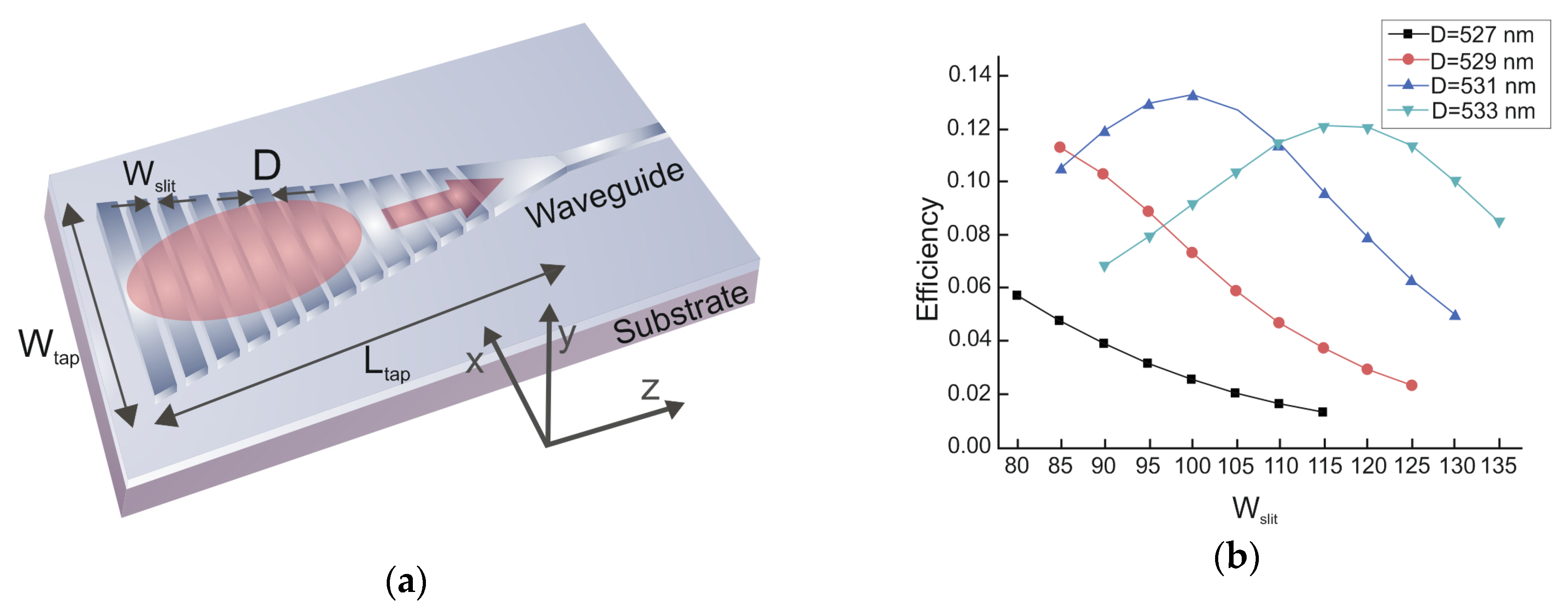
3.1. Long-Range Dielectric-Loaded Surface Plasmon-Polariton Waveguides (LR-DLSPPW) Simulation and Analysis
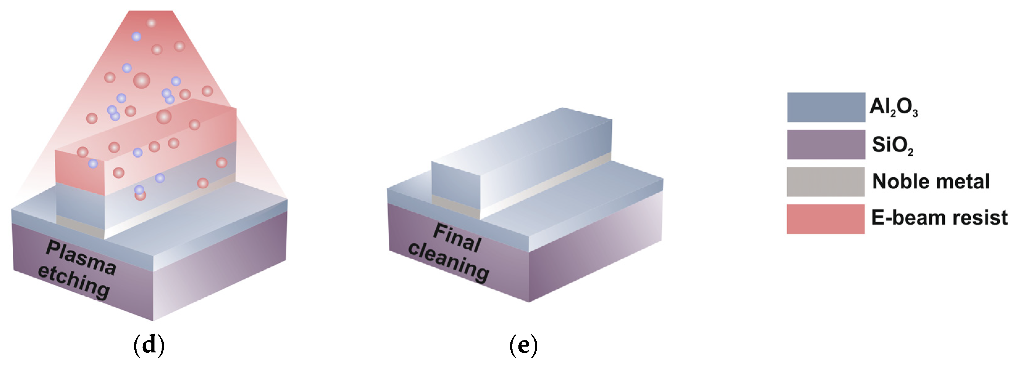
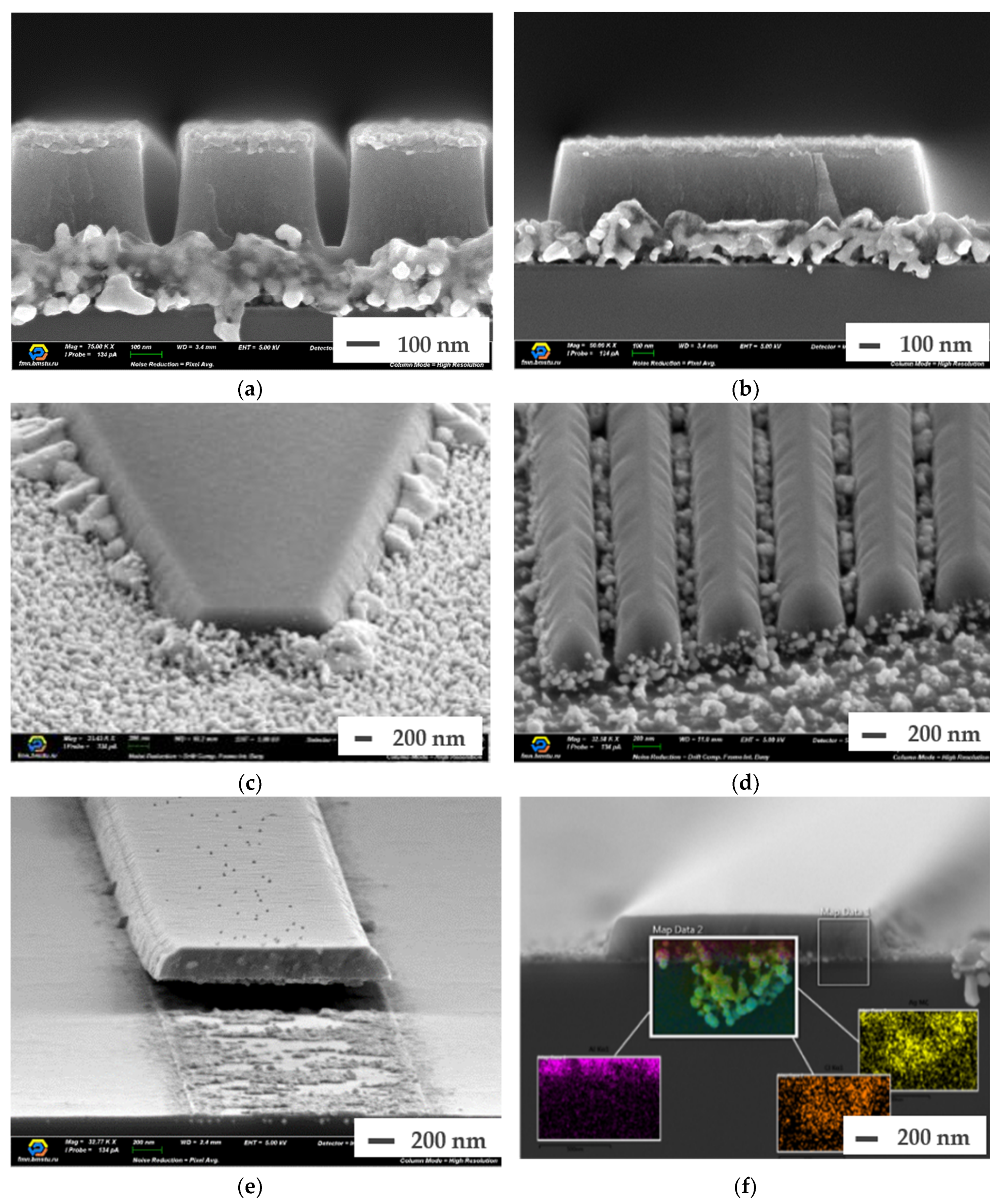
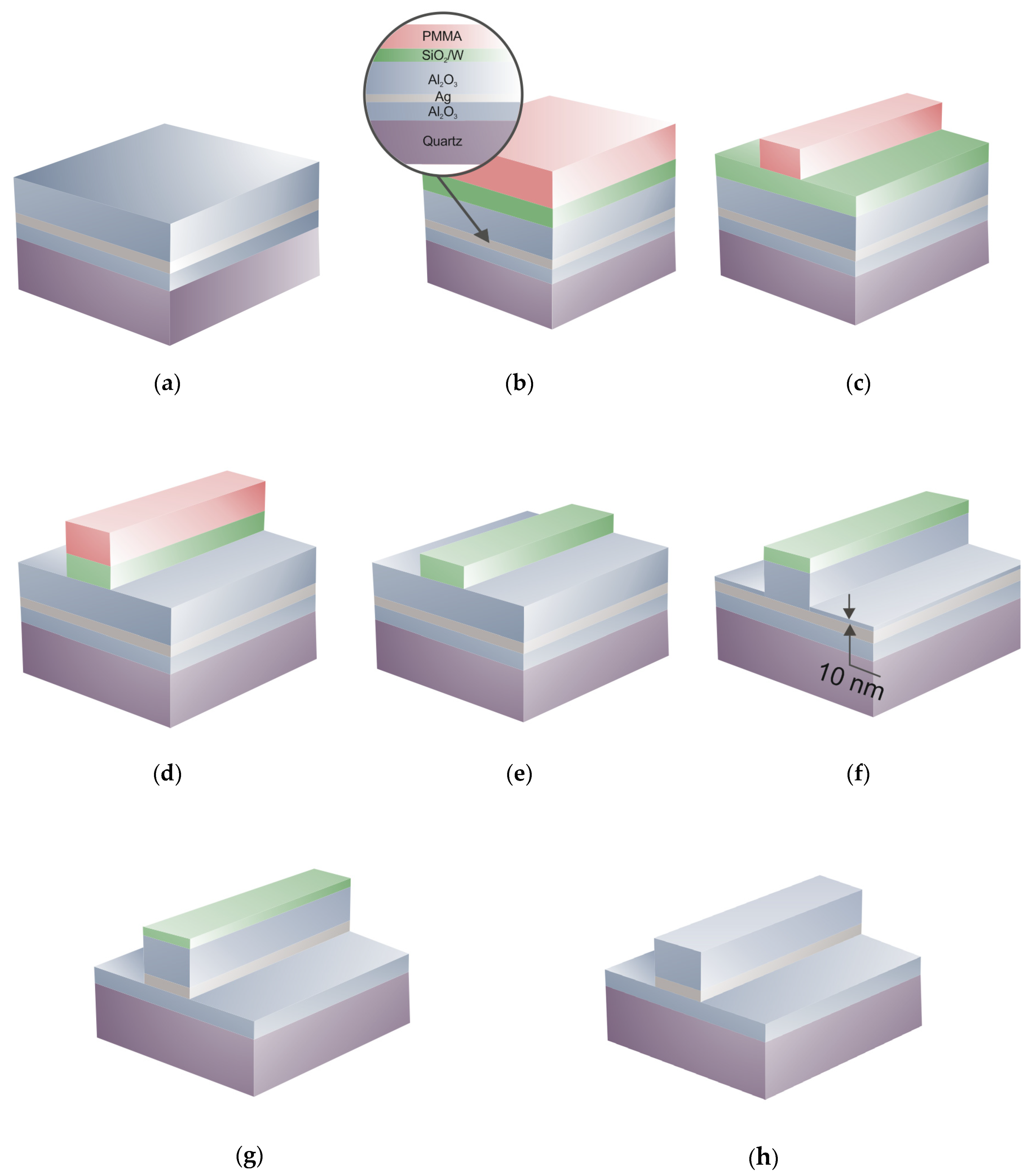
3.2. LR-DLSPPW Fabrication Process Flow and Key Issues
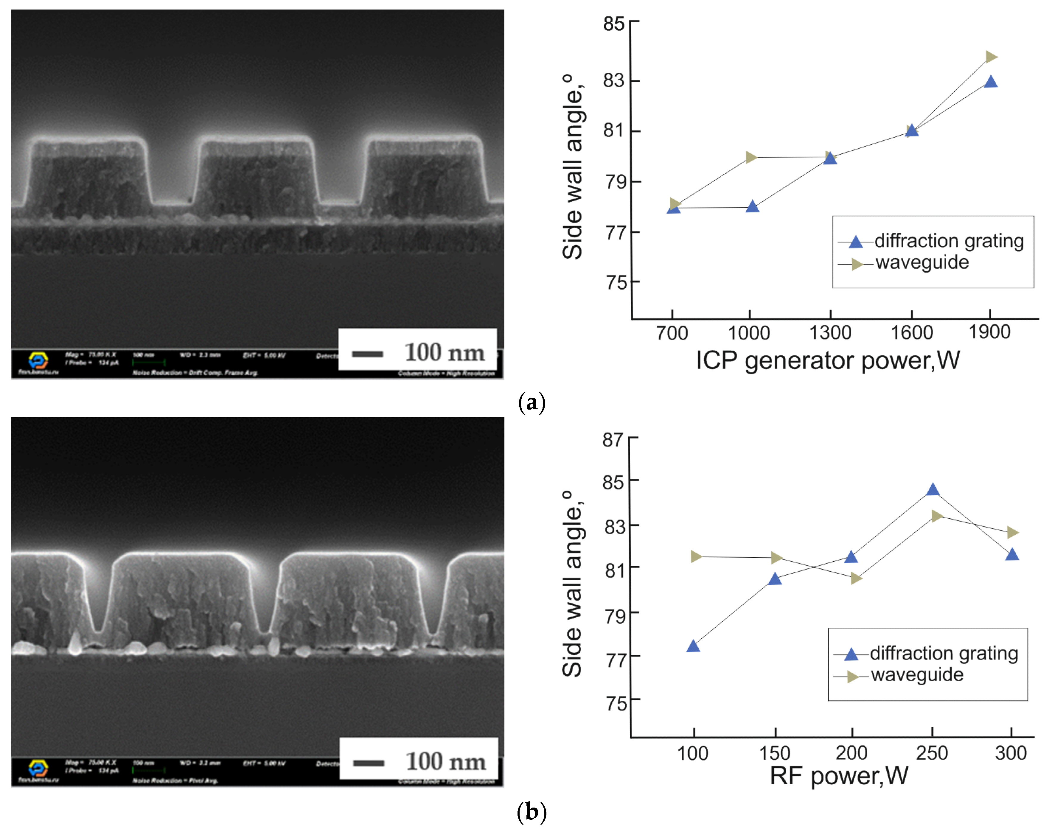
3.3. Al2O3/Ag (Au)/Al2O3 Dry Etching Process
4. Conclusions
Author Contributions
Funding
Acknowledgments
Conflicts of Interest
References
- Miller, D.A.B. Optical interconnects to electronic chips. Appl. Opt. 2010, 49, F59–F70. [Google Scholar] [CrossRef] [PubMed]
- Atabaki, A.H.; Moazeni, S.; Pavanello, F.; Gevorgyan, H.; Notaros, J.; Alloatti, L.; Wade, M.T.; Sun, C.; Kruger, S.A.; Meng, H.; et al. Integrating photonics with silicon nanoelectronics for the next generation of systems on a chip. Nature 2018, 556, 349–354. [Google Scholar] [CrossRef] [PubMed]
- Kim, J.T.; Ju, J.J.; Park, S.; Kim, M.-S.; Park, S.K.; Lee, M.-H. Chip-to-chip optical interconnect using gold long-range surface plasmon polariton waveguides. Opt. Express 2008, 16, 13133–13138. [Google Scholar] [CrossRef] [PubMed]
- Nelson, B.; Keeler, G.; Agarwal, D.; Helman, N.; Miller, D. Wavelength division multiplexed optical interconnect using short pulses. IEEE J. Sel. Top. Quantum Electron. 2003, 9, 486–491. [Google Scholar] [CrossRef]
- Sun, C.; Georgas, M.; Orcutt, J.; Moss, B.; Chen, Y.-H.; Shainline, J.; Wade, M.; Mehta, K.; Nammari, K.; Timurdogan, E.; et al. A monolithically-integrated chip-to-chip optical link in bulk CMOS. IEEE J. Solid-State Circuits 2015, 50, 828–844. [Google Scholar] [CrossRef]
- Sun, C.; Wade, M.T.; Lee, Y.; Orcutt, J.S.; Alloatti, L.; Georgas, M.S.; Waterman, A.S.; Shainline, J.M.; Avizienis, R.R.; Lin, S.; et al. Single-chip microprocessor that communicates directly using light. Nature 2015, 528, 534–538. [Google Scholar] [CrossRef]
- NAVOLCHI Project. Available online: https://www.imt.kit.edu/projects/navolchi/ (accessed on 25 September 2019).
- Melikyan, A.; Alloatti, L.; Muslija, A.; Hillerkuss, D.; Schindler, P.C.; Li, J.; Palmer, R.; Korn, D.; Muehlbrandt, S.; Van Thourhout, D.; et al. High-speed plasmonic phase modulators. Nat. Photonics 2014, 8, 229–233. [Google Scholar] [CrossRef]
- Melikyan, A.; Koehnle, K.; Lauermann, M.; Palmer, R.; Koeber, S.; Muehlbrandt, S.; Schindler, P.C.; Elder, D.L.; Wolf, S.; Heni, W.; et al. Plasmonic-organic hybrid (POH) modulators for OOK and BPSK signaling at 40 Gbit/s. Opt. Express 2015, 23, 9938–9946. [Google Scholar] [CrossRef]
- Dolores-Calzadilla, V.; Fiore, A.; Smit, M.K. Towards Plasmonic Lasers for Optical Interconnects. In Proceedings of the 14th International Conference on Transparent Optical Networks (ICTON), Coventry, UK, 2–5 July 2012; pp. 1–4. [Google Scholar]
- Baburin, A.S.; Ivanov, A.I.; Trofimov, I.V.; Dobronosovaa, A.A.; Melentiev, P.N.; Balykin, V.I.; Rodionov, I.A. Highly directional plasmonic nanolaser based on high-performance noble metal film photonic crystal. In Proc. SPIE 10672, Nanophotonics VII; International Society for Optics and Photonics: Bellingham, WA, USA, 2018. [Google Scholar] [CrossRef]
- Melentiev, P.; Kalmykov, A.; Gritchenko, A.; Afanasiev, A.; Balykin, V.; Baburin, A.S.; Ryzhova, E.; Filippov, I.; Rodionov, I.A.; Nechepurenko, I.A.; et al. Plasmonic nanolaser for intracavity spectroscopy and sensorics. Appl. Phys. Lett. 2017, 111, 213104. [Google Scholar] [CrossRef]
- Lott, J.A.; Payusov, A.S.; Blokhin, S.A.; Moser, P.; Ledentsov, N.N.; Bimberg, D. Arrays of 850 nm photodiodes and vertical cavity surface emitting lasers for 25 to 40 Gbit/s optical interconnects. Phys. Status Solidi C 2012, 9, 290–293. [Google Scholar] [CrossRef]
- Kumar, A.; Gosciniak, J.; Volkov, V.S.; Papaioannou, S.; Kalavrouziotis, D.; Vyrsokinos, K.; Weeber, J.-C.; Hassan, K.; Markey, L.; Dereux, A.; et al. Dielectric-loaded plasmonic waveguide components: Going practical. Laser Photonics Rev. 2013, 7, 938–951. [Google Scholar] [CrossRef]
- Luo, W.; Wang, R.; Li, H.; Kou, J.; Zeng, X.; Huang, H.; Hu, X.; Huang, W. Simultaneous measurement of refractive index and temperature for prism-based surface plasmon resonance sensors. Optics Express 2019, 27, 576–589. [Google Scholar] [CrossRef] [PubMed]
- Zhang, X.; Chen, J.; González-Vila, A.; Liu, F.; Liu, Y.; Li, K.; Guo, T. Twist sensor based on surface plasmon resonance excitation using two spectral combs in one tilted fiber Bragg grating. J. Opt. Soc. Am. 2019, 36, 1176–1182. [Google Scholar] [CrossRef]
- Baburin, A.S.; Merzlikin, A.M.; Baryshev, A.V.; Ryzhikov, I.A.; Panfilov, Y.V.; Rodionov, I.A. Silver-based plasmonics: Golden material platform and application challenges. Opt. Mat. Exp. 2019, 9, 611–642. [Google Scholar] [CrossRef]
- Rodionov, I.A.; Baburin, A.S.; Gabidullin, A.R.; Maklakov, S.S.; Peters, S.; Ryzhikov, I.A.; Andriyash, A.V. Quantum Engineering of Atomically Smooth Single-Crystalline Silver Films. Sci. Rep. 2019, 9, 12232. [Google Scholar] [CrossRef]
- Baburin, A.S.; Kalmykov, A.S.; Kirtaev, R.V.; Negrov, D.V.; Moskalev, D.O.; Ryzhikov, I.A.; Melentiev, P.N.; Rodionov, I.A.; Balykin, V.I. Toward a theoretically limited SPP propagation length above two hundred microns on an ultra-smooth silver surface. Opt. Mat. Exp. 2018, 8, 3254–3261. [Google Scholar] [CrossRef]
- Rodionov, I.A.; Baburin, A.S.; Rizhikov, I.A.; Trofimov, I.V.; Philippov, I.A.; Gabidulin, A.R.; Dobronosova, A.A.; Vinogradov, A.P.; Zverev, A.V.; Ivanov, A.I.; et al. Mass production compatible fabrication techniques of single-crystalline silver metamaterials and plasmonics devices. Proc. SPIE 2017, 10343, 37. [Google Scholar] [CrossRef]
- Volkov, V.S.; Han, Z.; Nielsen, M.G.; Leosson, K.; Keshmiri, H.; Gosciniak, J.; Albrektsen, O.; Bozhevolnyi, S.I. Long-range dielectric-loaded surface plasmon polariton waveguides operating at telecommunication wavelengths. Opt. Lett. 2011, 36, 4278–4280. [Google Scholar] [CrossRef]
- Johnson, P.B.; Christy, R.W. Optical constants of the noble metals. Phys. Rev. B 1972, 6, 4370–4379. [Google Scholar] [CrossRef]
- Yankovskii, G.M.; Komarov, A.V.; Puz’Ko, R.S.; Baryshev, A.V.; Afanas’Ev, K.N.; Boginskaya, I.A.; Bykov, I.V.; Merzlikin, A.M.; Rodionov, I.A.; Ryzhikov, I.A. Structural and Optical Properties of Single and Bilayer Silver and Gold Films. Phys. Solid State 2016, 58, 2503–2510. [Google Scholar] [CrossRef]
- Rakić, A.D.; Djurišić, A.B.; Elazar, J.M.; Majewski, M.L. Optical properties of metallic films for vertical-cavity optoelectronic devices. Appl. Opt. 1998, 37, 5271–5283. [Google Scholar] [CrossRef] [PubMed]
- Baburin, A.S.; Ivanov, A.I.; Ryzhikov, I.A.; Trofimov, I.V.; Gabidullin, A.R.; Moskalev, D.O.; Panfilov, Y.V.; Rodionov, I.A. Crystalline structure dependence on optical properties of silver thin film over time. In 2017 Progress in Electromagnetics Research Symposium-Spring (PIERS), 1497-1502; IEEE: Piscataway, NJ, USA, 2017. [Google Scholar] [CrossRef]
- Yang, X.; Woo, J.C. Dry etching of Al2O3 thin films in O2/BCl3/Ar inductively coupled plasma. Trans. Electr. Electron. Mater. 2010, 11, 202–205. [Google Scholar] [CrossRef]
- Lee, Y.-J.; Park, S.-D.; Song, B.-K.; Kim, S.-G.; Choe, H.-H.; Hong, M.-P.; Yeom, G.-Y. Characteristics of Ag etching using inductively coupled Cl2-based plasmas. Jpn. J. Appl. Phys. 2003, 42, 286–290. [Google Scholar] [CrossRef]
- Choi, T.-S.; Levitin, G.; Hess, D.W. Mechanistic considerations in plasma-assisted etching of Ag and Au thin films. ECS J. Solid State Sci. Technol. 2013, 2, 275–281. [Google Scholar] [CrossRef]
- Kim, D.W.; Jeong, C.H.; Kim, K.N.; Lee, H.J.; Kim, H.S.; Yeom, G.Y.; Sung, Y.J. High Rate Sapphire Etching Using BCl3-Based Inductively Coupled Plasmas. J. Korean Phys. Soc. 2003, 42, S795–S799. [Google Scholar]


© 2019 by the authors. Licensee MDPI, Basel, Switzerland. This article is an open access article distributed under the terms and conditions of the Creative Commons Attribution (CC BY) license (http://creativecommons.org/licenses/by/4.0/).
Share and Cite
Dobronosova, A.A.; Ignatov, A.I.; Sorokina, O.S.; Orlikovskiy, N.A.; Andronik, M.; Matanin, A.R.; Buzaverov, K.O.; Ezenkova, D.A.; Avdeev, S.A.; Baklykov, D.A.; et al. Low-Damage Reactive Ion Etching of Nanoplasmonic Waveguides with Ultrathin Noble Metal Films. Appl. Sci. 2019, 9, 4441. https://doi.org/10.3390/app9204441
Dobronosova AA, Ignatov AI, Sorokina OS, Orlikovskiy NA, Andronik M, Matanin AR, Buzaverov KO, Ezenkova DA, Avdeev SA, Baklykov DA, et al. Low-Damage Reactive Ion Etching of Nanoplasmonic Waveguides with Ultrathin Noble Metal Films. Applied Sciences. 2019; 9(20):4441. https://doi.org/10.3390/app9204441
Chicago/Turabian StyleDobronosova, Alina A., Anton I. Ignatov, Olga S. Sorokina, Nikolay A. Orlikovskiy, Michail Andronik, Aleksey R. Matanin, Kirill O. Buzaverov, Daria A. Ezenkova, Sergey A. Avdeev, Dimitry A. Baklykov, and et al. 2019. "Low-Damage Reactive Ion Etching of Nanoplasmonic Waveguides with Ultrathin Noble Metal Films" Applied Sciences 9, no. 20: 4441. https://doi.org/10.3390/app9204441
APA StyleDobronosova, A. A., Ignatov, A. I., Sorokina, O. S., Orlikovskiy, N. A., Andronik, M., Matanin, A. R., Buzaverov, K. O., Ezenkova, D. A., Avdeev, S. A., Baklykov, D. A., Ryzhkov, V. V., Merzlikin, A. M., Baryshev, A. V., Ryzhikov, I. A., & Rodionov, I. A. (2019). Low-Damage Reactive Ion Etching of Nanoplasmonic Waveguides with Ultrathin Noble Metal Films. Applied Sciences, 9(20), 4441. https://doi.org/10.3390/app9204441