Si Photonics for Practical LiDAR Solutions

Abstract
1. Introduction
2. An Overview of LiDAR Technologies
2.1. Distance Calculation Methods
2.2. Mapping Methods
3. Si Photonics for LiDAR
3.1. Implementations of Si Photonics in LiDAR
3.2. LiDAR System Design Considerations
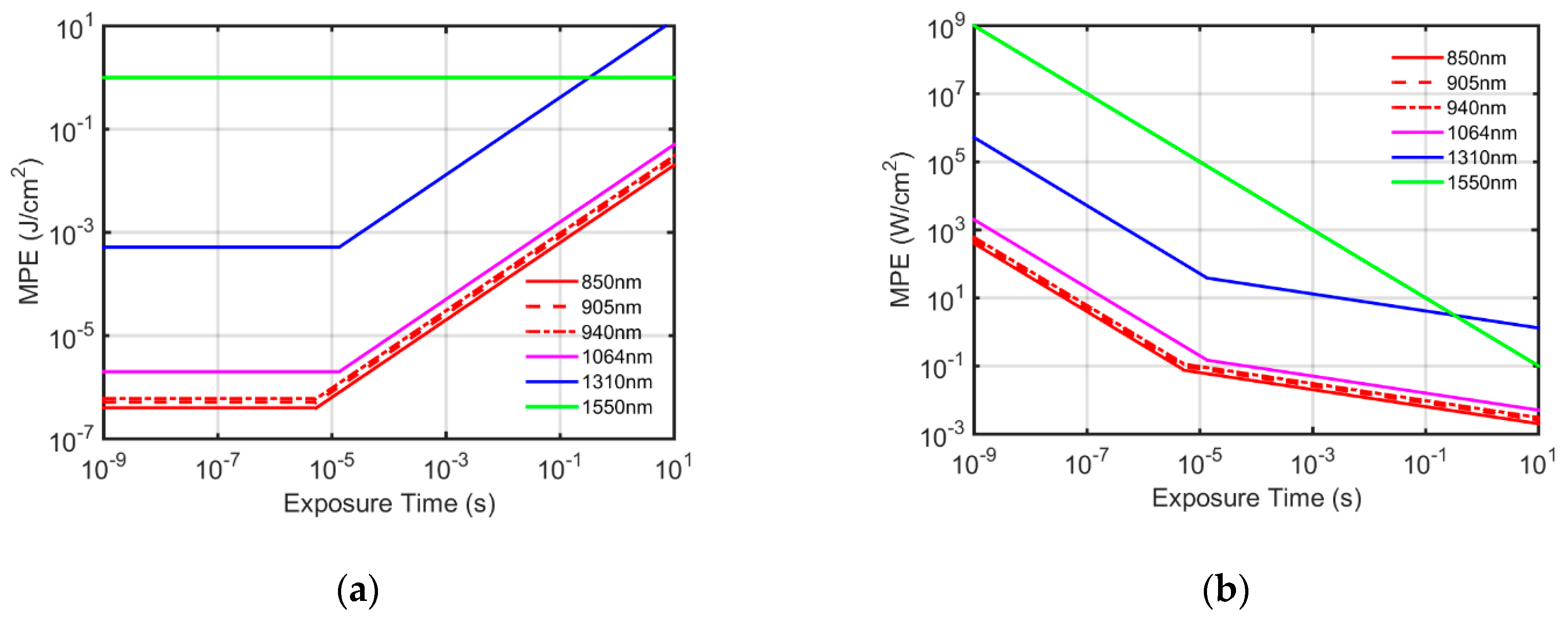
3.2.1. Eye Safety
3.2.2. Waveguiding Material
3.2.3. Lasers and Photodetectors
3.2.4. Ambient Light Suppression
4. Si Photonics Optical Phased Array
4.1. OPA System Design
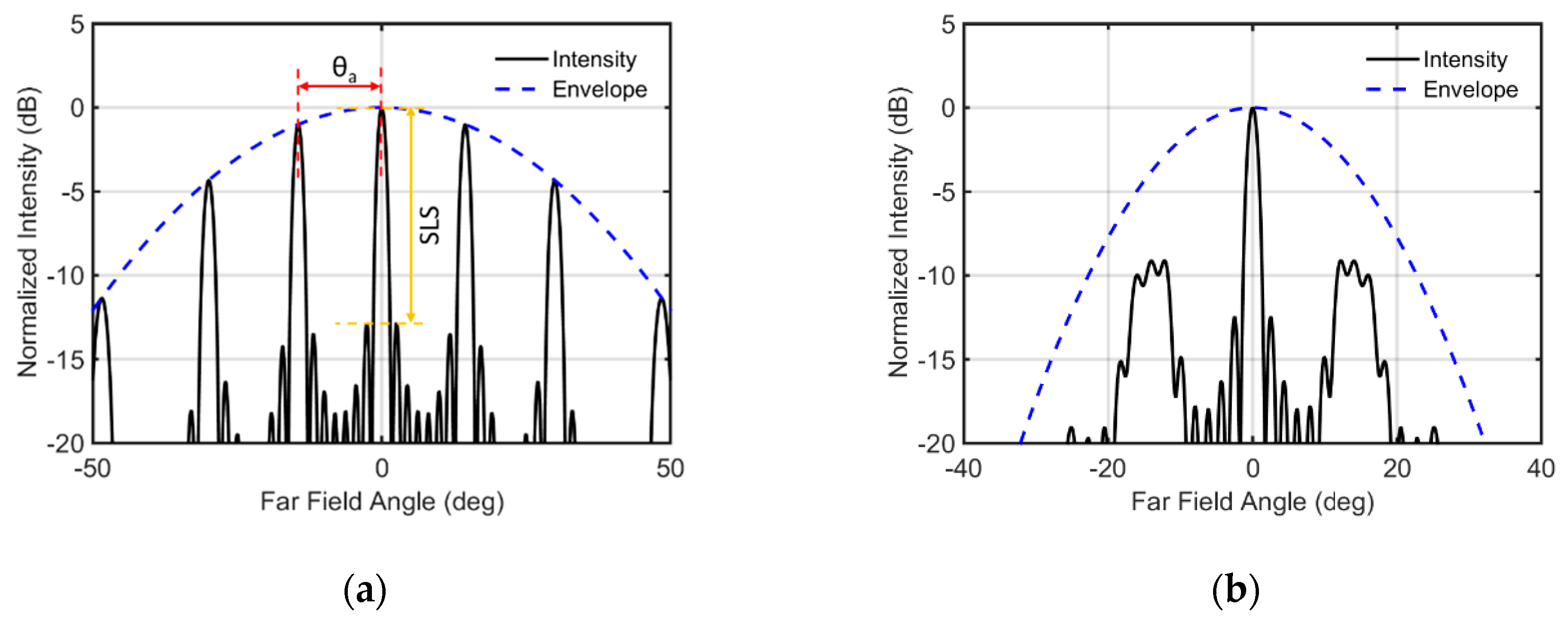
4.1.1. Beam Divergence
4.1.2. Beam Steering Range
4.1.3. 2D Beam Steering
4.2. Key Components
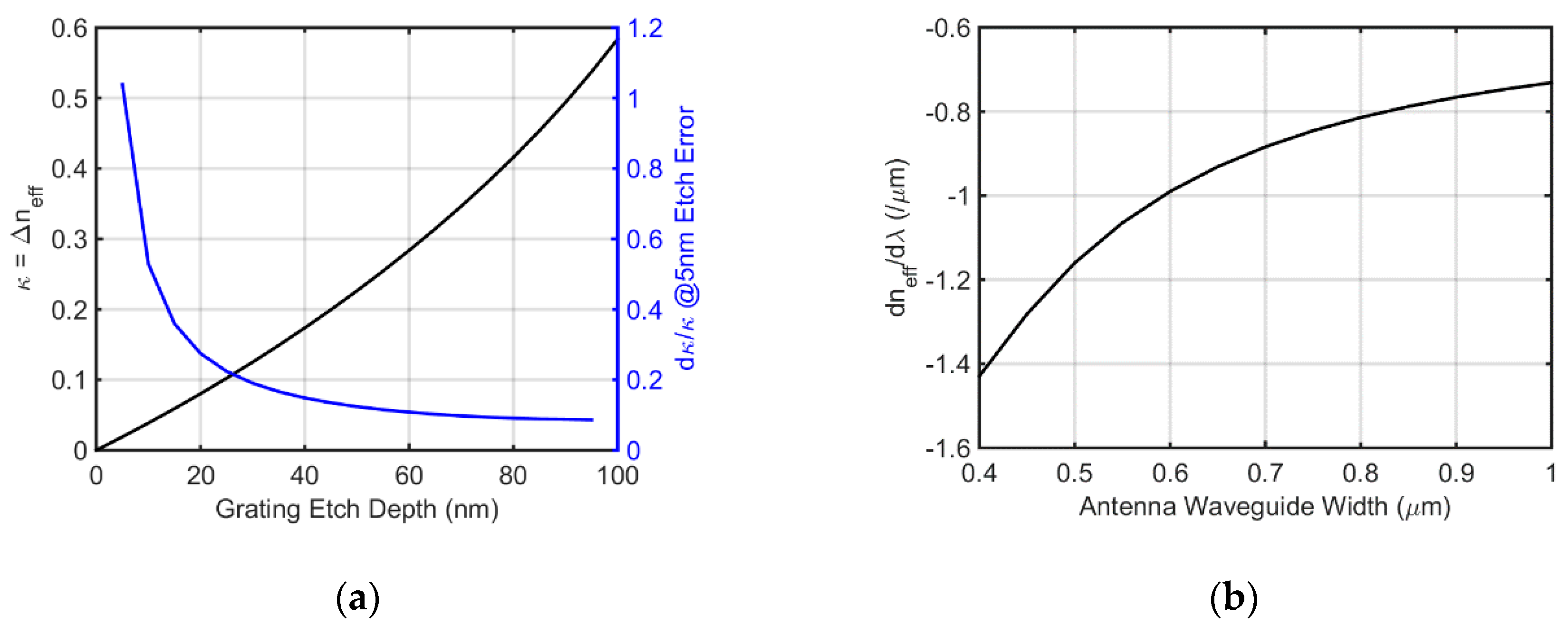
4.2.1. Antenna
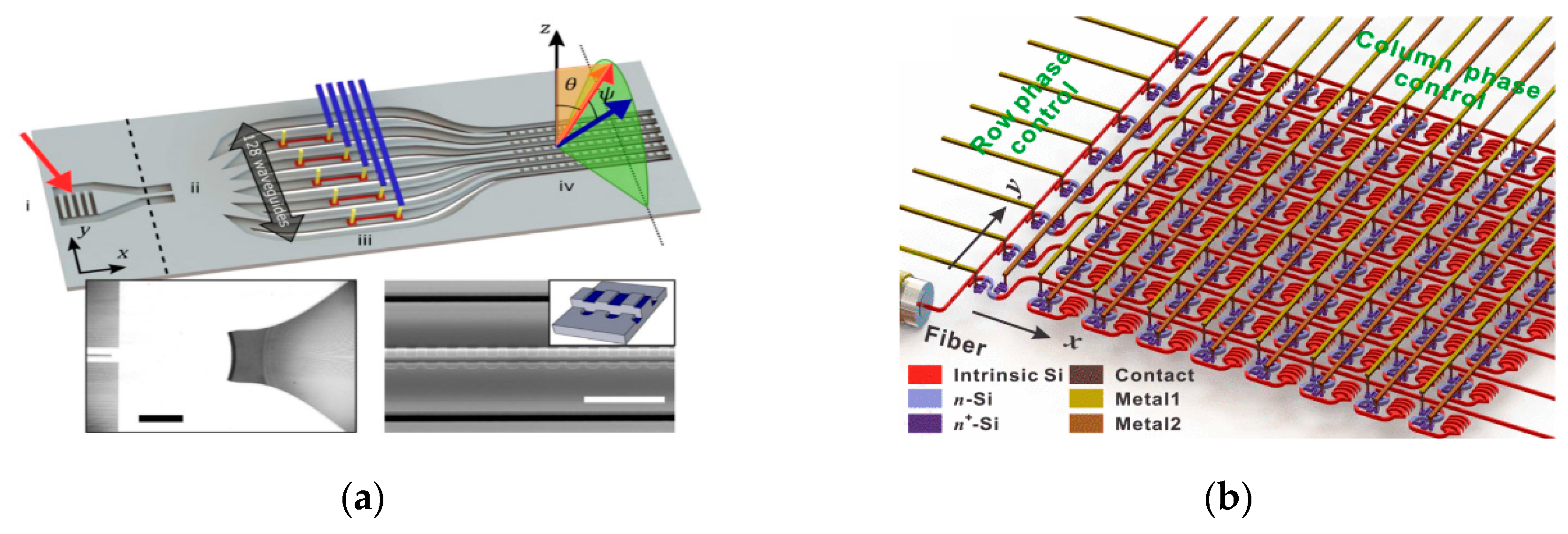
4.2.2. Antenna Array
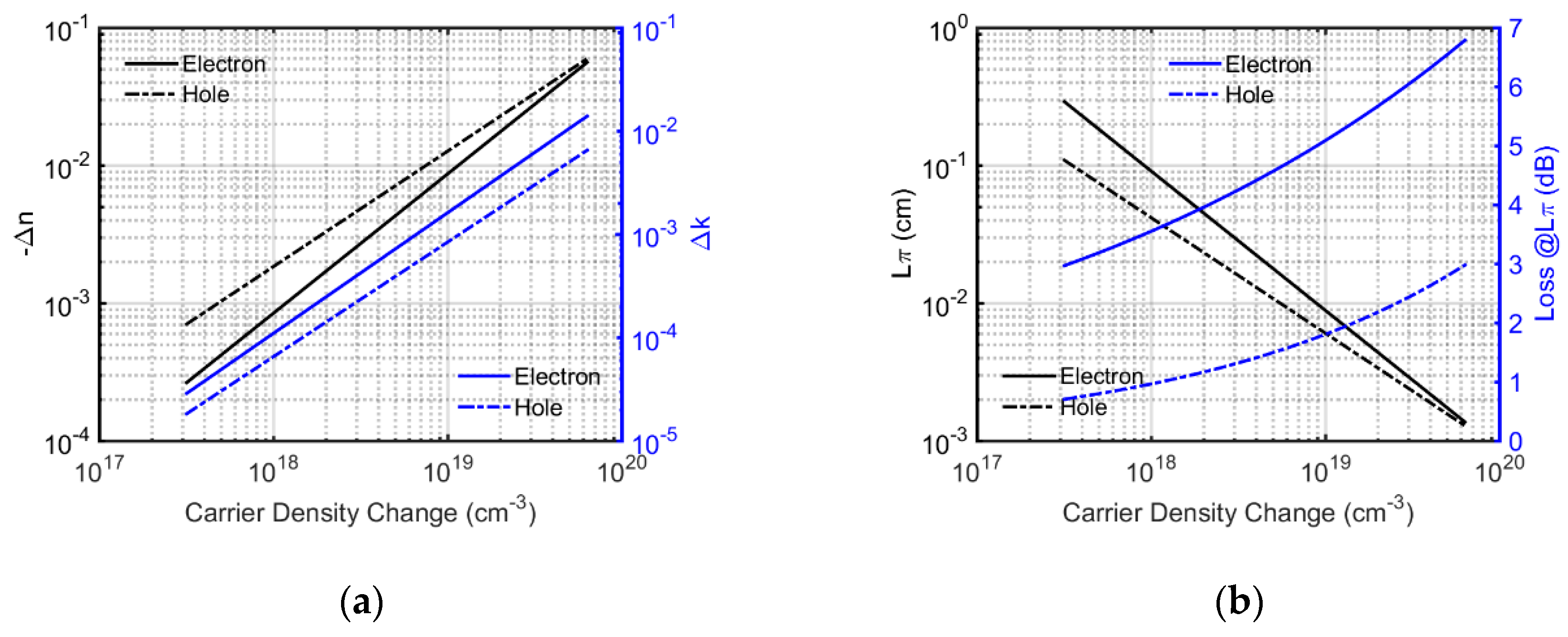
4.2.3. Phase Shifter
5. Other Si Photonics Use Cases for LiDAR
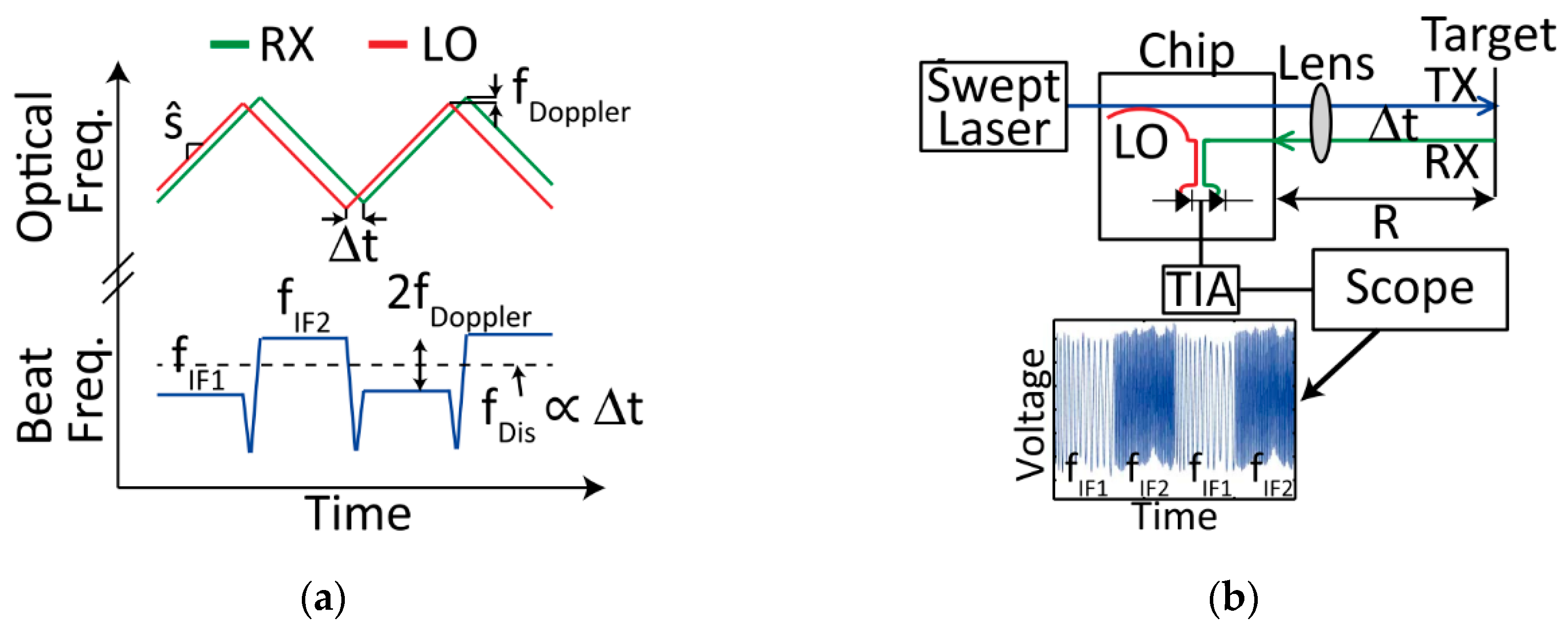
5.1. FMCW Coherent Receiver
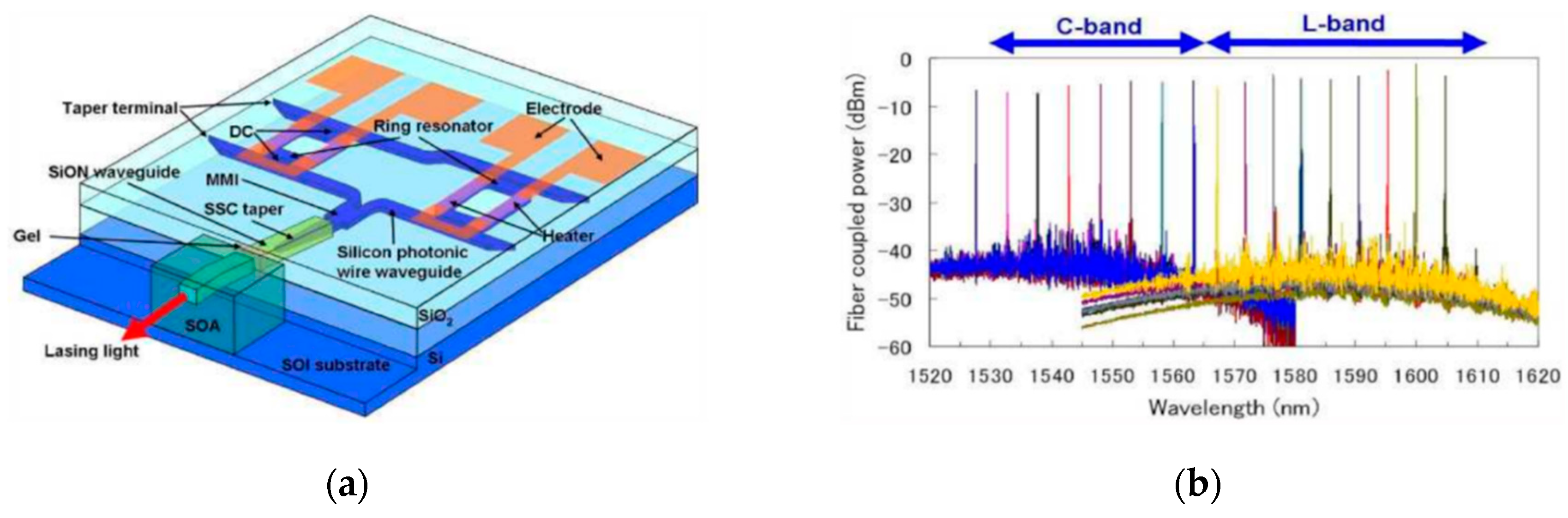
5.2. Narrow Linewidth Tunable Laser
6. Summary
Author Contributions
Funding
Conflicts of Interest
References
- Kirchain, R.; Kimerling, L. A roadmap for nanophotonics. Nat. Photonics 2007, 1, 303. [Google Scholar] [CrossRef]
- Yamada, K.; Tsuchizawa, T.; Nishi, H.; Kou, R.; Hiraki, T.; Takeda, K.; Fukuda, H.; Ishikawa, Y.; Wada, K.; Yamamoto, T. High-performance silicon photonics technology for telecommunications applications. Sci. Technol. Adv. Mater. 2014, 15, 024603. [Google Scholar] [CrossRef] [PubMed]
- Doerr, C. Silicon photonic integration in telecommunications. Front. Phys. 2015, 3. [Google Scholar] [CrossRef]
- Thomson, D.; Zilkie, A.; Bowers, J.E.; Komljenovic, T.; Reed, G.T.; Vivien, L.; Marris-Morini, D.; Cassan, E.; Virot, L.; Fédéli, J.-M.; et al. Roadmap on silicon photonics. J. Opt. 2016, 18, 073003. [Google Scholar] [CrossRef]
- Dong, P.; Melikyan, A.; Kim, K. Silicon photonic integrated circuits for telecom and datacom applications. In Proceedings of the 2018 23rd Opto-Electronics and Communications Conference (OECC), Jeju Island, Korea, 2–6 July 2018; pp. 1–2. [Google Scholar]
- Heck, M. Highly integrated optical phased arrays: Photonic integrated circuits for optical beam shaping and beam steering. Nanophotonics 2016, 6, 93. [Google Scholar] [CrossRef]
- Charbon, E.; Fishburn, M.W. Monolithic Single-Photon Avalanche Diodes: SPADs. In Single-Photon Imaging; Seitz, P., Theuwissen, A.J.P., Eds.; Springer: Berlin/Heidelberg, Germany, 2011; Volume 160, pp. 123–157. ISBN 978-3-642-18443-7. [Google Scholar]
- Süss, A.; Rochus, V.; Rosmeulen, M.; Rottenberg, X. Benchmarking time-of-flight based depth measurement techniques. In Proceedings of the Smart Photonic and Optoelectronic Integrated Circuits XVIII, San Francisco, CA, USA, 3 March 2016; SPIE: Bellingham, WA, USA, 2016; Volume 9751. [Google Scholar]
- Whyte, R.; Streeter, L.; Cree, M.J.; Dorrington, A.A. Application of lidar techniques to time-of-flight range imaging. Appl. Opt. 2015, 54, 9654–9664. [Google Scholar] [CrossRef]
- Valeo 2017 Activity and Sustainable Development Report. Available online: https://www.valeo.com/wp-content/uploads/2018/05/Valeo_Rapport_Annuel_2017_en.pdf (accessed on 5 September 2019).
- Jarvis, A. Velodyne Lidar Press Release, MARCH 28. 2019. Available online: https://velodynelidar.com/newsroom/velodyne-achieves-half-a-billion-dollars-in-lidar-sensors-shipped/ (accessed on 5 September 2019).
- Kawamura, Y.; Wakita, K.; Itaya, Y.; Yoshikuni, Y.; Asahi, H. Monolithic integration of InGaAs/InP DFB lasers and InGaAs/InAlAs MQW optical modulators. Electron. Lett. 1986, 22, 242–243. [Google Scholar] [CrossRef]
- Pulikkaseril, C.; Lam, S. Laser eyes for driverless cars: The road to automotive LIDAR. In Proceedings of the Optical Fiber Communication Conference, Tu3D.2, San Diego, CA, USA, 3–7 March 2019. [Google Scholar]
- Petrovskaya, A.; Thrun, S. Model based vehicle detection and tracking for autonomous urban driving. Auton. Robot. 2009, 26, 123–139. [Google Scholar] [CrossRef]
- McManamon, P.F.; Dorschner, T.A.; Corkum, D.L.; Friedman, L.J.; Hobbs, D.S.; Holz, M.; Liberman, S.; Nguyen, H.Q.; Resler, D.P.; Sharp, R.C.; et al. Optical phased array technology. Proc. Ieee 1996, 84, 268–298. [Google Scholar] [CrossRef]
- Shi, L.; McManamon, P.F.; Bryant, D.; Wall, B.; Groom, M.; Bos, P.J. Beam steering using a liquid crystal optical phase plate with a variable in-plane gradient. In Proceedings of the Frontiers in Optics 2008/Laser Science XXIV/Plasmonics and Metamaterials/Optical Fabrication and Testing, Rochester, NY, USA, 19–23 October 2008; p. FThU7. [Google Scholar]
- Boeuf, F.; Crémer, S.; Vulliet, N.; Pinguet, T.; Mekis, A.; Masini, G.; Verslegers, L.; Sun, P.; Ayazi, A.; Hon, N.; et al. A multi-wavelength 3D-compatible silicon photonics platform on 300 mm SOI wafers for 25Gb/s applications. In Proceedings of the 2013 IEEE International Electron Devices Meeting, Washington, DC, USA, 9–11 December 2013; p. 13. [Google Scholar]
- Lim, A.E.; Tsung-Yang, L.; Junfeng, S.; Chao, L.; Fang, Q.; Xiaoguang, T.; Ning, D.; Kok Kiong, C.; Tern, R.P.C.; Chuan, P.; et al. Path to silicon photonics commercialization: 25 Gb/s platform development in a CMOS manufacturing foundry line. In Proceedings of the OFC 2014, San Francisco, CA, USA, 9–13 March 2014; pp. 1–3. [Google Scholar]
- Absil, P.P.; Verheyen, P.; De Heyn, P.; Pantouvaki, M.; Lepage, G.; De Coster, J.; Van Campenhout, J. Silicon photonics integrated circuits: A manufacturing platform for high density, low power optical I/O’s. Opt. Express 2015, 23, 9369–9378. [Google Scholar] [CrossRef]
- Mogami, T.; Horikawa, T.; Kinoshita, K.; Sasaki, H.; Morito, K.; Kurata, K. A 300 mm Si photonics platform for optical interconnection. In Proceedings of the 2015 IEEE International Interconnect Technology Conference and 2015 IEEE Materials for Advanced Metallization Conference (IITC/MAM), Grenoble, France, 18–21 May 2015; pp. 273–276. [Google Scholar]
- Rahim, A.; Spuesens, T.; Baets, R.; Bogaerts, W. Open-Access Silicon Photonics: Current Status and Emerging Initiatives. Proc. IEEE 2018, 106, 2313–2330. [Google Scholar] [CrossRef]
- Giewont, K.; Nummy, K.; Anderson, F.A.; Ayala, J.; Barwicz, T.; Bian, Y.; Dezfulian, K.K.; Gill, D.M.; Houghton, T.; Hu, S.; et al. 300-mm Monolithic Silicon Photonics Foundry Technology. IEEE J. Sel. Top. Quantum Electron. 2019, 25, 1–11. [Google Scholar] [CrossRef]
- Szelag, B.; Blampey, B.; Ferrotti, T.; Reboud, V.; Hassan, K.; Malhouitre, S.; Grand, G.; Fowler, D.; Brision, S.; Bria, T.; et al. Multiple wavelength silicon photonic 200 mm R+D platform for 25 Gb/s and above applications. In Proceedings of the Silicon Photonics and Photonic Integrated Circuits V, Brussels, Belgium, 13 May 2016; SPIE: Bellingham, WA, USA, 2016; Volume 9891. [Google Scholar]
- Boeuf, F.; Crémer, S.; Temporiti, E.; Ferè, M.; Shaw, M.; Baudot, C.; Vulliet, N.; Pinguet, T.; Mekis, A.; Masini, G.; et al. Silicon Photonics R&D and Manufacturing on 300-mm Wafer Platform. J. Lightwave Technol. 2016, 34, 286–295. [Google Scholar] [CrossRef]
- Rahim, A.; Ryckeboer, E.; Subramanian, A.Z.; Clemmen, S.; Kuyken, B.; Dhakal, A.; Raza, A.; Hermans, A.; Muneeb, M.; Dhoore, S.; et al. Expanding the Silicon Photonics Portfolio with Silicon Nitride Photonic Integrated Circuits. J. Lightwave Technol. 2017, 35, 639–649. [Google Scholar] [CrossRef]
- Wilmart, Q.; el Dirani, H.; Tyler, N.; Fowler, D.; Malhouitre, S.; Garcia, S.; Casale, M.; Kerdiles, S.; Hassan, K.; Monat, C.; et al. A Versatile Silicon-Silicon Nitride Photonics Platform for Enhanced Functionalities and Applications. Appl. Sci. 2019, 9, 255. [Google Scholar] [CrossRef]
- Muñoz, P.; Micó, G.; Bru, A.L.; Pastor, D.; Pérez, D.; Doménech, D.J.; Fernández, J.; Baños, R.; Gargallo, B.; Alemany, R.; et al. Silicon Nitride Photonic Integration Platforms for Visible, Near-Infrared and Mid-Infrared Applications. Sensors 2017, 17, 2088. [Google Scholar] [CrossRef] [PubMed]
- Blumenthal, D.J.; Heideman, R.; Geuzebroek, D.; Leinse, A.; Roeloffzen, C. Silicon Nitride in Silicon Photonics. Proc. IEEE 2018, 106, 2209–2231. [Google Scholar] [CrossRef]
- Zilkie, A.J.; Srinivasan, P.; Trita, A.; Schrans, T.; Yu, G.; Byrd, J.; Nelson, D.A.; Muth, K.; Lerose, D.; Alalusi, M.; et al. Multi-Micron Silicon Photonics Platform for Highly Manufacturable and Versatile Photonic Integrated Circuits. IEEE J. Sel. Top. Quantum Electron. 2019, 25, 1–13. [Google Scholar] [CrossRef]
- Elshaari, A.W.; Zadeh, I.E.; Jöns, K.D.; Zwiller, V. Thermo-Optic Characterization of Silicon Nitride Resonators for Cryogenic Photonic Circuits. IEEE Photonics J. 2016, 8, 1–9. [Google Scholar] [CrossRef]
- Zanatta, A.R.; Gallo, I.B. The Thermo Optic Coefficient of Amorphous SiN Films in the Near-Infrared and Visible Regions and Its Experimental Determination. Appl. Phys. Express 2013, 6, 042402. [Google Scholar] [CrossRef]
- Bristow, A.D.; Rotenberg, N.; van Driel, H.M. Two-photon absorption and Kerr coefficients of silicon for 850–2200 nm. Appl. Phys. Lett. 2007, 90, 191104. [Google Scholar] [CrossRef]
- Ikeda, K.; Saperstein, R.E.; Alic, N.; Fainman, Y. Thermal and Kerr nonlinear properties of plasma-deposited silicon nitride/silicon dioxide waveguides. Opt. Express 2008, 16, 12987–12994. [Google Scholar] [CrossRef]
- Wang, L.; Xie, W.; Van Thourhout, D.; Zhang, Y.; Yu, H.; Wang, S. Nonlinear silicon nitride waveguides based on a PECVD deposition platform. Opt. Express 2018, 26, 9645–9654. [Google Scholar] [CrossRef]
- Levy, J.S.; Gondarenko, A.; Foster, M.A.; Turner-Foster, A.C.; Gaeta, A.L.; Lipson, M. CMOS-compatible multiple-wavelength oscillator for on-chip optical interconnects. Nat. Photonics 2009, 4, 37. [Google Scholar] [CrossRef]
- Smith, R.G. Optical Power Handling Capacity of Low Loss Optical Fibers as Determined by Stimulated Raman and Brillouin Scattering. Appl. Opt. 1972, 11, 2489–2494. [Google Scholar] [CrossRef] [PubMed]
- Komma, J.; Schwarz, C.; Hofmann, G.; Heinert, D.; Nawrodt, R. Thermo-optic coefficient of silicon at 1550 nm and cryogenic temperatures. Appl. Phys. Lett. 2012, 101, 041905. [Google Scholar] [CrossRef]
- Rong, H.; Liu, A.; Jones, R.; Cohen, O.; Hak, D.; Nicolaescu, R.; Fang, A.; Paniccia, M. An all-silicon Raman laser. Nature 2005, 433, 292–294. [Google Scholar] [CrossRef]
- Lin, Q.; Painter, O.J.; Agrawal, G.P. Nonlinear optical phenomena in silicon waveguides: Modeling and applications. Opt. Express 2007, 15, 16604–16644. [Google Scholar] [CrossRef]
- Fisher, E.M.D. Principles and Early Historical Development of Silicon Avalanche and Geiger-Mode Photodiodes; Photon Counting—Fundamentals and Applications; Britun, N., Nikiforov, A., Eds.; IntechOpen: London, UK, 2017; ISBN 978-953-51-3908-9. [Google Scholar]
- Technology, Quanergy Systems, Inc. Available online: https://quanergy.com/technology-2/ (accessed on 5 September 2019).
- Automotive LiDAR Market Report from Woodside Capital Partners and Yole Développement, April 2018. Available online: https://www.osa.org/en-us/industry/industry_intelligence/publications_reports/automotive_lidar_market_report/ (accessed on 5 September 2019).
- Martin, A.; Dodane, D.; Leviandier, L.; Dolfi, D.; Naughton, A.; O’Brien, P.; Spuessens, T.; Baets, R.; Lepage, G.; Verheyen, P.; et al. Photonic Integrated Circuit-Based FMCW Coherent LiDAR. J. Lightwave Technol. 2018, 36, 4640–4645. [Google Scholar] [CrossRef]
- Blackmore Sensors and Analytics, Inc. Available online: https://blackmoreinc.com (accessed on 5 September 2019).
- Analog Photonics LLC. Available online: http://www.analogphotonics.com/ (accessed on 5 September 2019).
- ASTM G173-03(2012). Available online: http://www.astm.org/cgi-bin/resolver.cgi?G173-03(2012) (accessed on 5 September 2019).
- Vasey, F.; Reinhart, F.K.; Houdré, R.; Stauffer, J.M. Spatial optical beam steering with an AlGaAs integrated phased array. Appl. Opt. 1993, 32, 3220–3232. [Google Scholar] [CrossRef]
- Van Acoleyen, K.; Bogaerts, W.; Jágerská, J.; Le Thomas, N.; Houdré, R.; Baets, R. Off-chip beam steering with a one-dimensional optical phased array on silicon-on-insulator. Opt. Lett. 2009, 34, 1477–1479. [Google Scholar] [CrossRef] [PubMed]
- Van Acoleyen, K.; Rogier, H.; Baets, R. Two-dimensional optical phased array antenna on silicon-on-insulator. Opt. Express 2010, 18, 13655–13660. [Google Scholar] [CrossRef] [PubMed]
- Doylend, J.K.; Heck, M.J.R.; Bovington, J.T.; Peters, J.D.; Coldren, L.A.; Bowers, J.E. Two-dimensional free-space beam steering with an optical phased array on silicon-on-insulator. Opt. Express 2011, 19, 21595–21604. [Google Scholar] [CrossRef] [PubMed]
- Doylend, J.; Heck, M.R.; Bovington, J.; Peters, J.; Coldren, L.; Bowers, J. Free-space Beam Steering in Two Dimensions Using a Silicon Optical Phased Array. In Proceedings of the Optical Fiber Communication Conference, Los Angeles, CA, USA, 4–8 March 2012; p. OM2J.1. [Google Scholar]
- Kwong, D.; Hosseini, A.; Zhang, Y.; Chen, R.T. 1 × 12 Unequally spaced waveguide array for actively tuned optical phased array on a silicon nanomembrane. Appl. Phys. Lett. 2011, 99, 051104. [Google Scholar] [CrossRef]
- Doylend, J.K.; Heck, M.J.R.; Bovington, J.T.; Peters, J.D.; Davenport, M.L.; Coldren, L.A.; Bowers, J.E. Hybrid III/V silicon photonic source with integrated 1D free-space beam steering. Opt. Lett. 2012, 37, 4257–4259. [Google Scholar] [CrossRef] [PubMed]
- Sun, J.; Timurdogan, E.; Yaacobi, A.; Su, Z.; Hosseini, E.S.; Cole, D.B.; Watts, M.R. Large-Scale Silicon Photonic Circuits for Optical Phased Arrays. IEEE J. Sel. Top. Quantum Electron. 2014, 20, 264–278. [Google Scholar] [CrossRef]
- Guo, W.; Binetti, P.R.A.; Masanovic, M.L.; Johansson, L.A.; Coldren, L.A. Large-scale InP photonic integrated circuit packaged with ball grid array for 2D optical beam steering. In Proceedings of the 2013 IEEE Photonics Conference, Bellevue, WA, USA, 8–12 September 2013; pp. 651–652. [Google Scholar]
- Abiri, B.; Aflatouni, F.; Rekhi, A.; Hajimiri, A. Electronic Two-Dimensional Beam Steering for Integrated Optical Phased Arrays. In Proceedings of the Optical Fiber Communication Conference, San Francisco, CA, USA, 9–14 March 2014; p. M2K.7. [Google Scholar]
- Yaacobi, A.; Sun, J.; Moresco, M.; Leake, G.; Coolbaugh, D.; Watts, M.R. On chip wide angle beam steering. In Proceedings of the 2014 Conference on Lasers and Electro-Optics (CLEO)—Laser Science to Photonic Applications, San Jose, CA, USA, 8–13 June 2014; pp. 1–2. [Google Scholar]
- Yaacobi, A.; Sun, J.; Moresco, M.; Leake, G.; Coolbaugh, D.; Watts, M.R. Integrated phased array for wide-angle beam steering. Opt. Lett. 2014, 39, 4575–4578. [Google Scholar] [CrossRef]
- Kwong, D.; Hosseini, A.; Covey, J.; Zhang, Y.; Xu, X.; Subbaraman, H.; Chen, R.T. On-chip silicon optical phased array for two-dimensional beam steering. Opt. Lett. 2014, 39, 941–944. [Google Scholar] [CrossRef]
- Hulme, J.C.; Doylend, J.K.; Heck, M.J.R.; Peters, J.D.; Davenport, M.L.; Bovington, J.T.; Coldren, L.A.; Bowers, J.E. Fully integrated hybrid silicon free-space beam steering source with 32-channel phased array. In Proceedings of the Smart Photonic and Optoelectronic Integrated Circuits XVI, Santa Barbara, CA, USA, 8 March 2014; SPIE: Bellingham, WA, USA, 2014; Volume 8989. [Google Scholar]
- Hulme, J.C.; Doylend, J.K.; Heck, M.J.R.; Peters, J.D.; Davenport, M.L.; Bovington, J.T.; Coldren, L.A.; Bowers, J.E. Fully integrated hybrid silicon two dimensional beam scanner. Opt. Express 2015, 23, 5861–5874. [Google Scholar] [CrossRef]
- Abediasl, H.; Hashemi, H. Monolithic optical phased-array transceiver in a standard SOI CMOS process. Opt. Express 2015, 23, 6509–6519. [Google Scholar] [CrossRef]
- Poulton, C.V.; Yaacobi, A.; Su, Z.; Byrd, M.J.; Watts, M.R. Optical Phased Array with Small Spot Size, High Steering Range and Grouped Cascaded Phase Shifters. In Proceedings of the Advanced Photonics 2016 (IPR, NOMA, Sensors, Networks, SPPCom, SOF), Vancouver, BC, Canada, 18–20 July 2016; p. IW1B.2. [Google Scholar]
- Poulton, C.V.; Yaacobi, A.; Cole, D.B.; Byrd, M.J.; Raval, M.; Vermeulen, D.; Watts, M.R. Coherent solid-state LIDAR with silicon photonic optical phased arrays. Opt. Lett. 2017, 42, 4091–4094. [Google Scholar] [CrossRef] [PubMed]
- Hutchison, D.N.; Sun, J.; Doylend, J.K.; Kumar, R.; Heck, J.; Kim, W.; Phare, C.T.; Feshali, A.; Rong, H. High-resolution aliasing-free optical beam steering. Optica 2016, 3, 887–890. [Google Scholar] [CrossRef]
- Poulton, C.V.; Byrd, M.J.; Raval, M.; Su, Z.; Li, N.; Timurdogan, E.; Coolbaugh, D.; Vermeulen, D.; Watts, M.R. Large-scale silicon nitride nanophotonic phased arrays at infrared and visible wavelengths. Opt. Lett. 2017, 42, 21–24. [Google Scholar] [CrossRef] [PubMed]
- Zhao, C.; Zhang, H.; Zheng, Z.; Peng, C.; Hu, W. Silicon optical-phased-array prototypes using electro-optical phase shifters. In Proceedings of the 2017 Conference on Lasers and Electro-Optics (CLEO), San Jose, CA, USA, 14–19 May 2017; pp. 1–2. [Google Scholar]
- Miller, S.A.; Phare, C.T.; Chang, Y.; Ji, X.; Gordillo, O.A.J.; Mohanty, A.; Roberts, S.P.; Shin, M.C.; Stern, B.; Zadka, M.; et al. 512-Element Actively Steered Silicon Phased Array for Low-Power LIDAR. In Proceedings of the 2018 Conference on Lasers and Electro-Optics (CLEO), San Jose, CA, USA, 13–18 May 2018; pp. 1–2. [Google Scholar]
- Phare, C.T.; Shin, M.C.; Sharma, J.; Ahasan, S.; Krishnaswamy, H.; Lipson, M. Silicon Optical Phased Array with Grating Lobe-Free Beam Formation over 180 Degree Field of View. In Proceedings of the 2018 Conference on Lasers and Electro-Optics (CLEO), San Jose, CA, USA, 13–18 May 2018; pp. 1–2. [Google Scholar]
- Chung, S.; Abediasl, H.; Hashemi, H. A Monolithically Integrated Large-Scale Optical Phased Array in Silicon-on-Insulator CMOS. IEEE J. Solid-State Circuits 2018, 53, 275–296. [Google Scholar] [CrossRef]
- Tyler, N.A.; Fowler, D.; Malhouitre, S.; Garcia, S.; Grosse, P.; Rabaud, W.; Szelag, B. SiN integrated optical phased arrays for two-dimensional beam steering at a single near-infrared wavelength. Opt. Express 2019, 27, 5851–5858. [Google Scholar] [CrossRef] [PubMed]
- Zhang, Y.; Ling, Y.-C.; Zhang, K.; Gentry, C.; Sadighi, D.; Whaley, G.; Colosimo, J.; Suni, P.; Ben Yoo, S.J. Sub-wavelength-pitch silicon-photonic optical phased array for large field-of-regard coherent optical beam steering. Opt. Express 2019, 27, 1929–1940. [Google Scholar] [CrossRef] [PubMed]
- Bandres, M.A.; Gutiérrez-Vega, J.C. Ince–Gaussian beams. Opt. Lett. 2004, 29, 144–146. [Google Scholar] [CrossRef]
- HR80 Series, Cepton Technologies, Inc. Available online: https://www.cepton.com/hr80.html (accessed on 5 September 2019).
- Christopher Palmer and Erwin Loewen, Diffraction Grating Handbook, Newport Corp. Available online: http://www.newport.com (accessed on 5 September 2019).
- Zadka, M.; Chang, Y.-C.; Mohanty, A.; Phare, C.T.; Roberts, S.P.; Lipson, M. On-chip platform for a phased array with minimal beam divergence and wide field-of-view. Opt. Express 2018, 26, 2528–2534. [Google Scholar] [CrossRef]
- Parriaux, O.; Sychugov, V.A.; Tishchenko, A.V. Coupling gratings as waveguide functional elements. Pure Appl. Opt. 1996, 5, 453. [Google Scholar] [CrossRef]
- Komljenovic, T.; Helkey, R.; Coldren, L.; Bowers, J.E. Sparse aperiodic arrays for optical beam forming and LIDAR. Opt. Express 2017, 25, 2511–2528. [Google Scholar] [CrossRef]
- Zhang, L.; Sun, X.; Zhang, W.; Wang, G.; Feng, N.; Zhao, W. Compact optical phased array using a serial grating antenna design. arXiv 2019, arXiv:1903.04573. [Google Scholar]
- Soref, R.; Bennett, B. Electrooptical effects in silicon. IEEE J. Quantum Electron. 1987, 23, 123–129. [Google Scholar] [CrossRef]
- Nedeljkovic, M.; Soref, R.; Mashanovich, G.Z. Free-Carrier Electrorefraction and Electroabsorption Modulation Predictions for Silicon Over the 1–14- μm Infrared Wavelength Range. IEEE Photonics J. 2011, 3, 1171–1180. [Google Scholar] [CrossRef]
- Doerr, C.R.; Winzer, P.J.; Chen, Y.; Chandrasekhar, S.; Rasras, M.S.; Chen, L.; Liow, T.; Ang, K.; Lo, G. Monolithic Polarization and Phase Diversity Coherent Receiver in Silicon. J. Lightwave Technol. 2010, 28, 520–525. [Google Scholar] [CrossRef]
- Doerr, C.; Chen, L.; Vermeulen, D.; Nielsen, T.; Azemati, S.; Stulz, S.; McBrien, G.; Xu, X.M.; Mikkelsen, B.; Givehchi, M.; et al. Single-Chip Silicon Photonics 100-Gb/s Coherent Transceiver. In Proceedings of the Optical Fiber Communication Conference: Postdeadline Papers, San Francisco, CA, USA, 9–13 March 2014; p. Th5C.1. [Google Scholar]
- Schmitt, J.M. Optical coherence tomography (OCT): A review. IEEE J. Sel. Top. Quantum Electron. 1999, 5, 1205–1215. [Google Scholar] [CrossRef]
- Kim, T.; Bhargava, P.; Stojanović, V. Overcoming the Coherence Distance Barrier in Long-Range FMCW LIDAR. In Proceedings of the 2018 Conference on Lasers and Electro-Optics (CLEO), San Jose, CA, USA, 13–18 May 2018; pp. 1–2. [Google Scholar]
- Hariyama, T.; Sandborn, P.A.M.; Watanabe, M.; Wu, M.C. High-accuracy range-sensing system based on FMCW using low-cost VCSEL. Opt. Express 2018, 26, 9285–9297. [Google Scholar] [CrossRef] [PubMed]
- Chu, T.; Fujioka, N.; Ishizaka, M. Compact, lower-power-consumption wavelength tunable laser fabricated with silicon photonic wire waveguide micro-ring resonators. Opt. Express 2009, 17, 14063–14068. [Google Scholar] [CrossRef] [PubMed]
- Koch, B.R.; Norberg, E.J.; Kim, B.; Hutchinson, J.; Shin, J.-H.; Fish, G.; Fang, A. Integrated Silicon Photonic Laser Sources for Telecom and Datacom. In Proceedings of the Optical Fiber Communication Conference/National Fiber Optic Engineers Conference 2013, Anaheim, CA, USA, 17–21 March 2013; p. PDP5C.8. [Google Scholar]
- Kita, T.; Tang, R.; Yamada, H. Narrow Spectral Linewidth Silicon Photonic Wavelength Tunable Laser Diode for Digital Coherent Communication System. IEEE J. Sel. Top. Quantum Electron. 2016, 22, 23–34. [Google Scholar] [CrossRef]


| Distance Calculation | |||||
|---|---|---|---|---|---|
| Time-of-Flight | FMCW (Optical Freq. Chirp) | ||||
| Direct | Indirect (Modulated CW) | ||||
| Pulsed | AM (RF Phase Shift) | FM (RF Freq. Chirp) | |||
| Mapping | Mech. Scan | Production | / | / | R&D |
| MEMS Scan | Early Prod. | R&D | / | R&D | |
| Imaging | Production | Production | R&D | / | |
| OPA | R&D | / | / | R&D | |
| SLM | R&D | / | / | / | |
| Items | Specs | Conditions |
|---|---|---|
| Range | >200 m | 10% reflectivity |
| Horizontal FOV | >120° | / |
| Vertical FOV | >25° | / |
| Angular resolution | <0.1° | / |
| Frame rate | >15 Hz | / |
| Transparency µm | Thickness µm | Loss dB/cm | Bending µm | βTO/K | n2 cm2/GW | βTPA cm/GW | |
|---|---|---|---|---|---|---|---|
| Si | 1.1~3.7 | 0.2~0.5 1 | 1~3 1 | 5~50 1 | 1.8 × 10⁻⁴ 2 | 5 × 10⁻⁵ 2 | 0.5 2 |
| SiN | 0.5~3.7 | 0.2~2 1 | 0.2~2 1 | 20~200 1 | 2~4 × 10⁻⁵ 2 | 3~7 × 10⁻⁶ 2 | neg. |
| Wavelength (nm) | Lasers | Photodetectors |
|---|---|---|
| 850, 905, 940 | VCSEL, EEL | Si PD/APD/SPAD |
| 1064 | DPSSL | Si SPAD |
| 1310 | EEL | InGaAs PD/APD |
| 1550 | EEL (+EDFA), fiber laser | InGaAs PD/APD |
| Ref. | Yr | Group | Ant. | Nan | Dan µm | Beam deg | Steer. deg | SLS 3 dB | PS/St. | Pπ mW | BW kHz |
|---|---|---|---|---|---|---|---|---|---|---|---|
| [48] | 09 | UGent | LG | 16 | 2 | 2.7, 2.5 | 50, 0.14 1 | TO + λ | 8.2 | ||
| [49] | 10 | UGent | FG | 4 × 4 | 60 | 0.4, 0.4 | 0.2 1 | λ | |||
| [50,51] | 11 | UCSB | LG | 16 | 3.5 | 0.6, 1.6 | 20, 0.14 1 | 10 | TO + λ | 215 | |
| [52] | 11 | UTA | EE | 12 | 3.1 2 | 32 | 2–7 | TO | 12 | 100 | |
| [53] | 12 | UCSB | LG | 8 | 5.5 | 1.8, 0.6 | 12 | 7 | TO | 97 | |
| [54] | 13 | MIT | FG | 8 × 8 | 9 | 6, 6 | TO | 8.5 | |||
| [55] | 13 | UCSB 4 | LG | 32 | 0.3, 1.2 | 35, 0.14 1 | 15 | CI+λ | 1 × 10⁴ | ||
| [56] | 14 | Caltech | FG | 4 × 4 | 50 | 0.5, 0.5 | 1.8, 1.8 | CI | >10 | ||
| [57,58] | 14 | MIT | LG | 16 | 2 | 51 | TO | 13 | 100 | ||
| [59] | 14 | UTA | LG | 16 | 4 | 1.2, 0.5 | 20, 0.15 1 | 6–10 | TO + λ | 20 | 7.3 |
| [60] | 14 | UCSB 4 | LG | 32 | 0.6, 0.6 | 15, 0.14 1 | 15 | CI+λ | >14 | 4 × 10³ | |
| [61] | 15 | UCSB 4 | LG | 32 | 3.4 2 | 1, 0.6 | 23, 0.13 1 | 8–14 | CI+λ | >14 | 5 × 10⁴ |
| [62] | 15 | USC | FG | 8 × 8 | 33 | 1.6 | 11 | 14 | |||
| [63,64] | 16 | MIT | LGS | 50 | 2 | 0.9, 0.2 | 46, 0.19 1 | 8 | TO + λ | 13 | |
| [65] | 16 | Intel | LG | 128 | ~2 2 | 0.14, 0.1 | 80 | 8–10 | TO | ||
| [66] | 17 | MIT 5 | LG | 1024 | 4 | 0.02, 0.02 | 46, | 10 | n.a. | ||
| [67] | 17 | PKU | LG | 6 | 8 | 1.5 | 11 | EO | n.a. | 2 × 10⁵ | |
| [68] | 18 | UCol | LGS | 512 | 1.3 | 0.15 | 70, 0.3 1 | 8 | TO + λ | 2.6 | |
| [69] | 18 | UCol | LG | 64 | 0.8 | 1.2 | 120 | 11 | TO | ||
| [70] | 18 | USC | FG | 1024 | 2 | 0.03 | 45 | 9 | TO | 54 | 5 |
| [71] | 19 | Leti 5 | LG | 4, 4 | 3 | 4.3, 0.7 | 17, | TO | 88 | ||
| [72] | 19 | UCD | LGN | 24 | 1.3 | 40, 0.16 1 | TO | 11 |
© 2019 by the authors. Licensee MDPI, Basel, Switzerland. This article is an open access article distributed under the terms and conditions of the Creative Commons Attribution (CC BY) license (http://creativecommons.org/licenses/by/4.0/).
Share and Cite
Sun, X.; Zhang, L.; Zhang, Q.; Zhang, W. Si Photonics for Practical LiDAR Solutions. Appl. Sci. 2019, 9, 4225. https://doi.org/10.3390/app9204225
Sun X, Zhang L, Zhang Q, Zhang W. Si Photonics for Practical LiDAR Solutions. Applied Sciences. 2019; 9(20):4225. https://doi.org/10.3390/app9204225
Chicago/Turabian StyleSun, Xiaochen, Lingxuan Zhang, Qihao Zhang, and Wenfu Zhang. 2019. "Si Photonics for Practical LiDAR Solutions" Applied Sciences 9, no. 20: 4225. https://doi.org/10.3390/app9204225
APA StyleSun, X., Zhang, L., Zhang, Q., & Zhang, W. (2019). Si Photonics for Practical LiDAR Solutions. Applied Sciences, 9(20), 4225. https://doi.org/10.3390/app9204225