Article

Second-Harmonic Generation in Mie-Resonant GaAs Nanowires

by
Domenico de Ceglia
1,*,
Luca Carletti
1,
Maria Antonietta Vincenti
2,
Costantino De Angelis
2 and
Michael Scalora
3
1
Department of Information Engineering, University of Padova, 35131 Padova, Italy
2
Department of Information Engineering, University of Brescia, 25123 Brescia, Italy
3
Charles M. Bowden Research Lab, US Army AMRDEC, Huntsville, AL 35898, USA
*
Author to whom correspondence should be addressed.
Appl. Sci. 2019, 9(16), 3381; https://doi.org/10.3390/app9163381
Submission received: 15 July 2019 / Revised: 8 August 2019 / Accepted: 14 August 2019 / Published: 16 August 2019
(This article belongs to the Special Issue Recent Advances in Plasmonics and Nanophotonics)

Abstract

:
We investigate the enhancement of second-harmonic generation in cylindrical GaAs nanowires. Although these nanostructures confine light in two dimensions, power conversion efficiencies on the order of 10 5 with a pump peak intensity of ~ 1   GW / cm 2 are possible if the pump and the second-harmonic fields are coupled to the Mie-type resonances of the nanowire. We identify a large range of nanowire radii in which a double-resonance condition, i.e., both the pump and the second-harmonic fields excite normal modes of the nanowire, induces a high-quality-factor peak of conversion efficiency. We show that second-harmonic light can be scattered with large efficiency even if the second-harmonic photon energy is larger than 1.42 eV, i.e., the electronic bandgap of GaAs, above which the material is considered opaque. Finally, we evaluate the efficiency of one-photon absorption of second-harmonic light and find that resonant GaAs nanowires absorb second-harmonic light in the near-field region almost at the same rate at which they radiate second-harmonic light in the far-field region.

1. Introduction

Optical and electronic properties of semiconductors such as Si and GaAs are suitable for the development of highly-efficient nonlinear and tunable nanophotonic devices. Semiconductors possess a high refractive index, which is a fundamental requirement to slow-down light and to increase light confinement and field-enhancement at the nano- or sub-wavelength-scale. In addition, semiconductors have low losses at telecom wavelengths, they are chemically and electrically tunable, and they show a strong nonlinear optical response from visible to far-infrared wavelengths. The bulk quadratic nonlinear response is very strong in anisotropic crystals such as GaAs [1], in which a χ ( 2 ) effect is also present at the surface due to crystal-symmetry breaking and electric-field discontinuity [2]. On the other hand, in isotropic crystals such as Si, χ ( 2 ) is only strong on the surface. Cubic nonlinearities are very large both in the bulk of Si and GaAs. Enhanced nonlinear optical effects have been predicted and experimentally observed in a variety of nanoscale structures based on semiconductors: At the band-edge of photonic crystals [3,4,5,6,7], in leaky-mode-resonant gratings or photonic-crystal slabs [8,9,10], and more recently in Mie-resonant nanoantennas [11,12] and metasurfaces [13,14,15,16]. Besides the large nonlinearity, the fabrication processes of nanoscale semiconductor devices are mature and reliable, and in some cases compatible with existing technologies for photonic integrated circuits, e.g., silicon photonics. The recent popularity gained by semiconductors in nonlinear nanophotonics is also due to the modest amount of absorption losses at telecom wavelengths, at photon energies below the electronic bandgap. Indeed, nanostructures based on semiconductors offer an all-dielectric solution for the design of nanophotonic devices with enhanced light–matter interactions [17], and they are considered valid alternatives to plasmonic-based systems [18], especially for nonlinear optics which require high light-intensities and, in particular, for applications in the visible and near-infrared, where metals absorb light more efficiently. It has been shown that the combination of high material nonlinearity, low absorption losses and the presence of Mie resonances in semiconductor nanoparticles creates ideal conditions to induce highly-efficient nonlinear interactions. Conversion efficiencies as high as 10−5 for second-harmonic (SH) generation in AlGaAs nanocylinders [13,14] and 10−6 for third-harmonic (TH) generation in Si nanospheres [11] have been experimentally demonstrated by tuning the pump signal on the magnetic-dipole resonance. SH generation with record-high efficiency has been predicted in AlGaAs resonators that host bound-in-continuum states [19]. Moreover, the possibility to tailor polarization and radiation patterns has been demonstrated for SH light scattered by AlGaAs nanocylinders [20,21]. The key factor to achieve strong nonlinear interactions in semiconductor nanoparticles is to couple light to Mie scattering modes [22]. Nonlinear effects, such as SH and TH generation, have been so far investigated in isolated and arrayed Si- and GaAs-based resonant nanoparticles with three-dimensional (3D) light confinement, such as spheres and finite cylinders (nanodisks or nanopillars). Here we analyze SH generation in Mie-resonant GaAs nanowires, or infinite cylinders. Mie theory is used to describe the response in the linear regime, which is dominated by the normal modes of the nanowire. Next, an average nonlinear susceptibility, derived by the linear Mie-scattering coefficients and normal modes, is introduced to predict the far-field SH scattering efficiency and finite-element simulations are performed to calculate SH light absorption, to examine near fields, and to test the validity of the average nonlinear susceptibility. Although light is confined in only two dimensions, defined by the scattering plane orthogonal to the nanowires’ axis, we show that, if the nanowires are judiciously designed, conversion efficiencies for SH generation are similar to those achievable in nanoparticles with 3D light confinement. Finally, we discuss the role of absorption losses in SH generation, and demonstrate that: (i) Nanowires produce intense SH light even when the SH photon energy is tuned above the electronic bandgap of GaAs, where the material is opaque and it is commonly assumed that harmonic generation is not efficient, and (ii) absorption of SH light is not negligible even when the SH photon energy is tuned below the electronic bandgap of GaAs.

2. Mie Scattering in the Linear Regime and Normal Modes of GaAs Nanowires

The nanowire geometry and the electromagnetic fields have translational invariance in the direction of the nanowire axis ( z axis in our coordinate system) and therefore we analyze linear and nonlinear optical scattering only in the x y plane. Light is incident as a plane wave with either TM polarization (electric field parallel to the scattering x y -plane) or TE polarization (electric field perpendicular to the scattering plane). We assume that the principal axes of the crystal are oriented as follows: x ^ [ 100 ] ,   y ^ [ 010 ] , and z ^ [ 001 ] . The second-order nonlinear tensor contains only elements of type χ i j k ( 2 ) = χ ( 2 ) with i j k , so that the nonlinear current induced at the SH frequency can be written as:
( J x N L J y N L J z N L ) = i 2 ω p ϵ 0 χ ( 2 ) ( E y p E z p E x p E z p E x p E y p ) ,
where ω p is the pump angular frequency, E x , y , z p indicate the pump electric-field components, and J x , y , z N L 
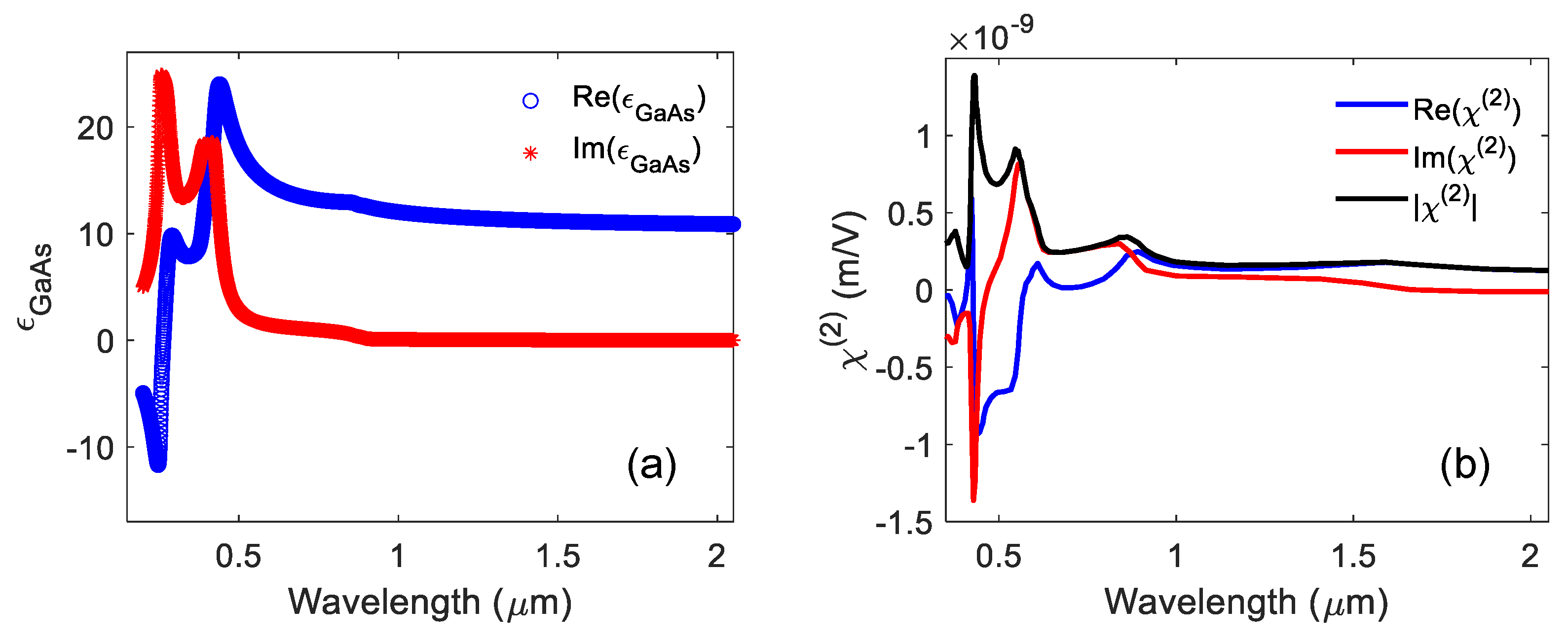
indicate the SH induced current components. Both the relative permittivity of GaAs, ϵ G a A s , and the nonlinear susceptibility χ ( 2 ) are weakly dispersive at infrared wavelengths, in particular for photon energies smaller than the GaAs energy bandgap, E g = h c λ B G = 1.42   eV , where λ B G 870   nm . The frequency-dependence becomes significant at shorter wavelengths ( λ λ B G ), where interband transitions play a non-trivial role in the spectra of SH light scattering and absorption. In Figure 1, we plot the real and imaginary parts of ϵ G a A s and χ ( 2 ) that we use for calculations of linear and nonlinear scattering and absorption efficiencies. Linear and nonlinear optical data are taken from [23,24,25,26], respectively. Both models account for the electronic band structure of GaAs, and therefore they include the E 0 , E 0 + Δ 0 ,   E 1 , E 1 + Δ 1 ,   E 0 , and E 2 transitions of GaAs.
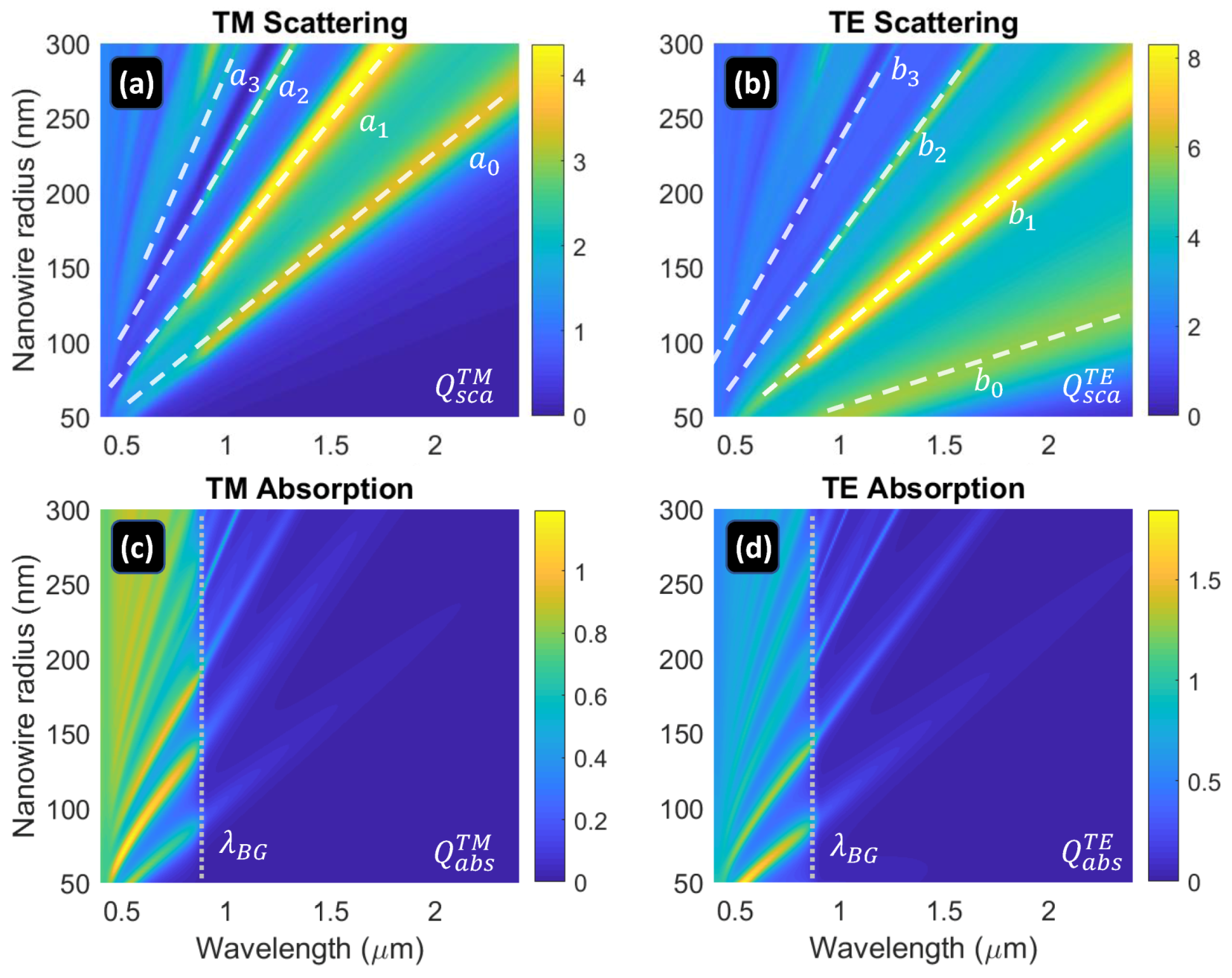
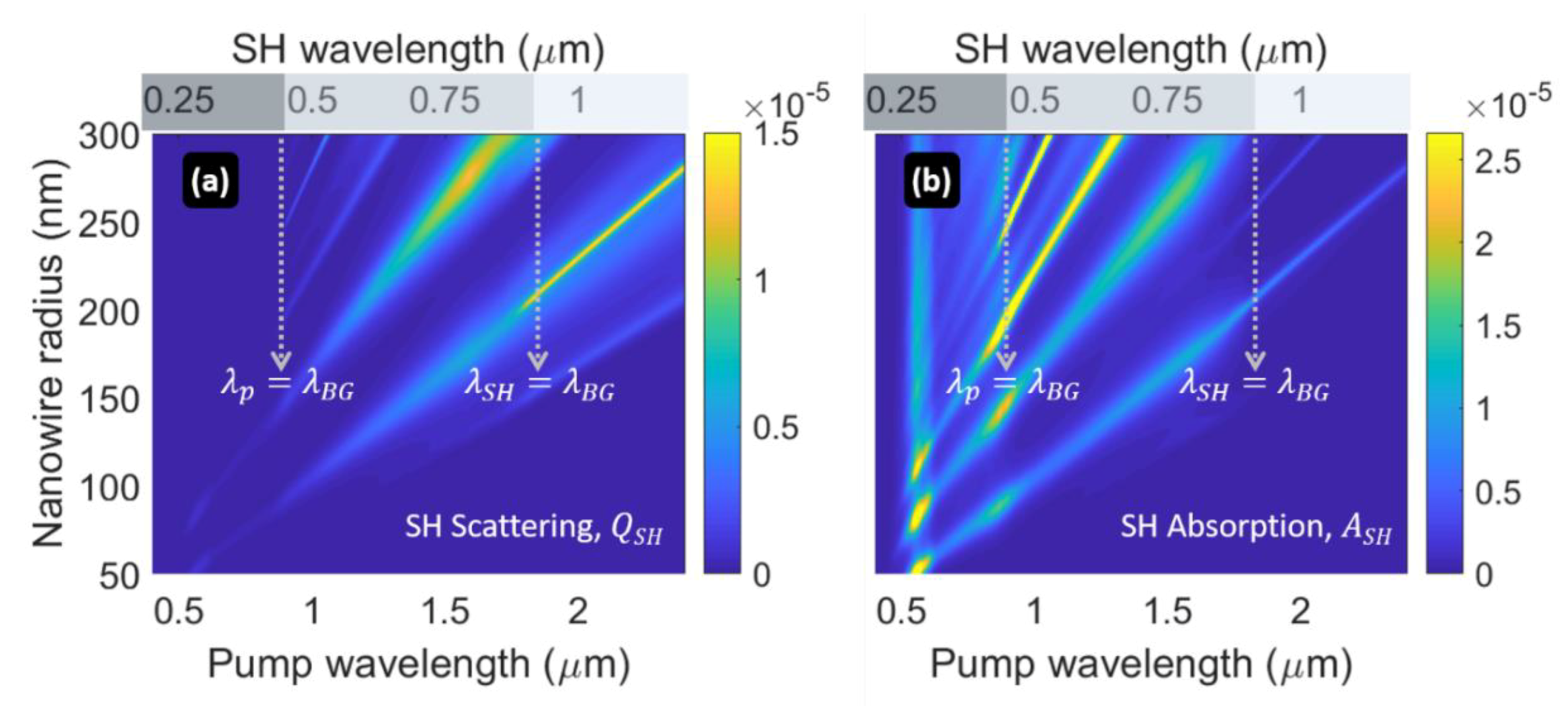
Maps of scattering and absorption efficiency spectra for plane wave excitation are reported in Figure 2 as a function of the nanowire radius. The efficiencies are calculated in the linear regime, i.e., assuming the input light intensity induces negligible nonlinear polarization sources in GaAs. Under these circumstances the problem can be approached by using Mie theory and the scattering and absorption efficiencies can be evaluated as normalized cross-sections. The normalization factor is the power (per unit length) flowing through the geometric cross-section, 2 r N W I i n c , where r N W is the nanowire radius and I i n c is the input light intensity [27]. In other words, scattering efficiencies, Q s c a T E , T M , and absorption cross sections, Q a b s T E , T M , are evaluated, for TE- and TM-polarized incident plane waves, as follows:
Q s c a T E = 2 x ( | b 0 | 2 + 2 1 | b n | 2 )
Q s c a T M = 2 x ( | a 0 | 2 + 2 1 | a n | 2 )
Q a b s T E = 2 x Re ( b 0 + 2 1 b n ) 2 x ( | b 0 | 2 + 2 1 | b n | 2 )
Q a b s T M = 2 x Re ( a 0 + 2 1 a n ) 2 x ( | a 0 | 2 + 2 1 | a n | 2 )
where x = k r N W and k is the wavenumber in the background medium. In our simple geometry, with a cylindrical nanowire, the scattering coefficients for TE-polarized light scattering, i.e., b n , and TM-polarized light scattering, i.e., a n , retrieved by imposing continuity of the tangential fields at the nanowire surface, are written as follows [27]:
a n = m J n ( x ) J n ( m x ) J n ( m x ) J n ( x ) m H n ( x ) J n ( m x ) J n ( m x ) H n ( x ) ,
b n = J n ( x ) J n ( m x ) m J n ( m x ) J n ( x ) H n ( x ) J n ( m x ) m J n ( m x ) H n ( x ) ,
where m = ϵ G a A s ϵ b is the nanowire index contrast, J n are the Bessel functions of first kind and order n and J n their derivatives, whereas H n are the Hankel functions of first kind and H n their derivatives.
It is worth mentioning that TE and TM problems are fully decoupled in our z -invariant structure with scattering only occurring in the x y -plane. Incident, scattered and internal fields are superpositions of vector cylindrical harmonics, namely superpositions of Hankel or Bessel functions. These harmonics are the normal modes of the particle. In particular, for an incident TM-polarized plane wave with electric-field amplitude E i n c , the scattered field outside the nanowire ( r > r N W ) can be written as follows:
E S T M ( r , ϕ ) = E i n c n = ( i ) n i a n [ i n k r H n ( k r ) ρ ^ H n ( k r ) ϕ ^ ] e i n ϕ ,
H S T M ( r , ϕ ) = i E i n c η n = ( i ) n i a n H n ( k r ) z ^ e i n ϕ ,
where η = η 0 / ϵ b is the impedance of the background medium and η 0 the impedance in vacuo, and r ^ ϕ ^ z ^ are the unit vectors of a cylindrical coordinate system in which the axial coordinate, z , is aligned with the nanowire axis. By duality, for a TE-polarized plane wave the scattered field outside the nanowire is as follows:
E S T E ( r , ϕ ) = E i n c n = ( i ) n b n H n ( k r ) z ^ e i n ϕ
H S T E ( r , ϕ ) = i E i n c η n = ( i ) n b n [ i n k r H n ( k r ) r ^ H n ( k r ) ϕ ^ ] e i n ϕ .
The vector cylindrical harmonics inside the nanowire can be evaluated by substitution of H n ( k r ) and H n ( k r ) with J n ( m k r ) and J n ( m k r ) , respectively. For example, the TM and TE-polarized electric fields inside the nanowire can be calculated as follows:
E 1 T M ( r , ϕ ) = E i n c n = ( i ) n i d n [ i n m k r J n ( m k r ) ρ ^ + J n ( m k r ) ϕ ^ ] e i n ϕ
E 1 T E ( r , ϕ ) = E i n c n = ( i ) n c n J n ( m k r ) z ^ e i n ϕ ,
with internal scattering coefficients:
d n = 2 i / π x m H n ( x ) J n ( m x ) J n ( m x ) H n ( x ) ,
c n = 2 i / π x H n ( x ) J n ( m x ) m J n ( m x ) H n ( x ) .
It is clear that electric (magnetic) fields in TM polarization have the same shape and symmetry of magnetic (electric) fields in TE polarization, with the only difference being the scattering coefficients. Figure 2 summarizes this concept.
TE light scattering only depends on the b n   ( c n inside the nanowire) coefficients, while TM scattering is only ruled by the a n   ( d n inside the nanowire) coefficients. Although the expansions in Equations (2)–(5) are valid for plane waves, it is possible to expand the fields with the same Mie coefficients in the presence of any kind of source, including SH sources induced in the volume and on the surface of the nanowire. In other words, TE(TM) scattered fields are always equal to the superposition of normal modes of an increasing order number, each weighted by the corresponding coefficient b n   ( a n ). The normal modes of an open cavity must radiate into the far-field [28], and therefore it is common to associate them with cartesian multipoles [29,30]. For example, the Mie coefficient a 0 is related to a magnetic-dipole moment (or electric quadrupole [29,31]) and the associated electric field is of type a 0 H 0 ( k r ) ϕ ^ ; the coefficient a 1 is associated with a superposition of an electric dipole moment and a combination of electric-octupole moments. Higher-order coefficients a n , with n > 1 , are related to higher-order multipoles. TE-polarized normal modes are instead weighted by the b n coefficient and they are z-polarized. The coefficient b 0 is related to a TE mode with electric field distribution associated with an electric dipole, therefore of type a 0 H 0 ( r ) z ^ . Similarly, in the TM case, coefficients b n with n 1 are associated with higher-order modes. In Figure 2, we summarize the electric and magnetic field distributions associated with the first four TE- and TM-polarized modes with the corresponding Mie coefficients.
In Figure 3, we report scattering and absorption linear efficiencies, calculated with Equations (2)–(5), in response to either TE or TM polarized plane waves impinging on the nanowire. The scattering peaks are associated with the maxima of the Mie scattering coefficients, therefore, they correspond to maxima of either a n for the TM case or b n for the TE case—the maxima occur when the denominators of the scattering coefficients, d n and a n for TM polarization and c n and b n for TE polarization approach zero. The Mie coefficients peaks overlapped with the scattering and absorption maxima are reported in Figure 3. On each maximum of a Mie coefficient, light is efficiently coupled to the corresponding normal mode and intensity maxima of internal near-fields and scattered far-fields are observable. For this reason, maxima of scattering and absorption are virtually overlapped. The abrupt increase of absorption cross-section above the bandgap ( λ < λ B G ) is due to the electronic transitions of GaAs. Although quenched by absorption, resonances associated with higher-order modes appear at shorter wavelengths within the visible range. It is worth noticing that the response of the nanowire is dominated by four normal modes, namely the order 0 ,   ± 1 ,   ± 2 , and ± 3 , across the whole range of nanowire radii considered, from 50 to 300 nm, and across a broad wavelength range that covers visible and near-infrared.

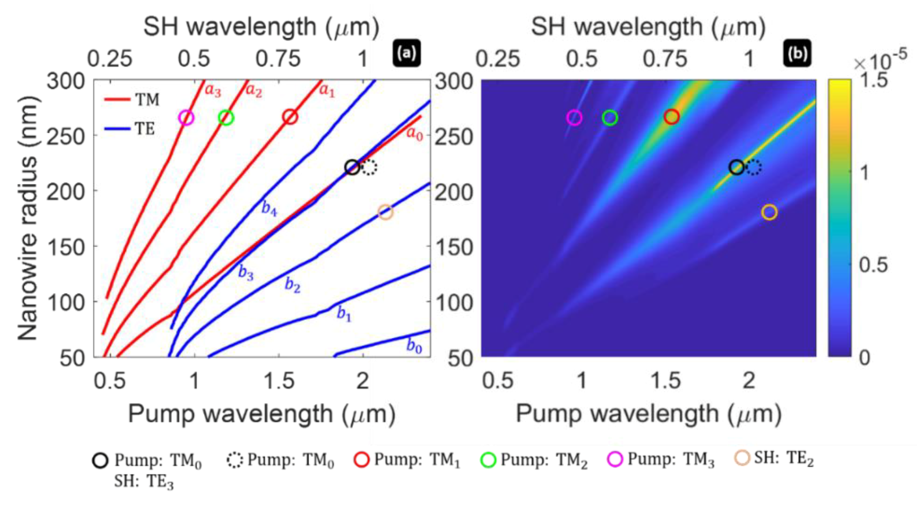
3. Second-Harmonic Generation: Scattering and Absorption Efficiencies

We consider an input pump with TM polarization and intensity I p = 2   GW / cm 2 . The second-order bulk response due to χ x y z ( 2 ) will induce a TE-polarized SH signal. The normal modes available in the spectrum play a key role in determining the far-field emission efficiency and radiation pattern for SH light. We have investigated far-field SH radiation by varying the pump wavelength across the whole spectrum shown in Figure 3. The total SH scattered efficiency is calculated in two ways: (i) By introducing an effective nonlinear susceptibility retrieved from the linear response at both the pump and SH wavelengths; (ii) with a finite-element solver (COMSOL). The SH scattering efficiency is defined as
Q S H = C S S H n ^ d 2 r N W I p ,
where S S H is the Poynting vector at the SH wavelength in the far-field zone, and the integral is performed along a closed line surrounding the nanowire in the far-field with n ^ being the unit vector normal to the line and pointing in the outward direction. Neglecting pump depletion and third-order nonlinear effects, it is straightforward to prove that the SH scattering efficiency shows the usual linear dependence on the pump intensity I p and a simple dependence on an average nonlinear susceptibility, χ a v ( 2 ) , as follows:
Q S H = η b 4 ϵ b 2 π 2 ( k S H r N W ) 3 | χ a v ( 2 ) | 2 I p
where η b is the background impedance, k S H = 2 k = 2 ω p c ϵ b is the SH wavenumber in the background medium and the average susceptibility is calculated as the average of | χ e f f ( 2 ) ( ϕ ) | 2 , across all the possible SH scattering angles between 0 and 2 π in the xy plane, i.e.,
| χ a v ( 2 ) | 2 = | χ e f f ( 2 ) ( ϕ ) | 2 = 0 2 π | χ e f f ( 2 ) ( ϕ ) | 2 d ϕ 2 π .
The derivation of Equation (17) is based on the Lorentz reciprocity theorem, and it is reported in the Appendix A section. The angle-dependent, effective nonlinear coefficient, χ e f f ( 2 ) ( ϕ ) , is related to the field enhancement at both pump and SH and to the overlap integral in the volume of the nanowire ( N W ):
χ e f f ( 2 ) ( ϕ ) = N W χ x y z ( 2 ) ξ x ξ y ξ z ( ϕ ) d S π r N W 2 .
In Equation (19), ξ x is the E x field distribution in the nanowire under TM plane wave excitation at the pump frequency with amplitude E i n c = 1   V / m and incident at φ = 0 , ξ y is the E y field distribution at the pump frequency under TM plane wave excitation with amplitude E i n c = 1   V / m and incident at φ = 0 , and ξ z ( ϕ ) is the E z field under TE plane wave excitation at the SH frequency with amplitude E i n c = 1   V / m and incident at φ = ϕ . The fields in Equation (19) are calculated in the linear regime and therefore they are evaluated by using the Mie-theory expressions presented in Equations (12)–(13). We have verified that truncating the cylindrical expansion of the fields in order to include only four normal modes in Equation (19) is enough to predict with good accuracy the SH scattering efficiency using the expression in Equation (17). The differences in the calculated Q S H values with respect to the finite-element numerical simulations (COMSOL) are on the order of 1%, and they are mainly due to the order of truncation of cylindrical harmonics in the fields’ expansions. The maxima of scattering coefficients are plotted in Figure 4 for a large range of nanowire radii next to the SH generation efficiency Q S H map.
It is clear that the peaks in the SH scattering spectrum are associated with the excitation of nanowire modes at the pump or at the SH wavelengths, or at both wavelengths if the system is doubly-resonant. In 
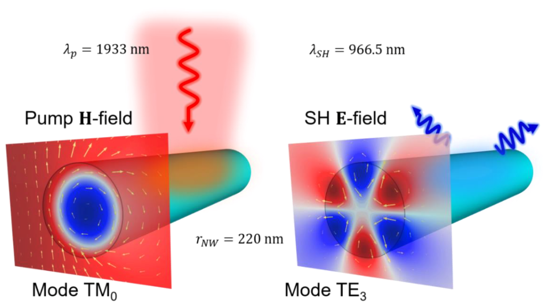
Figure 4, we have indicated with circles several SH peaks. In one case—see the black circle—the radius is equal to 220 nm and the pump wavelength is equal to ~1933 nm, therefore the SH is generated at 966.5 nm, in the transparency region of GaAs ( λ > λ B G ). In this scenario, the nanowire is doubly resonant for both the pump and the SH field, and this condition only occurs in a very narrow band. In particular, the pump plane wave is exciting the TM0 mode, which is related to a broadband peak of the Mie coefficient a 0 , whereas the SH is resonant with the mode TE3, which is associated with a narrowband peak of the Mie coefficient b 3 . The result of this doubly-resonant, TM 0 + TM 0 TE 3 interaction is that SH light is scattered with high efficiency, larger than 10 5 . In 
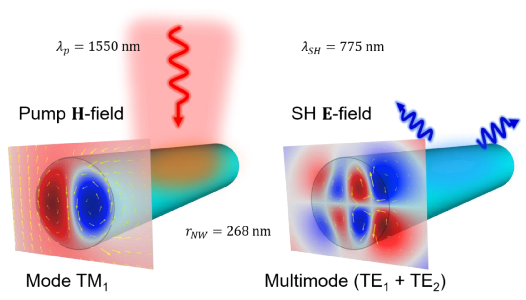
Figure 5, we plot the field distribution of the pump and SH on this peak, when the nanowire radius is r N W = 220   nm .
If the pump is slightly detuned from this double resonance condition, then the structure turns out to be singly-resonant with the only TM0 mode resonantly excited by the pump and a 4-fold reduction of conversion efficiency—the dotted black circle belongs to this singly-resonant region. This explains the spectral behavior of the SH efficiency near this region, with a sharp peak (due to SH coupling to the TE3 mode) emerging from a shallow peak (due to pump coupling to the TM0 mode). Owing to a combination of factors, including the chromatic dispersion of GaAs as well as the dispersion of the scattering coefficients, the double resonance condition persists over a wide range of nanowire sizes, form radii smaller than 200 nm to radii larger than 300 nm. Other peaks, indicated in Figure 4 with circles of different colors, are due to mode coupling of either the pump or SH to normal modes of the nanowire. It is remarkable that the conversion efficiency remains at similar levels, between 10−6 and 10−5, even in cases in which the SH wavelength, λ S H , is smaller than λ B G and therefore absorption losses are expected to inhibit up-conversion. In particular, on the peak indicated with a red circle—corresponding to a nanowire with radius 268 nm and pumped at 1550 nm—the efficiency is as high as in the doubly resonant case, even though only the pump signal is here resonantly coupled to the TM1 mode and the SH is tuned above the bandgap ( λ S H < λ B G ). The field distributions for pump and SH in this scenario are reported in Figure 6. While the pump takes on the typical shape of a TM1 mode, the SH is coupled to a superposition of modes, with the stronger components being the TE1 and the TE2, i.e., the modes associated with the b 1 an b 2 Mie coefficients, respectively.

4. Absorption of SH Light

The usual metrics for SH conversion efficiency involves the SH light that one may collect in a certain direction in the far-field region, or the total light scattered Q S H in all directions in the far-field, as defined in Equation (16). However, a portion of SH energy is inexorably dissipated in the near field via one-photon absorption. The rate of this SH absorption can be calculated as follows:
A S H = ω ϵ 0 / 2 2 r N W I i n c Im ( ϵ G a A s ) N W | E 1 T E | 2 d S ,
  A S H can be significant in enhanced nonlinear interactions at the nanoscale. For example, in plasmonic resonators, in addition to the pump energy lost as heat in the metal, reabsorption of SH light is orders of magnitude larger than far-field scattered SH light [32,33,34]. In other words, A S H > > Q S H in many nanoplasmonic systems designed to resonate at the pump and/or at the harmonic frequency. Dielectric resonators are considered immune to pump absorption if illuminated in the transparency region below the bandgap (i.e., if the pump wavelength λ P is larger than λ B G ), although Mie theory predicts that light absorption on the Mie resonances above the bandgap can reach values as high as 5% of the total light extinction for GaAs nanowires, as one can infer by comparing absorption maps and scattering maps in Figure 3. In addition, a study of SH light absorption in dielectric nanoantennas (isolated or in metasurfaces) has not been reported so far, taking for granted that most of the SH light is scattered in the far-field by dielectric resonators, and not absorbed in the near field. Here we demonstrate that this is not the case, at least for nanowires with 2D light-confinement. In Figure 7, we report a side-by-side comparison of SH scattering efficiency spectra, Q S H , and SH absorption spectra, A S H , as functions of the nanowire radii.
SH scattering peaks are associated with SH absorption peaks, as in other resonant photonic structure, including plasmonic nanoantennas and gratings. A S H is non-negligible with respect to Q S H . Indeed,   A S H is on the same order or even larger than Q S H for most resonant peaks, including those peaks that entirely fall in the transparency region of GaAs ( λ S H λ B G ). These facts are summarized in 
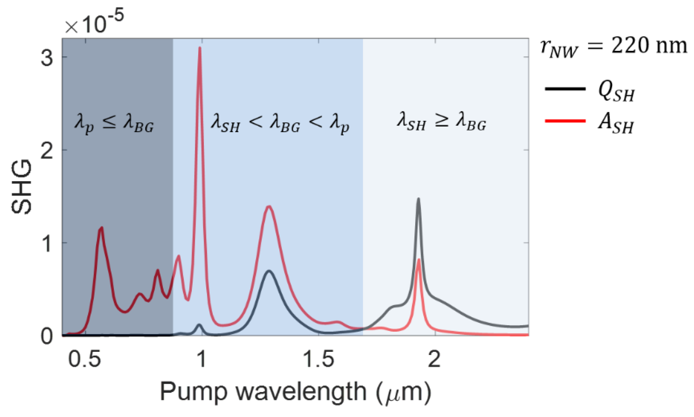
Figure 8, where the SH scattering and absorption spectra are plotted for a nanowire radius r N W = 220   nm illuminated with a TM polarized pump plane wave with intensity I p = 2   GW / cm 2 . In the transparent region ( λ S H λ B G ), in which GaAs is a poor absorber at both pump and SH wavelengths, scattering and absorption of SH light show similar efficiencies on the order of 10 5 on the doubly-resonant peak at λ p 1.933   μ m . In the intermediate wavelength range in which GaAs is mostly transparent for the pump but absorbing for the SH ( λ S H < λ B G < λ p ), SH absorption gets somewhat larger than SH scattering but the scattering efficiency reaches almost the same level that one has in the fully transparent region (see, e.g., the peak at λ p 1.29   μ m ). In the opaque range ( λ p λ B G ), SH absorption dominates over scattering by at least one order of magnitude.

5. Conclusions

To summarize, we have investigated SH generation from Mie-resonant GaAs nanowires. When judiciously designed, nanowires are able to boost the conversion efficiency of SH generation up to 10 5 using a ~ 1   GW / cm 2 pump intensity, similar to the efficiency previously reported in 3D confined dielectric antennas made of GaAs and AlGaAs. We have found a doubly-resonant condition in which both the pump and the SH fields excite normal modes of the nanowire, a scenario that can be achieved in a large range of pump wavelengths by changing the nanowire radius. When the nanowire is under doubly-resonant conditions, the SH light is coupled to a multipolar normal mode with large quality factor (the bandwidth of the SH scattering peak is as narrow as ~15 nm). Such narrow spectral features may be exploited for sensing devices, tunable filters, and modulators.
Our results suggest that, due to the resonant nature of SH generation in GaAs nanowires, on one hand, SH scattering in the opaque region of GaAs may be as efficient as in the transparency region, and, on the other hand, SH absorption in the transparency region may be as strong as in the opaque region of GaAs.

Author Contributions

Conceptualization, D.d.C., L.C., M.A.V., C.D.A., M.S.; methodology, D.d.C., L.C., M.A.V., C.D.A., M.S.; software, D.d.C., L.C.; validation, M.A.V., C.D.A., M.S.; formal analysis, D.d.C., L.C., M.A.V., C.D.A., M.S.; investigation, D.d.C., L.C., M.A.V., C.D.A., M.S.; resources, D.d.C., L.C., M.A.V., C.D.A., M.S.; data curation, D.d.C., L.C., M.A.V., C.D.A., M.S.; writing—original draft preparation, D.d.C.; writing—review and editing, L.C., M.A.V., C.D.A., M.S.; visualization, D.d.C., L.C., M.A.V., C.D.A., M.S.; supervision, D.d.C., C.D.A., M.S.; project administration, M.A.V., D.d.C., L.C.; funding acquisition, D.d.C., L.C., M.A.V., C.D.A., M.S.

Funding

This research was funded by the US Army Research Office, grant number W911NF-18-1-0424.

Acknowledgments

Research of M.A.V. was partially funded by the Rita Levi-Montalcini Program. L.C. acknowledges STARStG project PULSAR. Research of D.d.C. was sponsored by the RDECOM-Atlantic, US Army Research Office, and Office of Naval Research Global, and partly performed within Project “Internet of Things: Sviluppi Metodologici, Tecnologici E Applicativi”, cofunded (2018–2022) by the Italian Ministry of Education, Universities and Research (MIUR) under the aegis of the “Fondo per il finanziamento dei dipartimenti universitari di eccellenza” initiative (Law 232/2016). D.d.C. thanks Gianluca Marcon for fruitful discussions.

Conflicts of Interest

The authors declare no conflict of interest.

Appendix A

The expression of the SH scattering efficiency in Equation (17) derives from the Lorentz reciprocity theorem and the concept of effective susceptibility [35,36,37]. In the undepleted pump approximation and in the absence of third-order nonlinear effects, the time-harmonic electromagnetic problem at the SH frequency ( 2 ω p ) is given by a distribution of volume currents localized inside the nanowire,
J N L = i 2 ω p P N L = i 2 ω p ( ϵ 0 χ x y z ( 2 ) E 1 , x T M E 1 , y T M ) z ^ ,
which radiate into the background medium and induce the unknown field E S H ( R , ϕ ) = E S H z ^ at a distance R from the nanowire in a direction tilted by an angle ϕ with respect to the input pump, where a virtual detector is located. The problem is illustrated in Figure A1a. In Figure A1b, we also report the reciprocal problem, in which a line current source J 0 = I 0 δ ( x x 0 ) δ ( y y 0 ) z ^ , at the virtual-detector location, emits radiation of frequency 2 ω p and induces a z-polarized field E 1 T E = E 1 , z T E z ^ inside the nanowire. The Lorentz reciprocity imposes that
  J 0 E S H d S =   J N L E 1 T E d S
where the surface integral is performed across the whole x y plane. The expression of the unknown field is therefore:
E S H = i 2 ϵ 0 ω p I 0 N W χ x y z ( 2 ) E 1 , x T M E 1 , y T M E 1 , z T E ( ϕ ) d S .
If the source J 0 is located in the far-field region, then the phase fronts emitted by J 0 at the nanowire position are virtually planar. Under these circumstances, it is convenient to replace, in the reciprocal problem, the current J 0 with a z-polarized plane wave with amplitude E 0 and traveling in the direction ϕ , as illustrated in Figure A1c. This plane wave induces an electric field E 1 , z T E   ( ϕ ) identical to that produced in the original reciprocal problem of Figure A1b. The plane wave excitation may be more practical for full-wave numerical simulations. An additional advantage is that all the internal fields in the integral of Equation (A3) can now be retrieved analytically by using the expressions in Equations (12)–(13).
Figure A1. (a) SH scattering problem, with a volume current distribution J N L inside the nanowire radiating into the background medium and inducing a field E S H on a detector located in a point in the far-field. (b) Reciprocal scattering problem, with a radiating line current source located at the detector point that induces a field E 1 T E inside the nanowire. (c) The equivalent of (b) with a plane wave source instead of a line current (the approximation is valid if k S H R 1 ).
Applsci 09 03381 g0a1
The only missing piece of information is the relation between the plane wave amplitude E 0 and the current I 0 . This can be retrieved by solving for the 2D Green’s function for the Helmholtz equation at the SH frequency in the plane of scattering ( x y plane), G 2 D = i 4 H 0 ( 1 ) ( k S H R ) . Using the asymptotic approximation of the Hankel function for k S H R 1 , the Green’s function reduces to:
G 2 D e i π 4 e i k S H R 8 π k S H R .
The vector potential for the current source J 0 is, at a distance R from J 0 :
A 0 = μ 0   J 0 G 2 D d S = μ 0 I 0 e i π 4 e i k S H R 8 π k S H R   z ^ .
The electric field associated with this vector potential is therefore:
E 0 = i 2 ω p A 0 = i 2 ω p μ 0 I 0 e i π 4 e i k S H R 8 π k S H R   z ^ .
Hence, the plane wave amplitude is
E 0 = | E 0 | = 2 ω p μ 0 I 0 8 π k S H R
and Equation (A3) can be re-written as follows:
E S H = i 4 μ 0 ϵ 0 ω p 2 8 π k S H R N W χ x y z ( 2 ) E 1 , x T M E 1 , y T M E 1 , z T E ( ϕ ) | E 0 | d S .
If we now consider a TM-polarized plane-wave field at the fundamental frequency ω p , with pump intensity I p = 1 2 ϵ 0 ϵ b c | E p | 2 , and indicate with ξ x / y = E 1 , x / y T M / | E p | the field enhancement profiles for the x and y component of the TM-polarized pump field, and ξ z ( ϕ ) = E 1 , z T E ( ϕ ) | E 0 | the analogous quantity for the z component of the TE-polarized SH field, then Equation (A8) can be recast as follows:
E S H = i 8 μ 0 I p ω p 2 c ϵ b 8 π k S H R π r N W 2 χ e f f ( 2 ) ( ϕ )
where
χ e f f ( 2 ) ( ϕ ) = N W χ x y z ( 2 ) ξ x ξ y ξ z ( ϕ ) d S π r N W 2
is the angle-dependent, effective nonlinear coefficient reported in Equation (19).
The Poynting vector can now be written as:
S S H = | E S H | 2 2 η b n ^ = η b I p 2 k S H 3 π r N W 4 4 R ϵ b 2 | χ e f f ( 2 ) ( ϕ ) | 2 n ^ ,
where η b is the background impedance.
Finally, the expression of the SH scattering efficiency reported in Equation (17) of the main text can be derived:
Q S H = C S S H n ^ d 2 r N W I p = η b 4 ϵ b 2 π 2 ( k S H r N W ) 3 | χ a v ( 2 ) | 2 I p ,
where the average susceptibility is defined as in Equation (18):
| χ a v ( 2 ) | 2 = | χ e f f ( 2 ) ( ϕ ) | 2 = 0 2 π | χ e f f ( 2 ) ( ϕ ) | 2 d ϕ 2 π .

References

  1. Boyd, R.W. Nonlinear Optics; Academic Press: Cambridge, MA, USA, 2003. [Google Scholar]
  2. Bloembergen, N.; Pershan, P.S. Light Waves at the Boundary of Nonlinear Media. Phys. Rev. 1962, 128, 606–622. [Google Scholar] [CrossRef] [Green Version]
  3. Scalora, M.; Bloemer, M.J.; Manka, A.S.; Dowling, J.P.; Bowden, C.M.; Viswanathan, R.; Haus, J.W. Pulsed second-harmonic generation in nonlinear, one-dimensional, periodic structures. Phys. Rev. A 1997, 56, 3166–3174. [Google Scholar] [CrossRef]
  4. De Angelis, C.; Gringoli, F.; Midrio, M.; Modotto, D.; Aitchison, J.S.; Nalesso, G.F. Conversion efficiency for second-harmonic generation in photonic crystals. J. Opt. Soc. Am. B 2001, 18, 348. [Google Scholar] [CrossRef]
  5. Dumeige, Y.; Vidakovic, P.; Sauvage, S.; Sagnes, I.; Levenson, J.A.; Sibilia, C.; Centini, M.; D’Aguanno, G.; Scalora, M. Enhancement of second-harmonic generation in a one-dimensional semiconductor photonic band gap. Appl. Phys. Lett. 2001, 78, 3021–3023. [Google Scholar] [CrossRef]
  6. D’Aguanno, G.; Centini, M.; Scalora, M.; Sibilia, C.; Dumeige, Y.; Vidakovic, P.; Levenson, J.A.; Bloemer, M.J.; Bowden, C.M.; Haus, J.W.; et al. Photonic band edge effects in finite structures and applications to χ(2) interactions. Phys. Rev. E 2001, 64, 016609. [Google Scholar] [CrossRef] [PubMed]
  7. Dumeige, Y.; Sagnes, I.; Monnier, P.; Vidakovic, P.; Abram, I.; Mériadec, C.; Levenson, A. Phase-Matched Frequency Doubling at Photonic Band Edges: Efficiency Scaling as the Fifth Power of the Length. Phys. Rev. Lett. 2002, 89, 043901. [Google Scholar] [CrossRef] [PubMed]
  8. Malvezzi, A.M.; Vecchi, G.; Patrini, M.; Guizzetti, G.; Andreani, L.C.; Romanato, F.; Businaro, L.; Di Fabrizio, E.; Passaseo, A.; De Vittorio, M. Resonant second-harmonic generation in a GaAs photonic crystal waveguide. Phys. Rev. B 2003, 68, 161306. [Google Scholar] [CrossRef] [Green Version]
  9. De Ceglia, D.; D’Aguanno, G.; Mattiucci, N.; Vincenti, M.; Scalora, M. Enhanced second-harmonic generation from resonant GaAs gratings. Opt. Lett. 2011, 36, 704–706. [Google Scholar] [CrossRef]
  10. Cowan, A.R.; Young, J.F. Mode matching for second-harmonic generation in photonic crystal waveguides. Phys. Rev. B 2002, 65, 085106. [Google Scholar] [CrossRef]
  11. Shcherbakov, M.R.; Neshev, D.N.; Hopkins, B.; Shorokhov, A.S.; Staude, I.; Melik-Gaykazyan, E.V.; Decker, M.; Ezhov, A.A.; Miroshnichenko, A.E.; Brener, I.; et al. Enhanced Third-Harmonic Generation in Silicon Nanoparticles Driven by Magnetic Response. Nano Lett. 2014, 14, 6488–6492. [Google Scholar] [CrossRef]
  12. Carletti, L.; Locatelli, A.; Stepanenko, O.; Leo, G.; De Angelis, C. Enhanced second-harmonic generation from magnetic resonance in AlGaAs nanoantennas. Opt. Express 2015, 23, 26544–26550. [Google Scholar] [CrossRef] [PubMed] [Green Version]
  13. Gili, V.F.; Carletti, L.; Locatelli, A.; Rocco, D.; Finazzi, M.; Ghirardini, L.; Favero, I.; Gomez, C.; Lemaitre, A.; Celebrano, M.; et al. Monolithic AlGaAs second-harmonic nanoantennas. Opt. Express 2016, 24, 15965–15971. [Google Scholar] [CrossRef] [PubMed] [Green Version]
  14. Saravi, S.; Keeler, G.A.; Sinclair, M.B.; Reno, J.; Pertsch, T.; Liu, S.; Brener, I.; Yang, Y. Resonantly enhanced second-harmonic generation using III-V semiconductor all-dielectric metasurfaces. Nano Lett. 2016, 16, 5426–5432. [Google Scholar]
  15. Liu, H.; Guo, C.; Vampa, G.; Zhang, J.L.; Sarmiento, T.; Xiao, M.; Bucksbaum, P.H.; Vučkovicć, J.; Fan, S.; Reis, D.A. Enhanced high-harmonic generation from an all-dielectric metasurface. Nat. Phys. 2018, 14, 1006. [Google Scholar] [CrossRef]
  16. Scalora, M.; Trull, J.; Cojocaru, C.; Vincenti, M.A.; Carletti, L.; de Ceglia, D.; Akozbek, N.; De Angelis, C. Resonant, broadband, and highly efficient optical frequency conversion in semiconductor nanowire gratings at visible and UV wavelengths. J. Opt. Soc. Am. B 2019, 36, 2346–2351. [Google Scholar] [CrossRef]
  17. Kuznetsov, A.I.; Miroshnichenko, A.; Brongersma, M.L.; Kivshar, Y.S.; Lukyanchuk, B. Optically resonant dielectric nanostructures. Science 2016, 354, aag2472. [Google Scholar] [CrossRef] [PubMed] [Green Version]
  18. Kauranen, M.; Zayats, A.V. Nonlinear plasmonics. Nat. Photonics 2012, 6, 737–748. [Google Scholar] [CrossRef]
  19. Carletti, L.; Koshelev, K.; De Angelis, C.; Kivshar, Y. Giant Nonlinear Response at the Nanoscale Driven by Bound States in the Continuum. Phys. Rev. Lett. 2018, 121, 033903. [Google Scholar] [CrossRef] [Green Version]
  20. Camacho-Morales, R.; Rahmani, M.; Kruk, S.; Wang, L.; Xu, L.; Smirnova, D.A.; Solntsev, A.S.; Miroshnichenko, A.; Tan, H.H.; Karouta, F.; et al. Nonlinear Generation of Vector Beams From AlGaAs Nanoantennas. Nano Lett. 2016, 16, 7191–7197. [Google Scholar] [CrossRef]
  21. Neshev, D.; Carletti, L.; Locatelli, A.; De Angelis, C. Shaping the Radiation Pattern of Second-Harmonic Generation from AlGaAs Dielectric Nanoantennas. ACS Photonics 2016, 3, 1500–1507. [Google Scholar]
  22. Smirnova, D.; Kivshar, Y.S. Multipolar nonlinear nanophotonics. Optica 2016, 3, 1241. [Google Scholar] [CrossRef]
  23. Rakić, A.D.; Majewski, M.L. Modeling the optical dielectric function of GaAs and AlAs: Extension of Adachi’s model. J. Appl. Phys. 1996, 80, 5909–5914. [Google Scholar] [CrossRef]
  24. Bethune, D.; Schmidt, A.J.; Shen, Y.R. Dispersion of nonlinear optical susceptibilities of InAs, InSb, and GaAs in the visible region. Phys. Rev. B 1975, 11, 3867–3875. [Google Scholar] [CrossRef] [Green Version]
  25. Bergfeld, S.; Daum, W. Second-Harmonic Generation in GaAs: Experiment versus Theoretical Predictions of chi(2)xyz. Phys. Rev. Lett. 2003, 90, 036801. [Google Scholar] [CrossRef] [PubMed]
  26. Trolle, M.L. Microscopic Theory of Linear & Nonlinear Optical Response: Zinc-Blende Semiconductors. Master’s Thesis, Aalborg University, Aalborg, Denmark, 2011. [Google Scholar]
  27. Bohren, C.F.; Huffman, D.R. Absorption and Scattering of Light by Small Particles; Wiley: Hoboken, NJ, USA, 1998. [Google Scholar]
  28. Richtmyer, R.D. Dielectric Resonators. J. Appl. Phys. 1939, 10, 391. [Google Scholar] [CrossRef]
  29. Grahn, P.; Shevchenko, A.; Kaivola, M. Electromagnetic multipole theory for optical nanomaterials. New J. Phys. 2012, 14, 93033. [Google Scholar] [CrossRef]
  30. Raab, R.E.; de Lange, O.L. Multipole Theory in Electromagnetism; Oxford University Press: New York, NY, USA, 2005. [Google Scholar]
  31. De Ceglia, D.; Vincenti, M.A.; De Angelis, C.; Locatelli, A.; Haus, J.W.; Scalora, M. Role of antenna modes and field enhancement in second harmonic generation from dipole nanoantennas. Opt. Express 2015, 23, 1715–1729. [Google Scholar] [CrossRef] [PubMed] [Green Version]
  32. Vincenti, M.A.; de Ceglia, D.; De Angelis, C.; Scalora, M. Surface-plasmon excitation of second-harmonic light: Emission and absorption. J. Opt. Soc. Am. B 2017, 34, 633. [Google Scholar] [CrossRef]
  33. De Ceglia, D.; Vincenti, M.A.; Akozbek, N.; Bloemer, M.J.; Scalora, M. Nested plasmonic resonances: Extraordinary enhancement of linear and nonlinear interactions. Opt. Express 2017, 25, 3980. [Google Scholar] [CrossRef]
  34. Vincenti, M.A.; Scalora, M.; de Ceglia, D. On the origin of third harmonic light from hybrid metal-dielectric nanoantennas. J. Opt. 2016, 18, 115002. [Google Scholar]
  35. Roke, S.; Bonn, M.; Petukhov, A.V. Nonlinear optical scattering: The concept of effective susceptibility. Phys. Rev. B 2004, 70, 115106. [Google Scholar] [CrossRef] [Green Version]
  36. Lee, J.; Tymchenko, M.; Argyropoulos, C.; Chen, P.-Y.; Lu, F.; Demmerle, F.; Boehm, G.; Amann, M.-C.; Alù, A.; Belkin, M.A. Giant nonlinear response from plasmonic metasurfaces coupled to intersubband transitions. Nature 2014, 511, 65–69. [Google Scholar] [CrossRef] [PubMed]
  37. O’Brien, K.; Suchowski, H.; Rho, J.; Salandrino, A.; Kante, B.; Yin, X.; Zhang, X. Predicting nonlinear properties of metamaterials from the linear response. Nat. Mater. 2015, 14, 379–383. [Google Scholar] [CrossRef] [PubMed]
Figure 1. (a) Real and imaginary parts of the GaAs relative permittivity, ϵ G a A s , in the wavelength range of interest. (b) Real and imaginary parts, and amplitude, of the GaAs second-order nonlinear susceptibility, χ ( 2 ) for second-harmonic (SH) generation. The x -axis in (b) refers to pump wavelength.
Applsci 09 03381 g001
Figure 2. Field distribution in the scattering plane ( x y ) associated with the first four normal modes with TE and TM polarization.
Applsci 09 03381 g002
Figure 3. Scattering (a,b) and absorption (c,d) efficiency spectra for TE-polarized incident light (a,c) and TM-polarized incident light (b,d) for GaAs nanowires with variable radius, r N W . The white dashed lines in (a,b) follow the maxima of the scattering coefficients. The white dotted lines indicate the electronic-bandgap wavelength of GaAs (~870 nm).
Applsci 09 03381 g003
Figure 4. (a) Maximum peaks of the Mie scattering coefficients monitored as a function of nanowire radius. For TM-scattering coefficients ( a n ), the wavelength axis is on the bottom (pump wavelength); for TE-scattering coefficients ( b n ), the wavelength axis in on the top (SH wavelength). (b) Color map representation of SH scattering efficiency as a function of wavelength and nanowire size. The circles in (a,b) highlight scenarios in which either the pump or the SH, or both pump and SH, are coupled to normal modes of the nanowire.
Applsci 09 03381 g004
Figure 5. Pump and SH field distribution for a GaAs nanowire with radius 220 nm illuminated with TM-polarized pump source tuned at 1933 nm.
Applsci 09 03381 g005
Figure 6. Pump and SH field distribution for a GaAs nanowire with radius 268 nm illuminated with TM-polarized pump source tuned at 1550 nm.
Applsci 09 03381 g006
Figure 7. (a) Same as Figure 4b. (b) SH absorption A S H , as a function of pump/SH wavelength and nanowire size. The dark-shaded portion of the SH wavelength axis indicates the opaque region for both pump and SH light ( λ p λ B G ); the medium-shaded portion indicates a region that is transparent for the pump but absorptive for the SH ( λ S H < λ B G < λ p ); the light-shaded portion indicates the transparent range ( λ S H λ B G ).
Applsci 09 03381 g007
Figure 8. SH scattering and absorption efficiency for a GaAs nanowire with r N W = 220   nm with an input pump intensity I p = 2   GW / cm 2 . The three background colors indicate the three regions described in the text with the same color code of Figure 7.
Applsci 09 03381 g008

