Article

Extension of an FFT-Based Beam Propagation Method to Plasmonic and Dielectric Waveguide Discontinuities and Junctions

1
Department of Electrical Engineering, Southern Taiwan University of Science and Technology, Tainan 71005, Taiwan
2
Department of Radiation Engineering, National Center for Radiation Research (NCRRT), Atomic Energy Authority, Cairo 11765, Egypt
3
Faculty of Engineering at Shobra, Banha University, Cairo 11672, Egypt
*
Author to whom correspondence should be addressed.
Appl. Sci. 2019, 9(20), 4362; https://doi.org/10.3390/app9204362
Submission received: 7 September 2019 / Revised: 7 October 2019 / Accepted: 11 October 2019 / Published: 16 October 2019
(This article belongs to the Special Issue Recent Advances in Plasmonics and Nanophotonics)

Abstract

:
We adapted a fast Fourier transform-based Beam Propagation Method (FFT-BPM) to investigate waveguide discontinuities in plasmonic waveguides. The adaptation of the FFT-BPM to treat transverse magnetic (TM) fields requires the circumvention of two major difficulties: the mixed derivatives of the magnetic field and waveguide refractive index profile in the TM wave equation and the step-like index change at the transverse metal-dielectric boundary of the plasmonic guide and the transverse boundaries of the dielectric waveguide as well. An equivalent-index method is adopted to transform TM fields to transverse electric (TE) ones, thus enabling the benefit of the full power and simplicity of the FFT-BPM. Moreover, an appropriate smoothing function is used to approximate the step-like refractive index profile in the transverse direction. At the junction plane, we used an accurate combined spatial-spectral reflection operator to calculate the reflected field. To validate our proposed scheme, we investigated the modal propagation in a silicon waveguide terminated by air (like a laser facet in two cases: with and without a coating layer). Then we considered a subwavelength plasmonic waveguide (metal-insulator-metal MIM) butt-coupled with a dielectric waveguide, where the power transmission efficiency has been calculated and compared with other numerical methods. The comparison reveals good agreement.

1. Introduction

Active and passive plasmonic devices are becoming one of the most promising candidates that could overcome the size mismatch between micro scale photonic devices and nanoscale electronic devices [1,2]. A promising way to achieve electrical control of light could be through plasmon polaritons—Coupled excitations of photons and electrons. Merging nanoelectronics and nano-optics enables the development of active subwavelength scale optics and an abundance of nano-optoelectronic devices and functionalities, such as tunable metamaterials, nanoscale optical processing, and strongly enhanced light-matter interactions for quantum devices and biosensing applications [3].
Recently [4], ultrafast optical switching of infrared plasmon polaritons has been reported in high-mobility graphene. The rapid progress in graphene plasmonics is propelled by their electrical tunability, high field confinement, potentially long lifetimes of plasmons and the strong light-matter interactions in graphene. It is worthy to note that advanced near-field imaging methods allow the plasmon-polariton waves to be efficiently launched and visualized as they travel along van der Waals materials layers (like graphene) or through multilayered heterostructures. This leads to strong nonlinearities, large photonic forces, and enhanced emission and absorption probabilities. A practical approach toward nanoscale light trapping and manipulation is offered by interfaces separating media with permittivities of opposite signs [5]. Graphene plasmons are very promising to be the best alternative to noble-metal plasmons as they exhibit much tighter confinement and relatively long propagation distances, with the advantage of being highly tunable via electrostatic gating [6].
The integration of plasmonic-based devices and photonic devices will eventually lead to an interfacing between plasmomic and photonic guides. Especially, butt-coupling plasmonic and dielectric guides is one of the most efficient ways for light transmission between highly confined modes and low-loss guided wave structures [7]. It is worthy to note that subwavelength optical confinement modes, allows the efficient and beneficial use of compact photonic devices like nanoscale photodetectors; thus, improving noise immunity, response speed and power dissipation in optical communication devices [8,9].
The versatility of the FFT-BPM in the simulation of wide range of photonic devices is well understood [10,11,12,13,14]. In this paper, for the sake of simplicity, we shall consider two-dimensional structures invariant in the y-direction. The main essence of the BPM is simple: propagation in a reference homogenous medium over a small distance Δz followed by phase correction that takes into account the spatial dependence of the refractive index of the medium. However, three major problems should be considered carefully when dealing with step discontinuity and plasmonic devices: The transverse magnetic nature of modes, the abrupt index change in the transverse direction and in the propagation direction at the junction plane [15].
Two remedies are used to circumvent the first two problems: the TM nature of the propagated mode is transformed to an equivalent TE field propagating in an equivalent refractive index medium [16,17]. Concerning the step-like transverse variation of the refractive index of the dielectric and plasmonic guides, we used a sigmoid-like function to approximate such abrupt index changes. It is worthy to note that many smoothing functions could be used [10,13,16]. We adopted the sigmoid function because of its simplicity in the analytical and numerical evaluation of the second derivative of the inverse index profile in the TM wave equation.
The third problem concerning the reflected field at the junction plane, we adopted a well-established, combined spatial-spectral operator formalism [12,14].
In this paper, a dielectric waveguide with its end facet terminated by air is considered in two cases: with and without coating layer. The power transmission at an abrupt plasmonic-dielectric waveguide junction is considered also and our results fairly agree with other accurate methods. Thus, demonstrating the adaptability of the FFT-BPM to treat such complex problems. We claim that the method presented in this paper could be extended to other types of interesting waveguide couplers, like the evanescent coupling between MIM-dielectric and MIM-MIM waveguides. Such coupling could be useful and efficient for nanoscale wavelength filters and ultra-fast optical switching as well as optical sensing application.

2. Reconsideration of TM Fields Difficulties:

The wave equation formalism in TE case can be written as:
[ 2 + k o 2 n 2 ( x ) ] E y ( x , z ) = 0
However, in TM case with z-invariant refractive index the wave equation for Hy (x, z) in a y-invariant structure takes the form [17]:
[ 2 + k o 2 n 2 1 n 2 n 2 x x ] H y ( x , z ) = 0
Where: ko = 2π/λo is the free space wavenumber and λo being the free-space wavelength. In a y-invariant structure 2 = ( 2 / x 2 + 2 / z 2 ) and n(x) is the refractive index profile of the planar waveguide with core refractive index nco surrounded by a cladding with index ncl. As stated earlier, the first problem facing the applicability of the FFT-based BPM in the solution of Equation (2) is the term involving the mixed derivative of the field and the inverse of the refractive index profile. Poladian et al. [17] suggested a transformation of the TM problem to a TE one via the following transformation:
H y ( x , z ) = n ( x ) F ( x , z )
Direct substitution of Equation (3) in Equation (2) results in the following wave equation for F(x, z):
2 F + k o 2 [ n 2 ( x ) n ( x ) k o 2 2 x 2 ( 1 n ( x ) ) ] F = 0
This can be written as:
[ 2 + k o 2 n e q 2 ( x ) ] F = 0
It is easy to conclude that Equation (5) is a TE problem with an equivalent index medium:
n e q 2 ( x ) = n 2 ( x ) n ( x ) k o 2 2 x 2 ( 1 n ( x ) )
The equivalent problem Equation (5) is amenable -in principle- to be solved via an FFT-based BPM algorithm. However, the step-like index profile n(x) is the second major problem that should be handled carefully. A judicious solution is to approximate n(x) by a suitable “smooth” function to circumvent the singularity in the transverse derivative x 2 ( 1 / n ( x ) ) in the equivalent index Equation (6). Accordingly, we adopted a sigmoid-like function nsig that approximates n(x) as follows:
n s i g ( x ) = n c l Δ n 1 + e a ( x h / 2 ) + Δ n 1 + e a ( x + h / 2 )
where ncl is the cladding refractive index, Δn is the difference between the waveguide cladding and core refractive indices, h is the waveguide core width, and a is the smoothing parameter that controls the steepness of the sigmoid function.
Each term f in the spatial-dependent part in Equation (7) has the important analytical property:
f 2 x 2 ( 1 f ) = 1 f
Thus n s i g x 2 ( 1 / n s i g ) is readily evaluated.
The extreme simplicity in the numerical evaluation of the above expression avoids the numerical artifacts and the generation of spurious modes that happen when evaluating numerically the second derivative as pointed out by [18].

3. Reconsideration of Reflected and Transmitted Fields:

The calculation of the reflected field Gr(x, 0) that is generated at the junction plane z = 0 between two waveguide is carried out using a combined spatial-spectral formalism in TE [12] and TM [14] cases as follows:
G r ( x , 0 ) = Δ r ( x , 0 ) 1 [ g i ( k x , 0 ) ρ ( k x , 0 ) ]
where gi (kx, 0) is the angular spectrum, i.e., the transverse (with respect to x) Fourier transform of the incident field Gi (x, 0) upon the junction plane, namely the guided mode of the incoming waveguide. This plane wave spectrum takes the form:
g i ( k x , 0 ) = G i ( x , 0 ) e j k x x d x
where, kx is the variable of the Fourier transform (the transverse wavenumber of the representative plane waves). The spectral part ρ(kx,0) is written as [14]:
ρ ( k x , 0 ) =   { k z k z + k z + k z + ( T E ) k z ( n 0 + ) 2 k z + ( n 0 ) 2 k z ( n 0 + ) 2 + k z + ( n 0 ) 2 ( T M )  
where, n 0 + and n 0 are certain reference refractive indices just immediately after and before the junction plane z = 0, as will be explained later. k z + and k z are the z-components of wave vectors of plane waves having transverse x-components kx in z > 0 and z < 0 respectively.
Namely,
k z = k 0 2 ( n o ) 2 k x 2
k z + = k 0 2 ( n o + ) 2 k x 2
The spatial dependent part of the reflection operator Δ r ( x , 0 ) in Equation (9) assumes the form:
Δ r ( x , 0 ) = r ( x , 0 ) r o
where:
r ( x , 0 ) =   { n ( x , 0 ) n ( x , 0 + ) n ( x , 0 + ) + n ( x , 0 ) ( T E ) n ( x , 0 + ) n ( x , 0 ) n ( x , 0 + ) + n ( x , 0 ) ( T M )  
and:
ro = r(xo,0)
where xo is the coordinate at which | r ( x , 0 ) | is maximum. Moreover, the reference refractive indices in Equation (11) are: n o + = n ( x o , 0 + ) and n o = n ( x o , 0 ) . Obviously, the refractive index distribution n ( x o , 0 ) is the index profile of the waveguide to the left of the junction, and n ( x o , 0 + ) is that one to the right of the junction. The transmitted field Ht (x, 0) across z = 0, follows directly from the boundary condition:
H t ( x , 0 ) = H i ( x , 0 ) + G r ( x , 0 )
where
H i = { E y i n   T E   c a s e H y i n   T M   c a s e

4. Numerical Results:

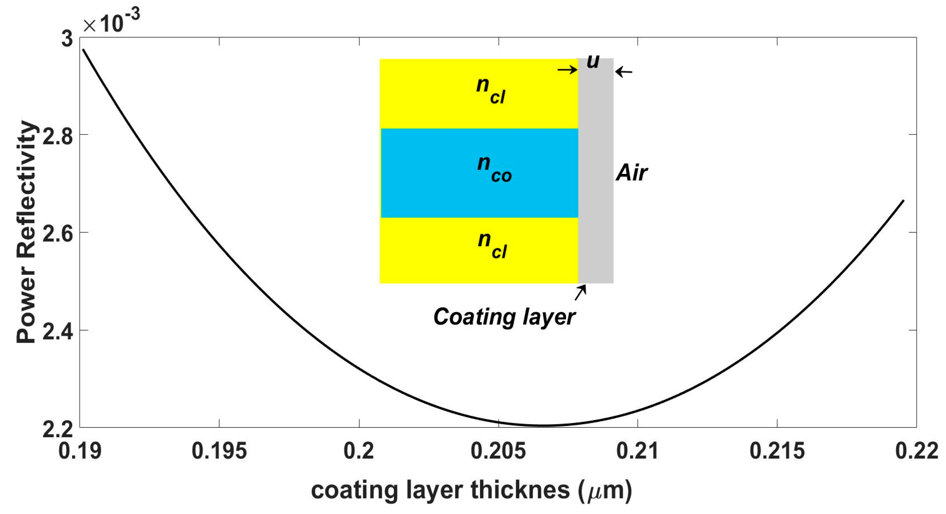
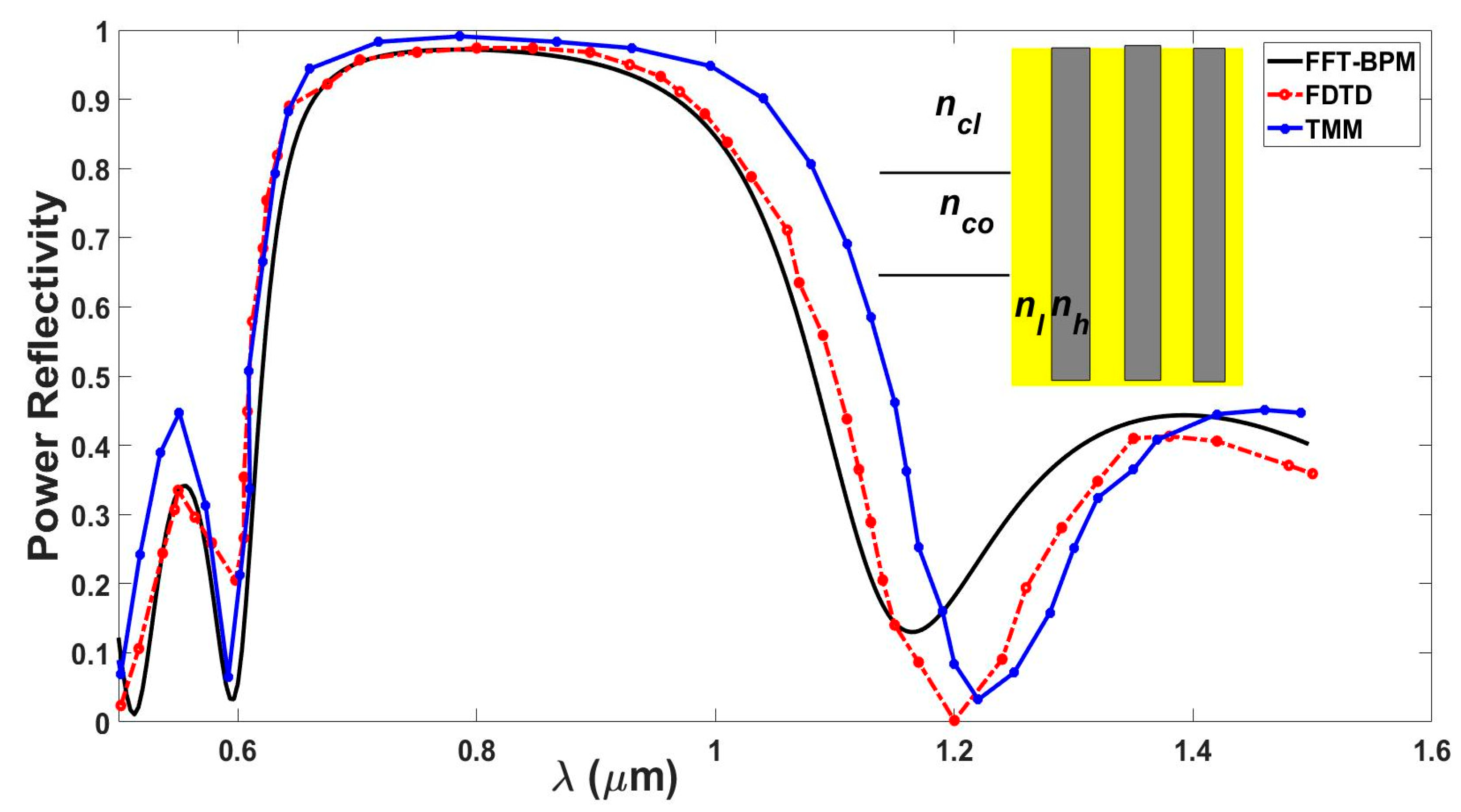
4.1. Dielectric Waveguide Facet

In fact, the waveguides terminated by air were studied using a variety of techniques [19,20,21,22,23,24,25] in TE and TM polarization modes. Figure 1 depicts the geometry of the problem under consideration (akin to waveguide Laser facet), where a three-layer dielectric slab waveguide occupying the half-space z < 0 is abruptly terminated by air at z = 0.
The waveguide core index is nco and width h, is surrounded by a cladding with refractive index ncl. An FFT-based BPM program including the reflection operator of Equation (9) has been implemented in Fortran to calculate the reflected power in TE and TM cases. The numerical values of the FFT-BPM algorithm are as follows: Number of sampling points along x-axis N = 216, sampling interval along the x-axis Δ x = 0.0003 λ o / n r e f , propagation step-size Δz = 1 nm. The dielectric waveguide core thickness h varies from 1 to 900 nm, the core refractive index is nco = 3.6, the cladding refractive index is expressed as a percentage δ of the core refractive index: n c l = n c o ( 1 δ ) (where δ = 3%, and 10%), and the free space wavelength λo = 0.86 µm. The fundamental TE and TM modal fields are calculated by solving numerically the corresponding eigenvalue equations [26]. Using the reflection operator formalism of the previous section, we calculated the reflected field at z = 0, and hence the transmitted field is readily evaluated via Equation (17). The power reflectivity is simply calculated as follows [24]:
P o w e r   reflectivity = ( | G r ( x ) H i * ( x ) d x | | H i ( x ) | 2 d x ) 2
Figure 2 compares the results of our method with those obtained by the accurate method of Vassallo [22] and the plane wave expansion (PWE) [24] at different values of δ = 3% and 10%, for both polarization TE (a) and TM (b). The curves of Figure 2 reveal a general good agreement.
The method is then applied to waveguides terminated by antireflection coating. A single layer coating is applied to a dielectric waveguide with nco = 3.6 and ncl = 3.564. The waveguide core width h is fixed at 1.457 µm. The coating layer has an index equal to the square root of the TE mode effective index ne, which is equal to 1.8938 at a wavelength λo = 1.55 µm. Figure 3 displays the power reflectivity as a function of the coating thickness u. Theoretically, the reflection from the coating layer is minimized when its thickness is equal to a quarter of the guided wavelength λg. So, we expect a minimum power reflectivity close to quarter the guided wavelength λg/4, where λg = λo/ne = 1.55/1.8938 = 0.8185 µm. Namely, the optimal coating layer thickness is expected to be close to 0.8185/4 = 0.205 µm. Figure 3 reveals a minimum reflectivity at u = 0.206 µm which agrees with λg/4 and with previously published results [23,24].
The extension to multiple dielectric layer is straightforward. Figure 4 shows the power reflectivity as function of the wavelength for high reflection coating with waveguide core width 0.487 µm.
The layers thickness is fixed to quarter wavelength. The core refractive index nco = 3.6, the cladding refractive index ncl = 3.24, and the high and low reflection coating material refractive indices are 3.5 and 1.7 respectively. Figure 4 exhibits a fair agreement with FDTD method and to a less degree with the Transfer Matrix Method (TMM) which fails to predict correctly the high reflectivity coating [24,25]. Yamautchi et al. [25] pointed out that the reflectivity calculated by the FDTD method deteriorates at long wavelengths (beyond 1 µm) due to the propagated field along the coating layers. This explains the disparity between the results of the FFT-BPM and the FDTD at long wavelengths.

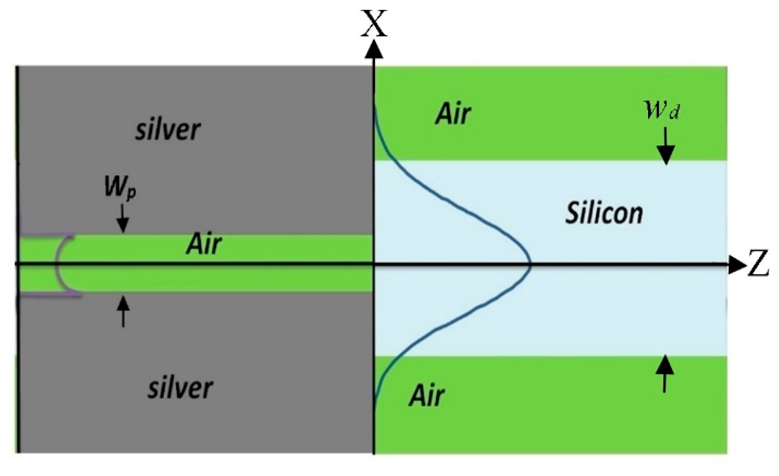
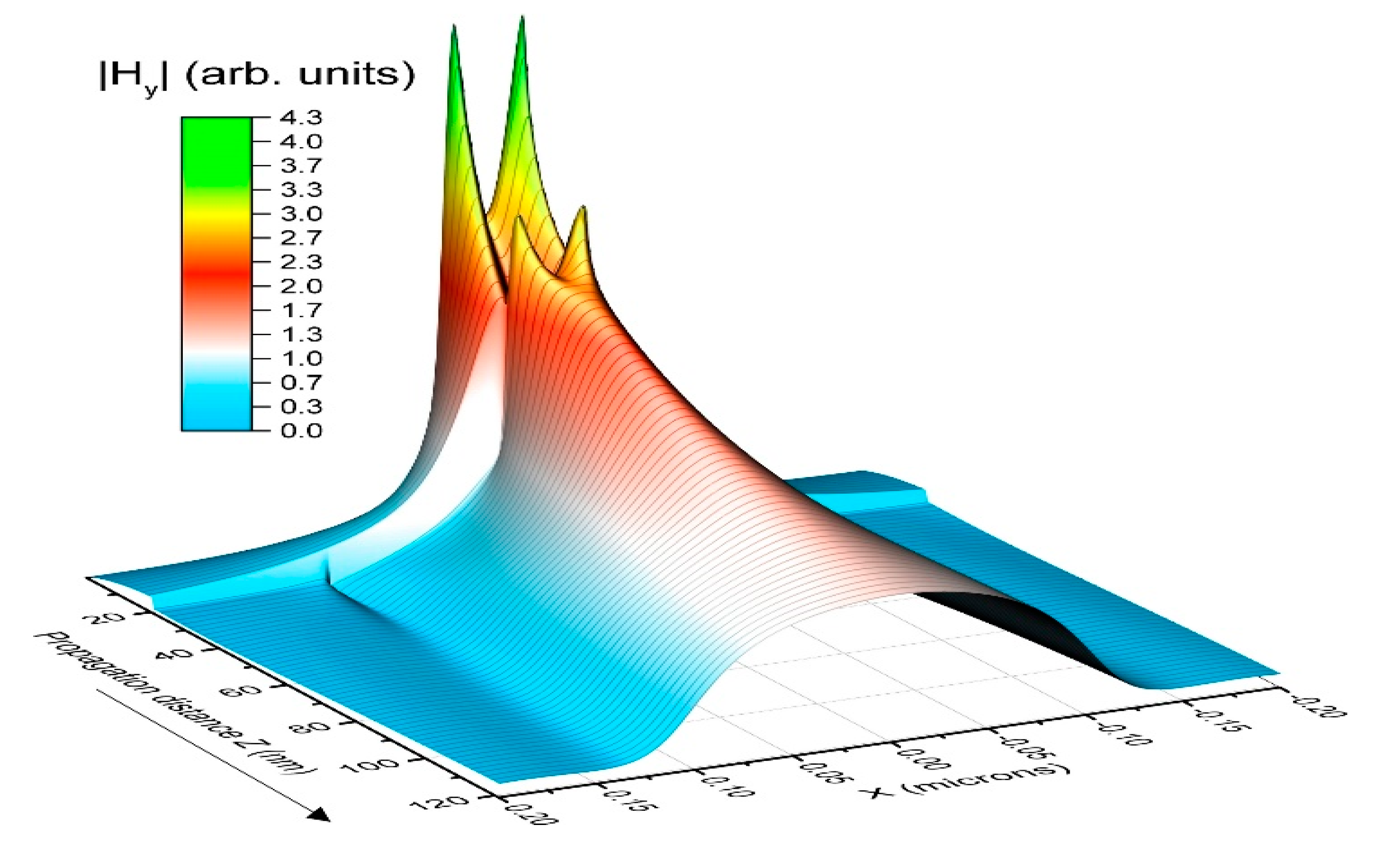
4.2. Butt-Coupling Between Plasmonic and Dielectric Waveguide

To validate further our proposed method, we considered the fundamental TM0 mode incident from a plasmonic waveguide upon a single mode dielectric waveguide as depicted in Figure 5.
Figure 6 illustrates the evolution of the total propagated magnetic field as it crosses the junction plane at Z = 20 nm, and ultimately evolves to the characteristic shape of the fundamental TM0 mode of the symmetric silicon guide. The parameters of the two guides assume the following values:
Number of sampling points along x-axis N = 218, sampling interval along the x-axis Δx = 0.1 nm, propagation step-size Δz = 1 nm, the propagation distance in the plasmonic and dielectric guides equals 20 and 100 nm respectively. The dielectric waveguide core thickness Wd = 220 nm, MIM waveguide core thickness Wp = 42 nm, Silicon refractive index nco = 3.477, metal refractive index (silver) ncl = 0.397 − j 11.4, and the free space wavelength λo = 1.55 µm. The contour plot depicted in Figure 7, shows the expansion of the confined light inside the plasmonic guide as it crosses the junction plane z = 0, and after almost 100 nm the characteristic TM0 mode of the dielectric guide is well established as shown in Figure 6.
The integration and merging of tightly confined waveguides, like plasmonic guides, and thin-film dielectric waveguides will be an essential technology for the development of extremely compact photonic components. Thus, numerical modeling and optimization of the power transmission efficiency is a key factor to increase device density in the implementation of photonic integrated circuits. Accordingly, we considered the butt-coupled plasmonic-MIM waveguide of Figure 5. Upon the incidence of the TM0 plasmonic mode from the MIM guide on the interface plane z = 0, a backward reflected field is generated. The total transmitted field (sum of the incident and reflected) constituting the guided, radiation and evanescent components is directly calculated from Equation (17). And the power transmission efficiency η is readily obtained from Equation (19) except Gr is replaced by Ht, that is:
  η   = ( | H t ( x ) H i * ( x ) d x | | H i ( x ) | 2 d x ) 2
The power transmission efficiency η of such coupler as function of the plasmonic guide core width Wp has been studied by [27], using a combined mode-matching and FDFD (finite-difference frequency domain). Figure 8 reveals good agreement between our results and those calculated by the (FDFD).
The numerical values of the BPM parameters are as follows: Number of sampling points along x-axis N = 216 with sampling interval Δx = 0.46 nm, propagation step-size Δz = 0.75Δx, propagation distances in the plasmonic and dielectric guides = 20 and 130 nm respectively, hence the total propagation distance =150 nm. The dielectric waveguide core thickness is kept constant Wd = 300 nm, the plasmonic waveguide core thickness Wp varies from 5 to 200 nm, Silicon refractive index nco = 3.477, metal refractive index (silver) ncl = 0.397 − j 11.4, and the free space wavelength λo = 1.55 µm.
The FFT-BPM gives a maximum power transmission when Wp ≅ 42 nm., which is the same width predicted by the FDFD. It is worthy to note that, at relatively long wavelengths (λo = 1.55 µm), and beyond Wp ≅ 42 nm; the light confinement characteristics of the MIM waveguide increases, and hence, the effective light-collection cross section of the plasmonic guide becomes much higher than the geometrical dimension of the insulating core. That is, the field penetration distance in the metal, around the air core, is much larger than the core width (42 nm) as pointed out in [27]. Hence, as Wp is increased beyond 42 nm, the transmission efficiency decreases as expected in Figure 8.

5. Conclusions

In this paper, we present a novel study of guided light beam reflection and transmission at different waveguide discontinuities and junctions using FFT-based BPM in TE and TM cases. Two remedies are introduced to circumvent the major difficulties that preclude the applicability of the FFT-based BPM in the investigation of TM fields. An equivalent index transforms the TM problem to a TE one, and the step-like index profile of the plasmonic and dielectric guides are smoothed via a sigmoid-like function. This enables full exploitation of the advantage and simplicity that distinguish the traditional split-step FFT-BPM. To the best of the authors’ knowledge, this scheme is proposed for the first time. An accurate combined spatial-spectral formalism is included in the FFT-BPM framework to calculate the reflected field at the junction plane between butt-coupled dielectric-plasmonic waveguides. The reflection characteristics of single layer and multilayer coatings at the facet of a dielectric waveguide are also investigated. The results fairly agree with previously published data. We claim that, the method can be extended to other types of interesting problems, like the transverse evanescent coupling between MIM-dielectric and MIM-MIM waveguides. Such coupling could be useful and efficient for nanoscale wavelength filters, ultra-fast optical switching and sensing, as well as graphene-based plasmonic devices.

Author Contributions

A.S. and L.R.G. performed calculations and writing. Y.-C.D. Review and Editing. All authors read and approved the final manuscript.

Funding

This study was partially funded by the Allied Advanced Intelligent Biomedical Research Center (A2IBRC) under the Higher Education Sprout Project of Ministry of Education.

Acknowledgments

The authors would like to thank the support from the National Center for Radiation Research (NCRRT) at Atomic Energy Authority in Egypt.

Conflicts of Interest

The authors declare no conflict of interest.

Abbreviations

FFT-BPM: FFT-based Beam Propagation Method; TE: Transverse Electric; TM: Transverse Magnetic; MIM: metal insulator metal; FDFD: finite difference frequency domain; TM0: transverse magnetics fundamental mode; PWE: plane wave expansion, TMM: Transfer Matrix Method.

References

  1. Li, E.P.; Chu, H.S. Plasmonic Nanoelectronics and Sensing; Cambridge University Press: Cambridge, UK, 2014. [Google Scholar]
  2. Kinsey, N.; Ferrera, M.; Shalaev, V.M.; Boltasseva, A. Examining nanophotonics for integrated hybrid systems: A review of plasmonic interconnects and modulators using traditional and alternative materials. JOSA B 2015, 32, 121–142. [Google Scholar] [CrossRef]
  3. Chen, J.; Badioli, M.; Alonso-González, P.; Thongrattanasiri, S.; Huth, F.; Osmond, J.; Spasenović, M.; Centeno, A.; Pesquera, A.; Godignon, P.; et al. Optical nano-imaging of gate-tunable graphene plasmons. Nature 2012, 487, 77–81. [Google Scholar] [CrossRef] [PubMed] [Green Version]
  4. Ni, G.X.; Wang, L.; Goldflam, M.D.; Wagner, M.; Fei, Z.; McLeod, A.S.; Liu, M.K.; Keilmann, F.; Özyilmaz, B.; Neto, A.H.C.; et al. Ultrafast optical switching of infrared plasmon polaritons in high-mobility graphene. Nat. Photonics 2016, 10, 244–247. [Google Scholar] [CrossRef]
  5. Basov, D.N.; Fogler, M.M.; De Abajo, F.J.G.; Fogler, M. Polaritons in van der Waals materials. Science 2016, 354, aag1992. [Google Scholar] [CrossRef]
  6. Koppens, F.H.L.; Chang, D.E.; De Abajo, F.J.G. Graphene Plasmonics: A Platform for Strong Light–Matter Interactions. Nano Lett. 2011, 11, 3370–3377. [Google Scholar] [CrossRef]
  7. Chen, L.; Shakya, J.; Lipson, M. Subwavelength confinement in an integrated metal slot waveguide on silicon. Opt. Lett. 2006, 31, 2133–2135. [Google Scholar] [CrossRef]
  8. Tang, L.; Kocabas, S.E.; Latif, S.; Okyay, A.K.; Ly-Gagnon, D.-S.; Saraswat, K.C.; Miller, D.A.B. Nanometre-scale germanium photodetector enhanced by a near-infrared dipole antenna. Nat. Photonics 2008, 2, 226–229. [Google Scholar] [CrossRef]
  9. Garcia-Vidal, F.J. Solid-state physics: Light at the end of the channel. Nature 2006, 440, 431–433. [Google Scholar] [CrossRef]
  10. Gomaa, L.R.; Shaaban, A.; Hameed, M.F.O.; Obayya, S.S.A. Competitiveness of the BPM in studying the optical beams at critical incidence on dielectric interfaces. Opt. Quantum Electron. 2017, 49, 51. [Google Scholar] [CrossRef]
  11. Shaaban, A.; Sayed, M.; Hameed, M.F.O.; Saleh, H.I.; Gomaa, L.; Du, Y.-C.; Obayya, S.; Obayya, S.A. Fast parallel beam propagation method based on multi-core and many-core architectures. Optik 2019, 180, 484–491. [Google Scholar] [CrossRef]
  12. Kaczmarski, P.; Lagasse, P. Bidirectional beam propagation method. Electron. Lett. 1988, 24, 675–676. [Google Scholar] [CrossRef]
  13. Shaaban, A.; Lotfy, R.G.; Du, Y.C. Adaptability of Bidirectional FFT-Based Beam propagation Method to investigate Dielectric-Plasmonic waveguide coupler. 2019, submitted. 2019. submitted. [Google Scholar]
  14. Franssens, G.; Kaczmarski, P.; Baets, R.; Lagasse, P. Extension of bidirectional beam propagation method to TM polarisation and application to laser facet reflectivity. Electron. Lett. 1989, 25, 716–717. [Google Scholar] [CrossRef]
  15. Vassallo, C. Difficulty with vectorial BPM. Electron. Lett. 1997, 33, 61–62. [Google Scholar] [CrossRef]
  16. Hoekstra, H.J.W.M.; Lambeck, P.V.; Krijnen, G.J.; Ctvroky, J.; De Minicis, H.; Sibilia, C.; Conradi, O.; Helfert, S.; Pregla, R. A COST 240 benchmark test for beam propagation methods applied to an electrooptical modulator based on surface plasmons. J. Lightwave Technol. 1998, 16, 1921–1927. [Google Scholar] [CrossRef]
  17. Poladian, L.; Ladouceur, F. Unification of TE and TM beam propagation algorithms. IEEE Photonics Technol. Lett. 1998, 10, 105–107. [Google Scholar] [CrossRef]
  18. Yamauchi, J.; Shimada, N.; Nito, Y.; Nakano, H. Transverse-magnetic BPM analysis of a step-index slab waveguide expressed by a sigmoid function. IEEE Photonics Technol. Lett. 2009, 21, 149–151. [Google Scholar] [CrossRef]
  19. Smartt, C.; Benson, T.; Kendall, P. ‘Free space radiation mode’ method for the analysis of propagation in optical waveguide devices. IEE Proc. J Optoelectron. 1993, 140, 56–61. [Google Scholar] [CrossRef]
  20. Wu, S.; Xiao, J. A pseudospectral reflective beam propagation method for optical waveguides. IEEE Photonics Technol. Lett. 2017, 29, 435–438. [Google Scholar] [CrossRef]
  21. Manenkov, A.B.; Latsas, G.P.; Tigelis, I.G. Scattering of the transverse magnetic modes from an abruptly ended strongly asymmetrical slab waveguide by an accelerated integral equation technique. J. Opt. Soc. Am. A 2001, 18, 3110. [Google Scholar] [CrossRef]
  22. Vassallo, C. Reflectivity of multidielectric coatings deposited on the end facet of a weakly guiding dielectric slab waveguide. J. Opt. Soc. Am. A 1988, 5, 1918. [Google Scholar] [CrossRef]
  23. Smartt, C.; Benson, T.; Kendall, P. Exact analysis of waveguide discontinuities: Junctions and laser facets. Electron. Lett. 1993, 29, 1352–1353. [Google Scholar] [CrossRef]
  24. Nguyen, T.G.; Mitchell, A. Analysis of optical waveguides with multilayer dielectric coatings using plane wave expansion. J. Lightwave Technol. 2006, 24, 635–642. [Google Scholar] [CrossRef]
  25. Yamauchi, J.; Kanbara, H.; Nakano, H. Analysis of optical waveguides with high-reflection coatings using the FD-TD method. IEEE Photonics Technol. Lett. 1998, 10, 111–113. [Google Scholar] [CrossRef] [Green Version]
  26. Orfanidis, S.J. Electromagnetic Waves and Antennas; Rutgers University: Piscataway, NJ, USA, 2008. [Google Scholar]
  27. Veronis, G.; Fan, S. Theoretical investigation of compact couplers between dielectric slab waveguides and two-dimensional metal-dielectric-metal plasmonic waveguides. Opt. Express 2007, 15, 1211–1221. [Google Scholar] [CrossRef] [PubMed] [Green Version]
Figure 1. Schematic diagram of a 2-dimensional waveguide facet terminated by air.
Applsci 09 04362 g001
Figure 2. The power reflectivity curve comparison between our proposed method and Vassallo [15], and plane wave expansion (PWE) techniques [24] at (a) transverse electric (TE) polarization case, (b) transverse magnetic (TM) polarization case.
Applsci 09 04362 g002
Figure 3. Power reflectivity of single layer antireflection coating as function of coating thickness u. The minimum at u = 0.206 µm agrees with accurate previously published results.
Applsci 09 04362 g003
Figure 4. The power reflectivity as function of the wavelength of a multilayer coating made of 6 layers each having a thickness λ/4.
Applsci 09 04362 g004
Figure 5. Butt-coupled metal-insulator-metal (MIM) and dielectric waveguides.
Applsci 09 04362 g005
Figure 6. Evolution of the magnetic field Hy of the fundamental mode in the plasmonic guide as it propagates towards the silicon guide where the symmetric TM0 mode is well established after almost 100 nm.
Applsci 09 04362 g006
Figure 7. The confined TM0 mode of the plasmonic guide expands inside the silicon core of width Wd, where the symmetric TM0 mode is well established after almost 100 nm.
Applsci 09 04362 g007
Figure 8. The percentage of the transmitted power η compared with reference [27]. As the plasmonic waveguide width Wp increases beyond 42 nm (point of maximum η), the light-collection cross section of the plasmonic guide becomes much higher than the geometrical dimension of the insulating layer, thus η decreases.
Applsci 09 04362 g008

