Area-Efficient FFT Kernel with Improved Use of GI for Multistandard MIMO-OFDM Applications


Abstract
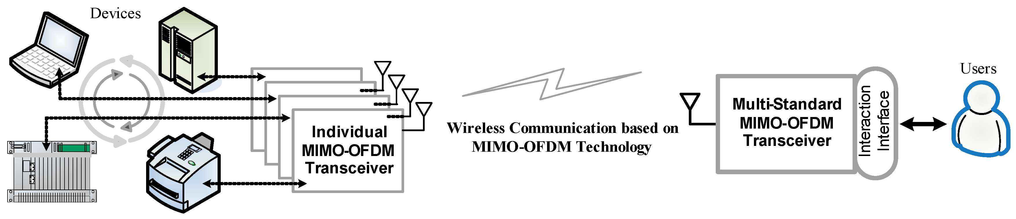
1. Introduction
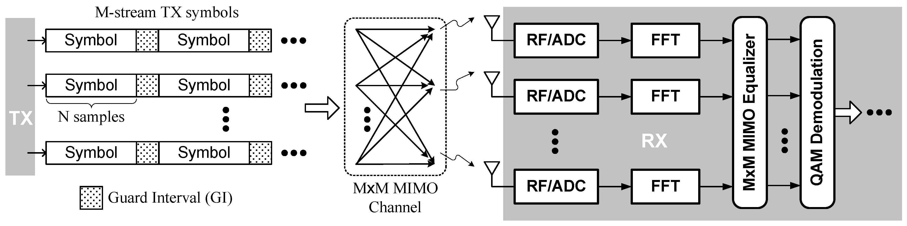
2. FFT Design Considerations
2.1. Related Works for MIMO-OFDM FFT
2.2. Kernel-Based FFT for Multiple Standards
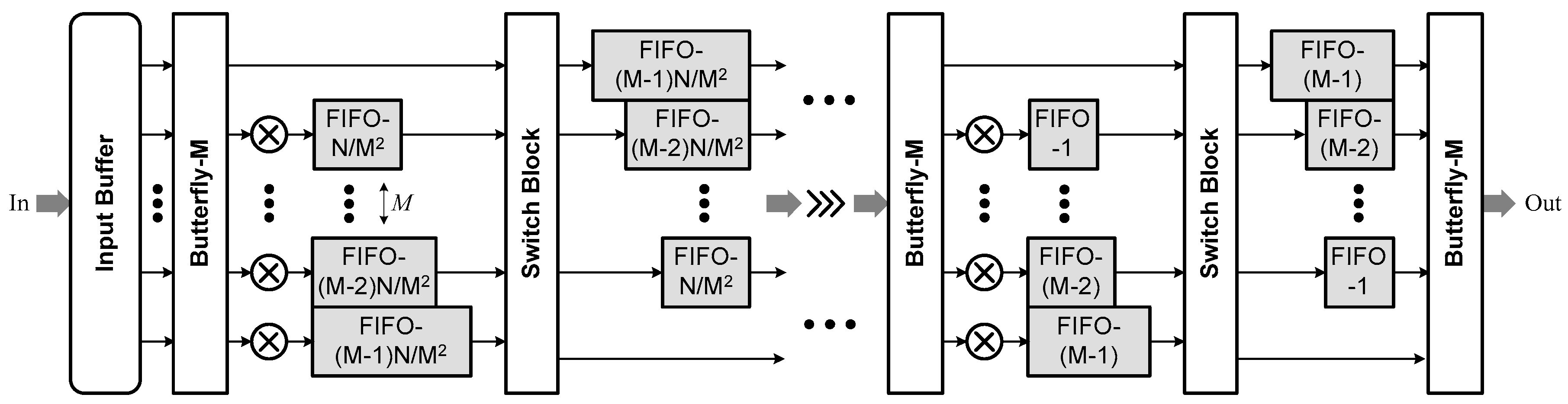
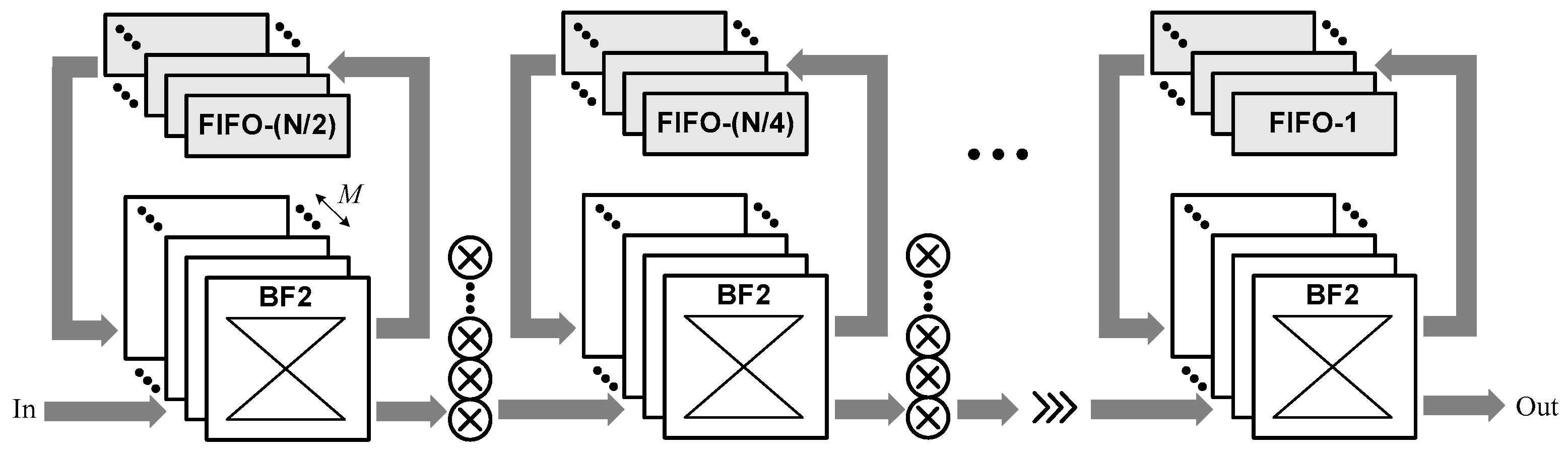
3. Proposed FFT Kernel Architecture
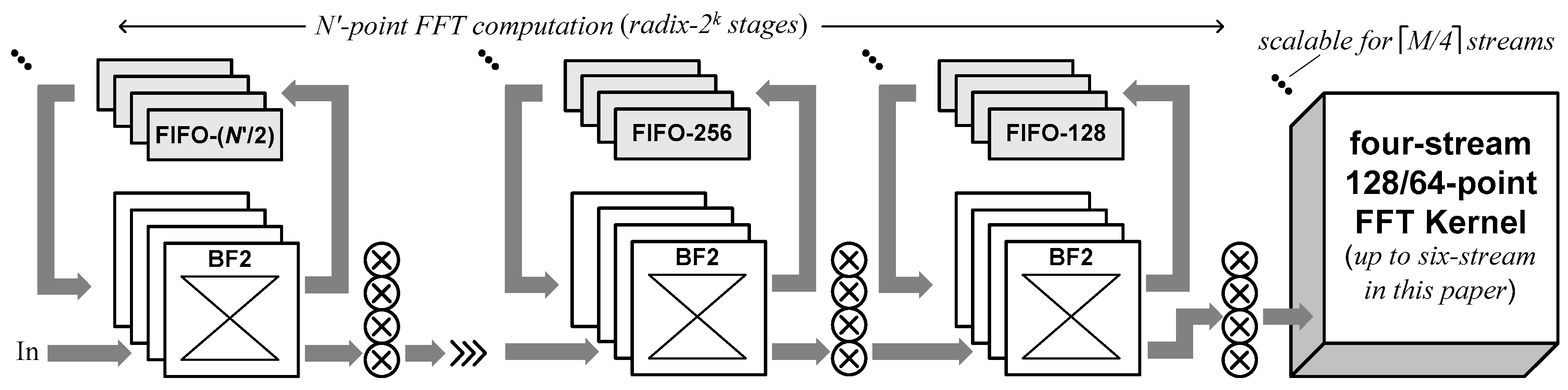
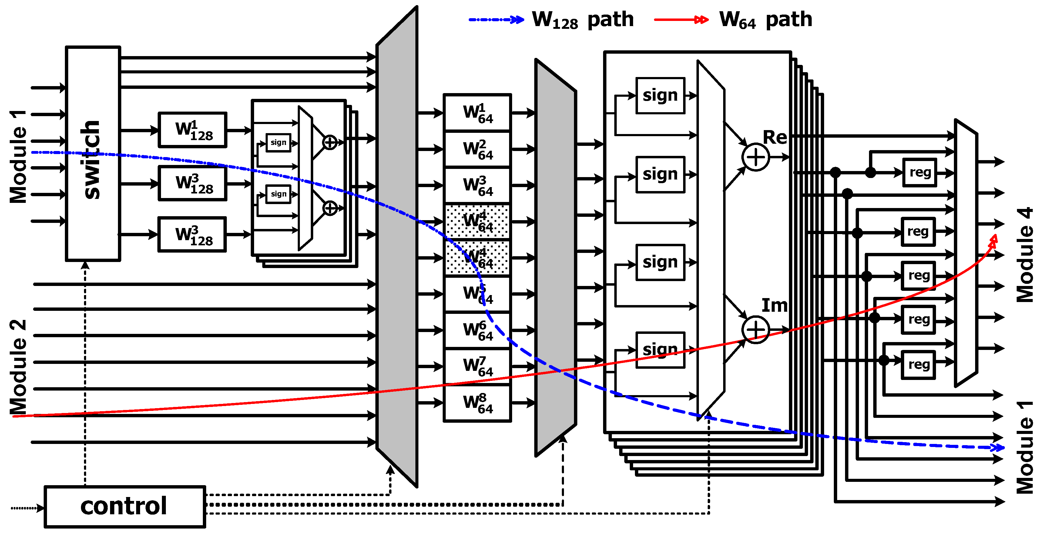
3.1. Algorithm and Architecture Overview
- (i)
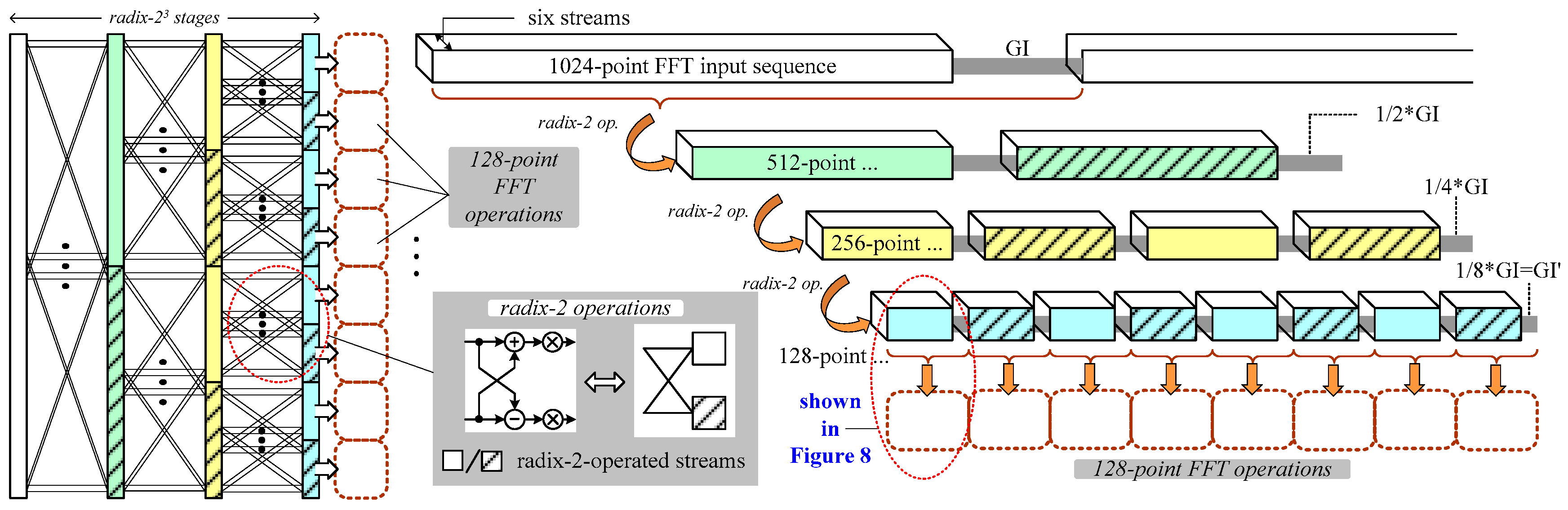
- In mixed-multipath operations based on streams or radix-8, GI duration can be employed to conduct 128-point FFT operations in up to six streams.
- (ii)
- Resource sharing is applied to multipath radix-2/8/8 operations by using an area-reduced constant multiplication unit.
- (iii)
- The required memory size (i.e., the number of stored data elements) are maintained at a modest level by using a sophisticated sorting scheme applied to the buffer.
- (iv)
3.2. Architecture Modules
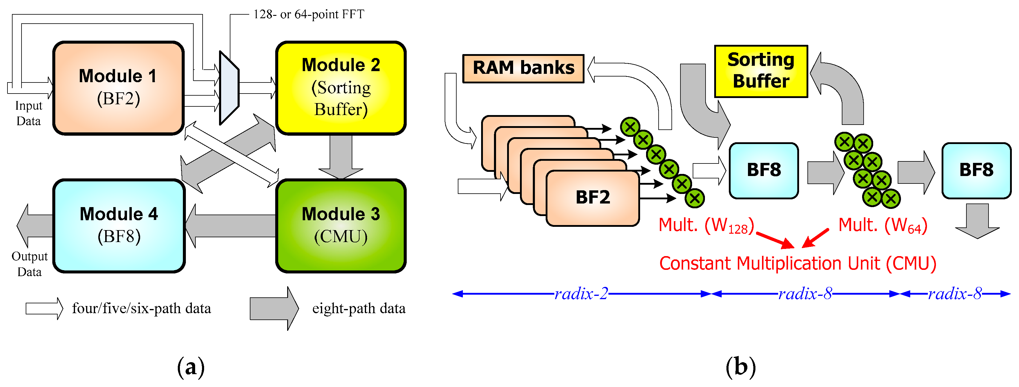
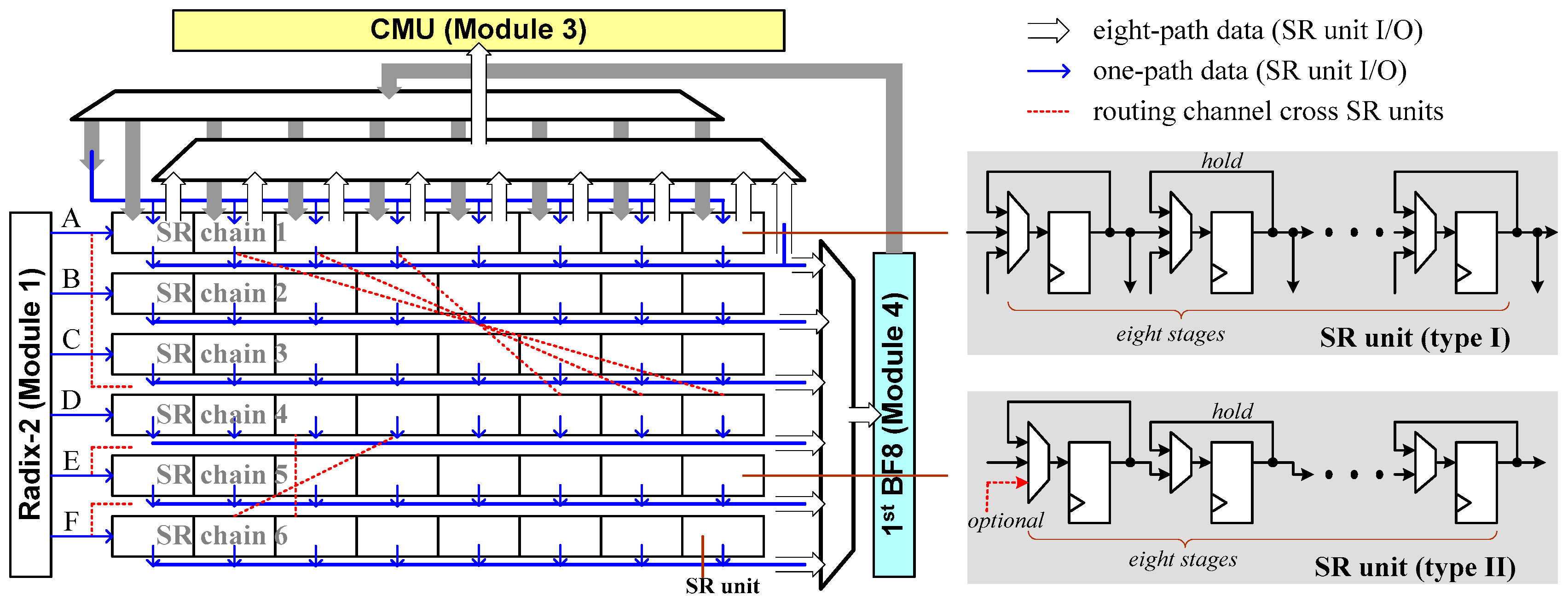
3.2.1. Module 1
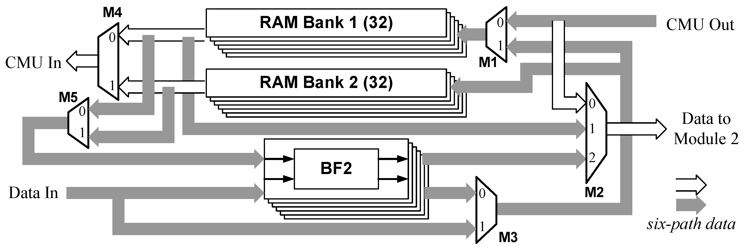
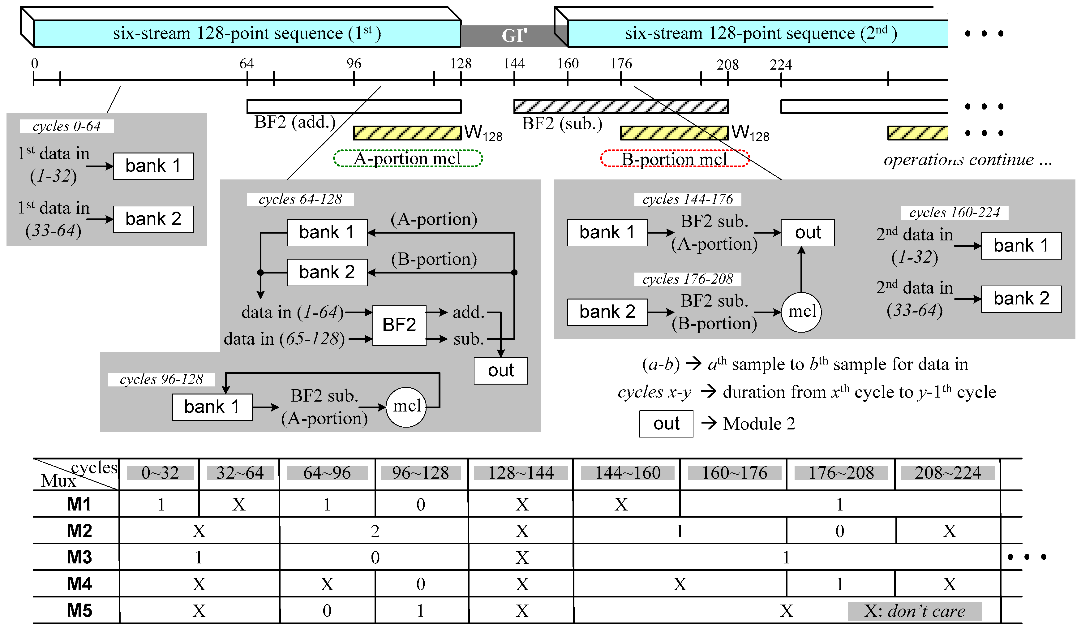
3.2.2. Module 2
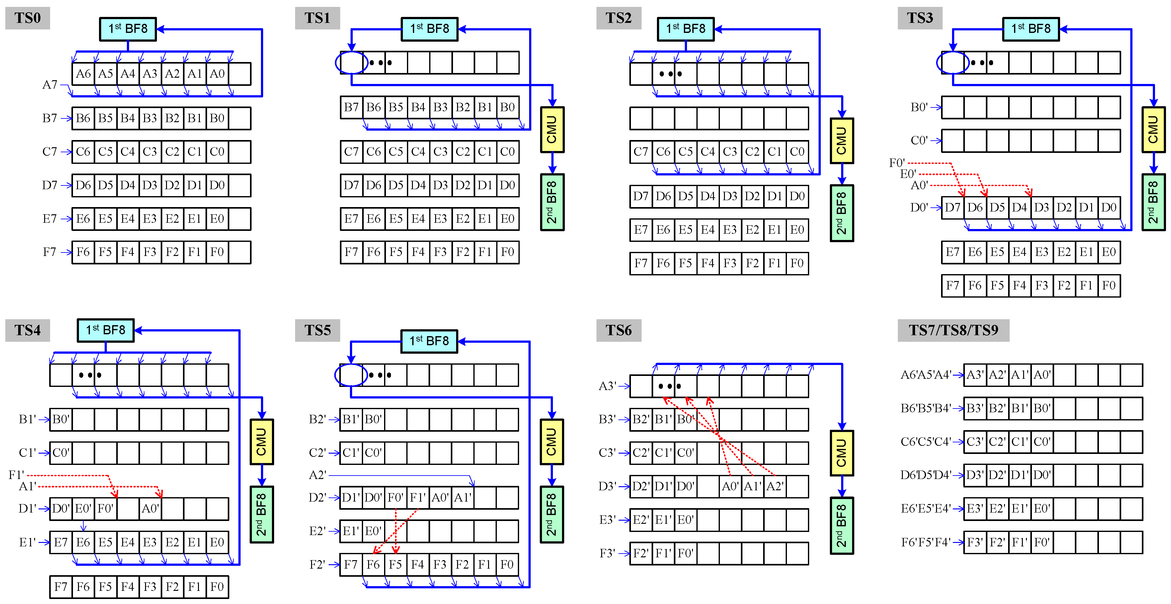
3.2.3. Module 3
3.2.4. Module 4
4. Results and Comparison
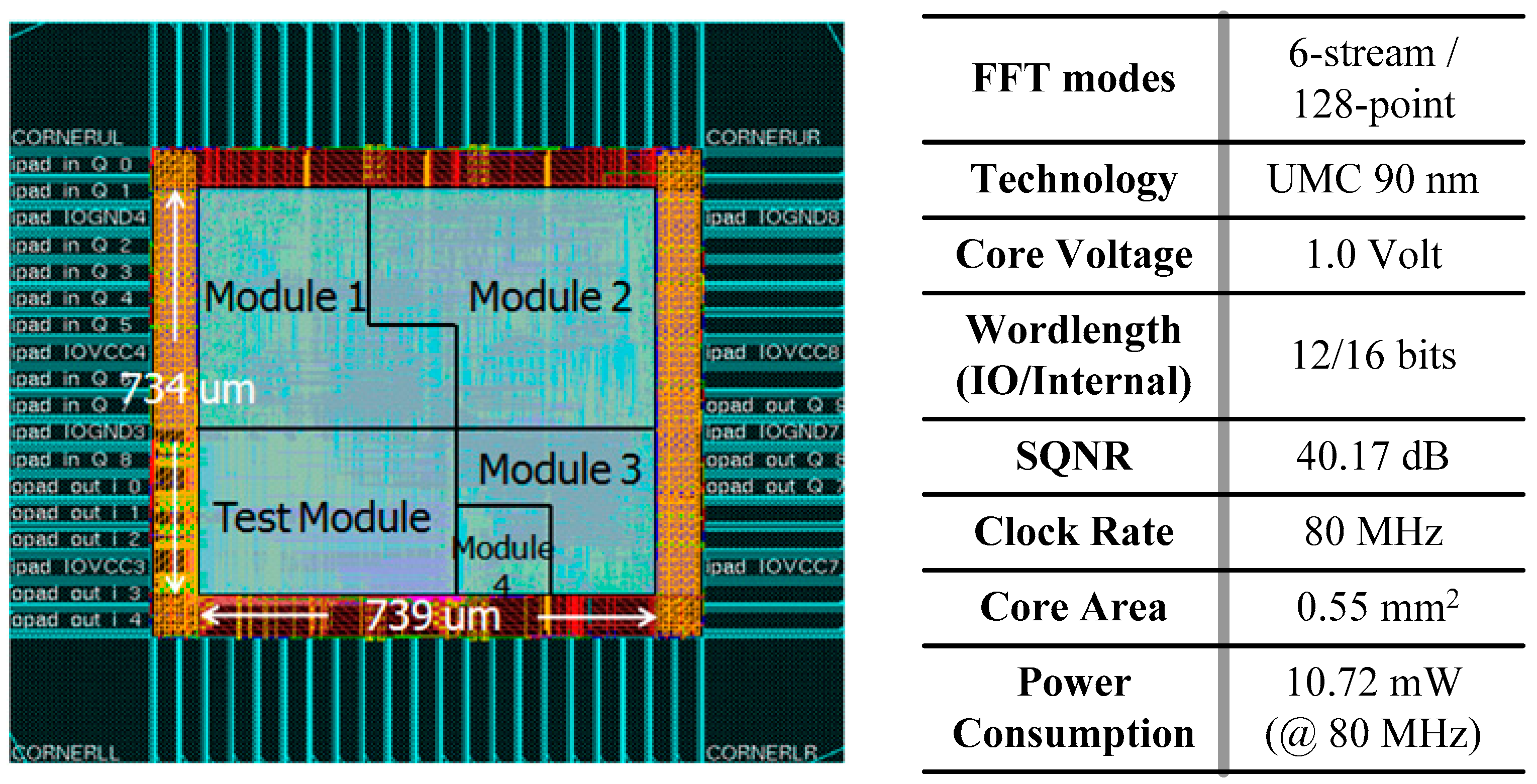
4.1. Design Implementation
4.2. Comparison
5. Conclusions
Author Contributions
Funding
Acknowledgments
Conflicts of Interest
References
- Yang, H.A. Road to future broadband wireless access: MIMO-OFDM-based air interface. IEEE Commun. Mag. 2005, 43, 53–60. [Google Scholar] [CrossRef]
- Panajotović, A.; Riera-Palou, F.; Femenias, G. Adaptive uniform channel decomposition in MU-MIMO-OFDM: Application to IEEE 802.11ac. IEEE Trans. Wirel. Commun. 2015, 14, 2896–2910. [Google Scholar] [CrossRef]
- Ketonen, J.; Juntti, M.; Cavallaro, J.R. Performance—complexity comparison of receivers for a LTE MIMO–OFDM system. IEEE Trans. Signal Process. 2010, 58, 3360–3372. [Google Scholar] [CrossRef]
- Dahlman, E.; Parkvall, S.; Skold, J. 4G—LTE-Advanced Pro and the Road to 5G; Academic Press: Cambridge, MA, USA, 2016. [Google Scholar]
- Parkvall, S.; Dahlman, E.; Furuskar, A.; Frenne, M.N.R. The new 5G radio access technology. IEEE Commun. Stand. Mag. 2017, 1, 24–30. [Google Scholar] [CrossRef]
- Ali, A.; Hamouda, W. A multi-mode IFFT/FFT processor for IEEE 802.11ac: Design and implementation. Wirel. Commun. Mob. Comput. 2016, 16, 1713–1725. [Google Scholar] [CrossRef]
- Yang, C.H.; Yu, T.H.; Marković, D. Power and area minimization of reconfigurable FFT processors: A 3GPP-LTE example. IEEE J. Solid-State Circuits 2012, 47, 1–12. [Google Scholar] [CrossRef]
- Baas, B.M. A low-power, high-performance, 1024-point FFT processor. IEEE J. Solid-State Circuits 1999, 34, 380–387. [Google Scholar] [CrossRef]
- Shousheng, H.; Torkelson, M. Designing pipeline FFT processor for OFDM (de)modulation. In Proceedings of the URSI International Symposium on Signals, System, and Electron, Pisa, Italy, 22 October 1998; pp. 257–262. [Google Scholar]
- Jo, B.G.; Sunwoo, M.H. New continuous-flow mixed radix (CFMR) FFT using novel in-place strategy. IEEE Trans. Circuits Syst. Part I Regul. Pap. 2005, 52, 911–919. [Google Scholar] [CrossRef]
- Chen, C.M.; Hung, C.C.; Huang, Y.H. An energy-efficient partial FFT processor for the OFDMA communication system. IEEE Trans. Circuits Syst. II Express Briefs 2010, 57, 136–140. [Google Scholar] [CrossRef]
- Mohanty, B.K.; Meher, P.K. Area-delay-energy efficient VLSI architecture for scalable in-place computation of FFT on real data. IEEE Trans. Circuits Syst., Part-I Regul. Pap. 2019, 66, 1042–1050. [Google Scholar] [CrossRef]
- Tang, S.N.; Jan, F.C.; Cheng, H.W.; Lin, C.K.; Wu, G.Z. Multimode memory-based FFT processor for wireless display FD-OCT medical systems. IEEE Trans. Circuits Syst. I Regul. Pap. 2014, 61, 3394–3406. [Google Scholar] [CrossRef]
- Xing, Q.J.; Ma, Z.G.; Xu, Y.K. A novel conflict-free parallel memory access scheme for FFT processors. IEEE Trans. Circuits Syst. II Express Briefs 2017, 64, 1347–1351. [Google Scholar] [CrossRef]
- Liu, S.; Liu, D. A high-flexible low-latency memory-based FFT processor for 4G, WLAN, and future 5G. IEEE Trans. Very Large Scale Integr. (VLSI) Syst. 2018, 27, 511–523. [Google Scholar] [CrossRef]
- Hwang, Y.T.; Chen, Y.J.; Chen, W.D. Scalable FFT Kernel designs for MIMO OFDM based communication systems. In Proceedings of the IEEE Conferrence TENCON, Taipei, Taiwan, 30 October–2 November 2007; pp. 1–4. [Google Scholar]
- Hung, C.L.; Long, S.S.; Shiue, M.T. A low power and variable-length FFT processor design for flexible MIMO OFDM systems. In Proceedings of the IEEE International Symposium on Circuits and System (ISCAS), Taipei, Taiwan, 24–27 May 2009; pp. 705–708. [Google Scholar]
- Chen, S.G.; Huang, S.J.; Garrido, M.; Jou, S.J. Continuous-flow parallel bit-reversal circuit for MDF and MDC FFT architectures. IEEE Trans. Circuits Syst. I Reg. Pap. 2014, 61, 2869–2877. [Google Scholar] [CrossRef]
- Lin, Y.T.; Tsai, P.Y.; Chiueh, T.D. Low-power variable length fast Fourier transform processor. Proc. IEE Comput. Dig. Tech. 2005, 152, 499–506. [Google Scholar] [CrossRef]
- Yang, K.J.; Tsai, S.H.; Chuang Gene, C.H. MDC FFT/IFFT processor with variable length for MIMO-OFDM systems. IEEE Trans. Very Large Scale Integr. (VLSI) Syst. 2013, 21, 720–731. [Google Scholar] [CrossRef]
- Fu, B.; Ampadu, P. An area efficient FFT/IFFT processor for MIMO OFDM WLAN 802.11n. J. Signal Process. Syst. 2009, 56, 59–68. [Google Scholar] [CrossRef]
- Locharla, G.R.; Mahapatra, K.K.; Ari, S. Variable length mixed radix MDC FFT/IFFT processor for MIMO-OFDM application. IET Comput. Digit. Tech. 2018, 12, 9–19. [Google Scholar] [CrossRef]
- Yoshizawa, S.; Orikasa, A.; Miyanaga, Y. An area and power efficient pipeline FFT processor for 8×8 MIMO-OFDM systems. In Proceedings of the IEEE International Symposium on Circuits and System (ISCAS), Rio de Janeiro, Brazil, 15–19 May 2011; pp. 2705–2708. [Google Scholar]
- Lin, Y.W.; Liu, H.Y.; Lee, C.Y. A 1-GS/s FFT/IFFT processor for UWB applications. IEEE J. Solid-State Circuits 2005, 40, 1726–1735. [Google Scholar] [CrossRef]
- Lin, Y.W.; Lee, C.Y. Design of an FFT/IFFT processor for MIMO OFDM systems. IEEE Trans. Circuits Syst. I Reg. Pap. 2007, 54, 807–815. [Google Scholar] [CrossRef]
- Liu, H.; Lee, H. A high performance four-parallel 128/64-point radix-24 FFT/IFFT processor for MIMO-OFDM systems. In Proceedings of the IEEE Asia Pacific Conference on Circuits and System (APCCAS), Macao, China, 30 November–3 December 2008; pp. 834–837. [Google Scholar]
- Chen, Y.; Lin, Y.W.; Taso, Y.C.; Lee, C.Y. A 2.4-Gsample/s DVFS FFT processor for MIMO OFDM communication systems. IEEE J. Solid-State Circuits 2008, 43, 1260–1273. [Google Scholar] [CrossRef]
- Tang, S.N.; Liao, C.H.; Chang, T.Y. An area- and energy-efficient multimode FFT processor for WPAN/WLAN/WMAN systems. IEEE J. Solid-State Circuits 2012, 47, 1419–1437. [Google Scholar] [CrossRef]
- Liu, L.; Ren, J.; Wang, X.; Ye, F. Design of low-power, 1GS/s throughput FFT processor for MIMO-OFDM UWB communication system. In Proceedings of the IEEE International Symposium Circuits and System (ISCAS), New Orleans, LA, USA, 27–30 May 2007; 2007; pp. 2594–2597. [Google Scholar]
- Oh, J.Y.; Lim, M.S. Area and power efficient pipeline FFT algorithm. In Proceedings of the IEEE Workshop on Signal Processing Systems (SiPS), Athens, Greece, 2–4 November 2005; pp. 520–525. [Google Scholar]
- Mahdavi, M.; Edfors, O.; Öwall, V.; Liu, L. A low latency FFT/IFFT architecture for massive MIMO systems utilizing OFDM guard bands. IEEE Trans. Circuits Syst. I Reg. Pap. 2019, 66, 2763–2774. [Google Scholar] [CrossRef]
- Maharatna, K.; Grass, E.; Jagdhold, U. A 64-point Fourier transform hip for high-speed wireless LAN application using OFDM. IEEE J. Solid-State Circuits 2004, 39, 484–493. [Google Scholar] [CrossRef]
- Tang, S.N.; Tsai, J.W.; Chang, T.Y. A 2.4 GS/s FFT processor for OFDM based WPAN applications. IEEE Trans. Circuits Syst. II Express Briefs 2010, 57, 451–455. [Google Scholar] [CrossRef]


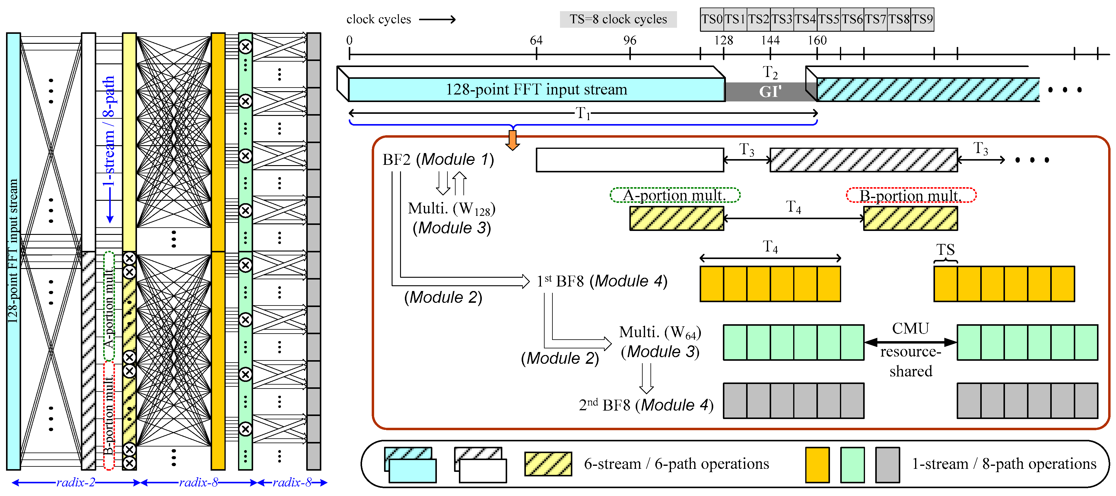
| GI’ Clock Cycles | No. of Streams (max.) | T1 Clock Cycles | T2 Clock Cycles | T3 Clock Cycles | T4 Clock Cycles |
|---|---|---|---|---|---|
| 32 (1/4 symbol) | 6 | 160 | 32 | 16 | 48 (6 TS) |
| 16 (1/8 symbol) | 5 | 144 | 16 | 8 | 40 (5 TS) |
| 0 (None) | 4 | 128 | 0 | 0 | 32 (4 TS) |

| [25] | [30] (ref.) | [21] | Proposed | |
|---|---|---|---|---|
| Architecture | MRMDF | R-24 SDF | MDC | MRM2DF |
| Technology | 0.13 µm | 90 nm | 0.18 µm | 90 nm |
| No. stream (path) | 4 | 4 | 4 | 6 |
| Clock rate (MHz) | 40 | 80 | 75 | 80 |
| Nor. core area3 (mm2) | 0.67 1 | 0.54 | 0.525 2 | 0.55 1 |
| Throughput (R: clock rate) | 4R | 4R | 4R | 6R (six streams) |
| Throughput per area (R/mm2) | 5.97 | 7.41 | 7.62 | 10.91 |
© 2019 by the authors. Licensee MDPI, Basel, Switzerland. This article is an open access article distributed under the terms and conditions of the Creative Commons Attribution (CC BY) license (http://creativecommons.org/licenses/by/4.0/).
Share and Cite
Tang, S.-N.; Chen, Y.-H. Area-Efficient FFT Kernel with Improved Use of GI for Multistandard MIMO-OFDM Applications. Appl. Sci. 2019, 9, 2877. https://doi.org/10.3390/app9142877
Tang S-N, Chen Y-H. Area-Efficient FFT Kernel with Improved Use of GI for Multistandard MIMO-OFDM Applications. Applied Sciences. 2019; 9(14):2877. https://doi.org/10.3390/app9142877
Chicago/Turabian StyleTang, Song-Nien, and Yuan-Ho Chen. 2019. "Area-Efficient FFT Kernel with Improved Use of GI for Multistandard MIMO-OFDM Applications" Applied Sciences 9, no. 14: 2877. https://doi.org/10.3390/app9142877
APA StyleTang, S.-N., & Chen, Y.-H. (2019). Area-Efficient FFT Kernel with Improved Use of GI for Multistandard MIMO-OFDM Applications. Applied Sciences, 9(14), 2877. https://doi.org/10.3390/app9142877