Review

Potential of Liquid-Crystal Materials for Millimeter-Wave Application

Department of Intelligent Mechatronics, Faculty of Systems Science and Technology, Akita Prefectural University, Yurihonjyo, Akita 015-0055, Japan
*
Author to whom correspondence should be addressed.
Appl. Sci. 2018, 8(12), 2544; https://doi.org/10.3390/app8122544
Submission received: 31 October 2018 / Revised: 28 November 2018 / Accepted: 3 December 2018 / Published: 8 December 2018
(This article belongs to the Special Issue Liquid Crystal THz Photonics: Materials, Devices and Applications)

Abstract

:
In this study, we reviewed three topics regarding the application of liquid-crystal (LC) materials to millimeter-wave (MMW) devices. It is essential to develop useful measurement methods for refractive indices of LC materials in the MMW region. Herein, a novel measurement method using optical short is demonstrated using a Si semiconductor substrate. There are two approaches to develop MMW LC devices. One is the quasi-optical approach, which involves scaling up the optical components, and the other approach involves integrating the LC materials into high-frequency electric circuits. A three-dimensional (3D) printer is used to fabricate the Fresnel lens, which is a typical quasi-optical device useful in the MMW region, where we can develop the tunable lens by introducing LC materials. A planar-type MMW waveguide is advantageous for integrating the LC materials to develop LC MMW devices using the second approach. We investigated a useful microstrip-line-type LC phase shifter by developing a novel conversion circuit to introduce the LC material onto the dielectric substrate surface. A phase shifter is an important MMW component that is used to attain a phased array antenna system, and a minimal twin antenna array is demonstrated using the microstrip-line-type LC phase shifters.

1. Introduction

Liquid crystals (LCs) are well known as excellent electro-optic materials, and their potential is sufficiently proven when we see the industrial success of the flat-panel display application. An LC device exhibits compactness, lightweight, low power consumption, and low driving voltage for all application fields in the optics and photonics [1,2,3,4,5,6,7,8,9,10,11,12,13,14,15,16,17,18]. Furthermore, some optical control devices, such as variable focusing lenses, beam-steering prisms, and polarization control devices, gained attention in conjunction with conventional LC device applications, such as spatial light modulators and phase shifters [12,13,14,15,16,17,18]. Recently, it became evident that LC materials have a large birefringence in the wider frequency range of the electromagnetic wave spectra, such as microwave, millimeter wave (MMW), and THz regions [19,20,21,22].
The novel frequency regions, which exist between the radio frequency and optics region, were forbidden for a long time because of the technological difficulties, i.e., even the very basic technologies, such as signal generation and detection, were insufficient for consumer applications. However, technological innovation occurred in the THz-sensing technology field upon using the femtosecond laser and photoconductive switch, and the unexplored frequency region including the MMW region gained attention from the high expectation of new application fields.
Furthermore, the next-generation wireless communication standard (i.e., 5G) recently became a popular topic of information and communications technology (ICT). The 5G technology exhibits an extremely short delay time and massive connectivity in conjunction with high-speed communication potential; thus, many people expect that many novel technologies leading to business opportunities will appear beyond smart phones. However, the frequency resources available for wireless communication were successively endangered after mobile phones came into existence, because the number of wireless terminals and the communication traffic increased steeply upon every generation change in the wireless communication standard. It is difficult to achieve the extremely high performance of 5G within the current frequency resources; thus, unexplored higher-frequency regions (i.e., MMW) enter the picture to realize 5G for many novel consumer services.
MMW can propagate with narrow beams using a small antenna, bringing some advantages for energy saving and data security. However, some types of beam control device are mandatory for MMW usage, and low-cost and manageable devices for MMW propagation control are essential for the usage of MMW to become common in our daily life. We believe that LC materials are primary candidates to attain such devices if we reevaluate the technological success history of LC materials in optics. It is evident that LC materials have generally large birefringence in the MMW region as compared to that in the optics region, which is key for attaining variable LC devices working in a specific frequency region. However, molecules of all the commercially available LC materials are designed for display applications, and there is almost no information about their properties in the MMW region. It is essential to develop efficient measurement methods for LC materials to collect more information about excellent LC materials in the MMW region [23,24,25,26,27].
A uniform LC molecular alignment must be maintained in the measurement to evaluate the anisotropy of the LC materials; thus, we investigated a measurement method using a rectangular waveguide combined with a magnetic field [25,26]. However, the amount of required LC material is still large, even though the waveguide size becomes smaller in the MMW region. We tried introducing the planar cell structure by using a coplanar waveguide (CPW) to significantly reduce the amount of test sample required [27]. In this case, another problem occurs; the inserted metal plate, which works as a moving electrical short, destroys the LC molecular alignment layer in one measurement. Firstly, a recent study to overcome this problem using a photo-induced electric short is reviewed. When a suitably strong light is irradiated on the intrinsic semiconductor wafer, the wafer becomes an excellent miller for THz waves due to the densely created photo carriers on the surface [28,29]. We fabricated a CPW by using an intrinsic Si wafer as a dielectric material, and the diode laser light was irradiated on a part of the waveguide to create a dense photo-carrier domain that could work as a moving reflection boundary of the MMW without any mechanical contacts.
There are two approaches to develop MMW control devices using LC materials. One involves scaling up the LC optical devices according to the increase in wavelength; these are called quasi-optical devices [30,31,32]. Although the device structure in this approach allows one to simply attain a specific functionality, an extremely thick LC layer is required because the wavelength of the MMW is at least one thousand times that of the optics region. A simple scale up of the LC layer causes fatal degradation of the response speed; thus, we tried introducing a polymer-dispersed LC (PDLC) structure, which consists of a large number of tiny integrated LC cells, by using porous polymethylmethacrylate (PMMA) materials [33,34,35]. We investigated the MMW Fresnel lens, which is a typical quasi-optical device and can be tunable by introducing LC materials. In this case, some kind of machinery process is essential for attaining the Fresnel structure, and direct machining of the bulky porous PMMA material was demonstrated [35]. If we use a Fresnel structural substrate, the spray deposition method of the porous PMMA is acceptable for attaining a bulky LC layer. In the next section, it is demonstrated that three-dimensional (3D) printers are precise enough to fabricate the Fresnel lens substrate, which becomes the base of the LC Fresnel lens working for MMW control.
Another approach to obtainan MMW LC device is the integration of LC materials into high-frequency electric circuits. The thickness of the LC layer can be significantly reduced if we choose a planar-type waveguide, because we can adopt the conventional sandwich cell structure to attain the LC devices. However, some extra parts must be integrated at the same time as the LC material to complete specific functionality, which leads to a complicated device structure in comparison with the quasi-optical approach. Many types of LC phase shifters, which are one of the important parts for integration circuits, were investigated by integrating the LC material into a suitable waveguide, such as a metal hollow waveguide [20,21,22,36,37,38], microstrip line [39,40,41,42,43,44,45,46,47,48,49,50], or coplanar waveguide [51,52,53].
In this study, we investigated a planar-type LC phase shifter using a microstrip line. A microstrip line is a very common planar waveguide, which has a large technological background based on its long history. Additionally, we also integrated an LC driving circuit, power divider, frequency elimination filter, and antennas in conjunction with the LC phase shifter to attain specific functional devices, such as a phased array antenna. However, it is normally useless to integrate the LC materials on the microstrip line, because the MMW propagates inside the dielectric material of the substrate. We investigated a novel conversion circuit that can switch the propagation path of the MMW between the dielectric substrate and the upper LC layer to allow the introduction of the LC material onto the surface [47,48,49,50]. In the last section, we describe the basic performance of a minimal twin array of LC phase shifters connected with a planar antenna.

2. Measurement of Complex Refractive Indices in Millimeter Wave

Most simple and common measurement methods of the refractive index in the MMW region involve introducing an LC material into any type of excellent waveguide and extracting the influence of LC materials by comparing the transmission properties with and without the test sample. The differential measurement of the transmission property caused by the successive small changes of the LC propagation length is a more precise measurement method called the cutback technique, which can eliminate the influence due to aspects other than the LC test material. We developed a measurement method for LC materials using a rectangular waveguide by inserting and moving a metal-tip electrical short, which can precisely change the propagation length of the LC material. A magnetic field was applied during the measurement to align the LC molecules uniformly, which is important for the LC measurement to evaluate its anisotropy [25,26]. Although the size of the waveguide becomes small in the MMW region, the mm-size cavity is still extremely large, based on common knowledge of the LC display application. If we utilize aplanar-type waveguide, such as a CPW, the test sample volume can be greatly reduced because a thinner sandwich cell structure can be introduced, such as in an LC display [27]. However, a metal plate, which works as a reflector of MMW and can change the LC length, must be in contact with the inner surface of the LC cell. The mechanical contact with the internal surface disrupts the LC molecular alignment layer after one measurement. In this section, we try utilizing an optical short, which can work as a moving reflector of the MMW without any mechanical contacts, where the CPW was fabricated using an intrinsic semiconductor, and the electrical short was created by photo-excited carriers. Experiments for the verification of the novel measurement method were performed using the Si substrate itself.

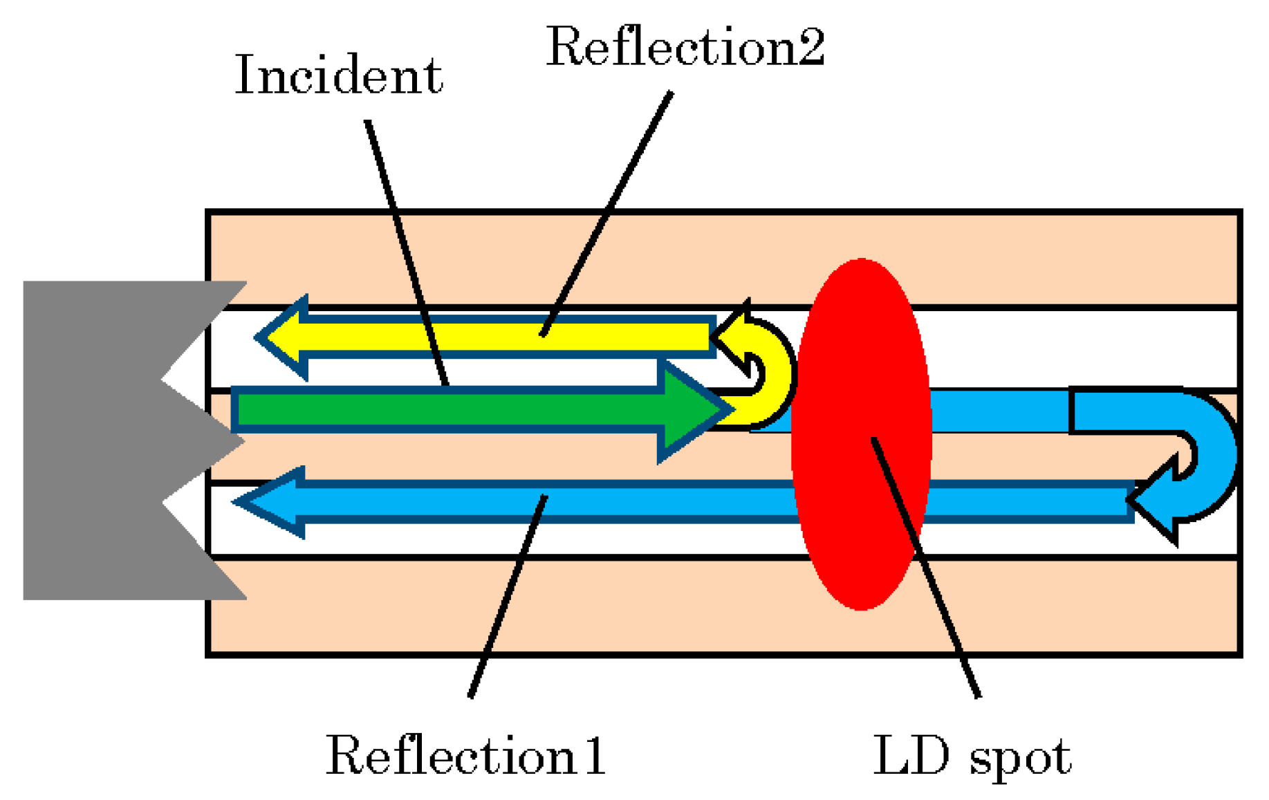
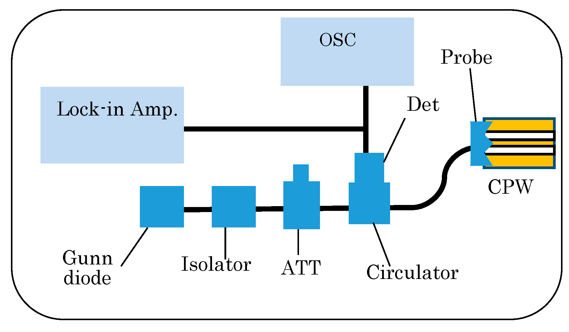
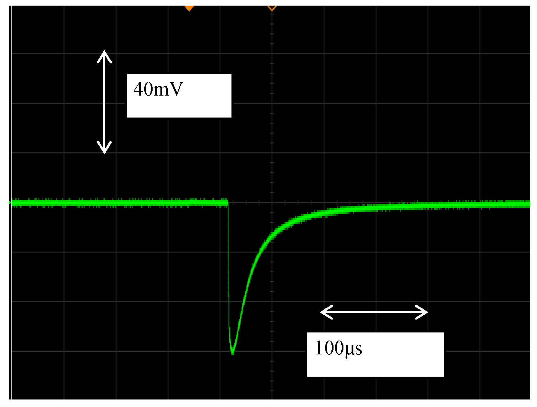
2.1. Principle of Measurement

Figure 1 shows an MMW propagation model on the CPW fabricated using an Si substrate. The incident MMW from the contact probe on the left-hand side propagates to the right, and is reflected at the right-side edge of the CPW. When a pulsed light (905 nm) from the laser diode (LD) is irradiated at a part of the CPW, a temporal electrical short is created, which works as a reflector. Then, a part of the incident MMW is reflected by the optical short. However, the reflectance of the optical short is very small in this stage; thus, a large amount of MMW transmits and is then reflected at the right-side edge. In this case, interference between the reflected MMWs from the optical short and that reflected from the right-side edge is observed. If we move the irradiation position laterally, the length of the propagation path difference between them can be changed. The intensity of the interference changes periodically according to the waveguide’s wavelength, which is influenced by the refractive index of the substrate and upper air. If we introduce an LC material into the CPW, the wavelength in the waveguide is modulated by the refractive index of the LC material. Furthermore, if we focus on the intensity peak, it gradually decreases with the increasing propagation length of the reflected MMW, which is related to the loss of the substrate and the upper introduced material. Here, a bare CPW fabricated using an Si substrate was used for the experiment to check the validity of this method. In this case, the refractive index and loss of the Si substrate could be evaluated, because the loss is negligible for the upper air, while its refractive index is unity.
Figure 2 shows a schematic diagram of our measurement system. A Gunn diode oscillator (40 GHz) was used as the MMW source and it was fed to the CPW by the contact probe through an isolator, attenuator, and circulator in turn. The reflected MMW from the CPW was guided to a diode detector through the isolator, and a temporal change in the interference intensity was observed using an oscilloscope. The synchronized intensity change referring to the LD pulse train was monitored using a lock-in amplifier.

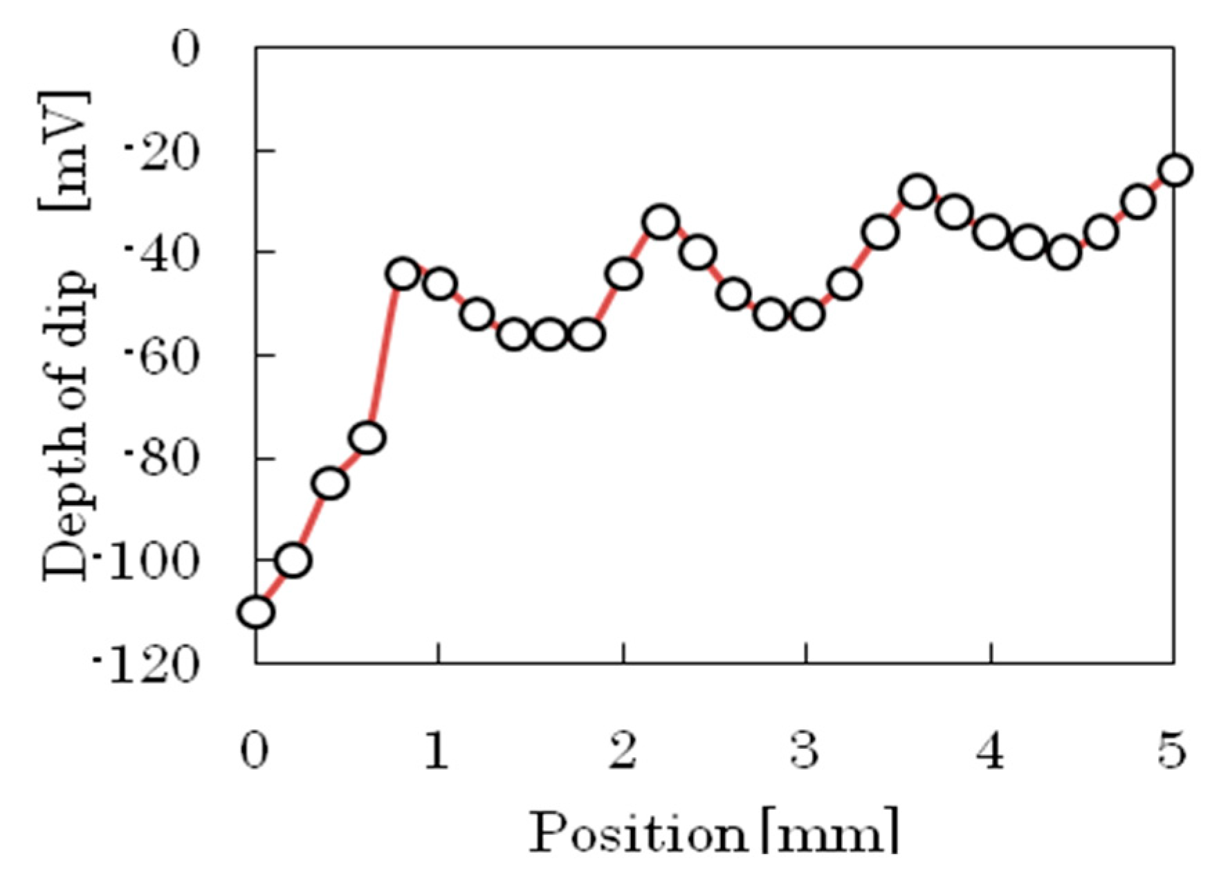
2.2. Evaluation of Refractive Index and Absorption Coefficient

Figure 3 shows a typical measured time waveform appearing on the oscilloscope. The periodic dip waves were observed according to the LD light pulse irradiation and one of them is shown, where the LD pulse repetition is defined at 100 Hz by the external oscillator. The interference between the MMWs reflected at the optical short and at the right-sideend caused a dipping-waveform intensity response. It was observed that the interference disappeared about 50 μs after the LD pulse irradiation, which was determined by the diffusion and recombination phenomena of photo carriers because the laser pulse width was much shorter (100 ns) than the response time. The baseline of the response waveform shows the MMW intensity level reflected from the right-side edge of the CPW without the LD light irradiation, which is much larger than the dip depth of the time waveform. This situation is difficult to understand from Figure 3, because the wave is observed under the alternating current (AC) coupling mode. The interference wave generally became smaller than the baseline level, and only the dipping wave form was observed. This was probably caused by some absorption phenomenon due to the optical short, which may work not only as a reflector, but also as an absorber of MMW.
The interference effect appeared at the dipping part in the time waveform; thus, we measured the depth change of the dipping wave as a function of the LD light irradiation position, as shown in Figure 4. It was observed that the depth changed periodically according to the position, which is caused by the MMW propagation path length change between the interference MMWs. The period corresponds to the waveguide wavelength; thus, the refractive index of the waveguide material can be determined from the wavelength. The absorption coefficient can be determined from the decreasing rate of the dipping depth as a function of the propagation length, if we assume the simple Lambert–Beer law for the dip depth dependency.
The interference phenomena could be clearly observed only aroundthe shorter distance position from the contact probe, and it became difficult to observe when the propagation length of the reflected MMW by the optical short became longer. This was probably caused by the significant intensity difference between the interference waves, where the reflected MMW by the optical short was much smaller than that reflected from the right-side end. The reflectance of the optical short must be increased to improve the measurement accuracy by optimizing the CPW, wavelength of the LD, and so on.
Table 1 presents the evaluation results of the refractive index and absorption coefficient of the Si substrate using the measurement data in Figure 4. The waveguide wavelength can be directly measured from the periodicity in Figure 4, and the effective refractive index was calculated in comparison with the vacuum wavelength. The permittivity was calculated from the refractive index, because the refractive index is simply related to relative permittivity in high-frequency regions like MMW. The obtained permittivity was almost the same as that with the mean value of an intrinsic Si semiconductor and air, because the propagating MMW experienced permittivity similarly for both substrate and air. On the other hand, the absorption coefficient was larger than the commonly known value for Si semiconductors. There is almost no absorption by air; thus, the absorption of the CPW comes from the Si substrate. Although the reason for the discrepancy is not clear at this stage, a precise interference model of the reflection MMWs should be introduced to determine the loss parameter instead of the simple calculation model used here. Although some challenges still remain for measuring the LC materials, since a cell structure must be introduced onto the Si substrate surface, the potential of the optical short working as a noncontact movable reflector was verified in the experiment.

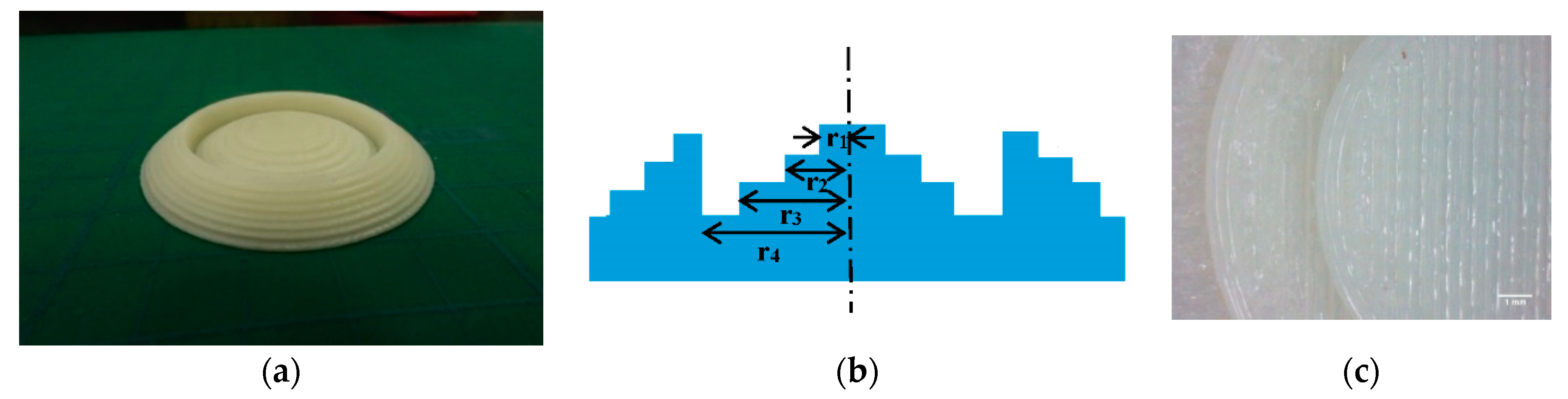
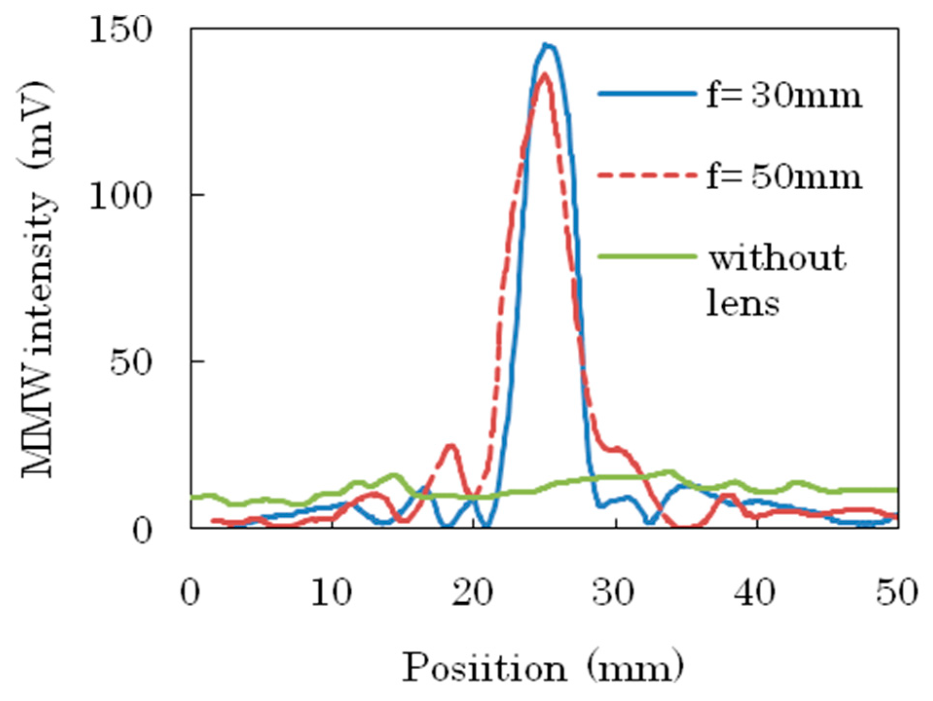
3. Millimeter Wave Fresnel Lens Fabricated Using 3D Printer

One LC device application style in the MMW region involves scaling up some actual LC devices used in the optics region, such as lenses and prisms; these are classified asquasi-optical devices. Although this device type generally has a simple device structure for attaining a specific functionality, the device size increases according to the wavelength. The Fresnel lens is an important and common component for controlling MMW propagation like an optical beam. If we introduce LC materials to the passive components, variable and/or switchable lenses can be obtained. However, simple scale up of the LC cell structure, which is utilized normally for optical devices, causes fatal degradation of the response speed because the wavelength of MMW is significantly longer than that of the optics region. Thus, we tried introducing a PDLC structure to attain an extremely thick LC layer using porous polymer materials [33,34,35]. In this section, we show a fabrication method of a mm-size device structure using a 3D printer, which will be used as a substrate of the MMW LC device combined with porous polymers to introduce the PDLC structure in our next work.

3.1. Design of Fresnel Lens Substrate

Figure 5a shows a typical Fresnel lens fabricated using a 3D printer in this study, where a period of the Fresnel zone was divided by eight steps. It is not easy to attain eight or more step divisions if we use the mechanical milling method because the size of the milling cutter is limited [35]. However, the 3D printer has sufficient precision to attain the MMW Fresnel lens, which has a larger number of divided steps. As mentioned above, the lens surface was approximated by the discrete steps, and the radius was suitably designed for MMW applications using Equation(1), and Figure 5b shows an example of a cross-sectional structure for P = 4 [54]. Here, m is the zone number of the Fresnel lens, P is the dividing number of steps for each Fresnel zone period, f is the focal length, and λ is the wavelength of the MMW. If the dividing number of steps P increases, a higher diffraction efficiency can be obtained. However, a sufficiently high efficiency can be obtained even with values of P between 4 and 8. The optimal depth of a step for maximal diffraction efficiency can be designed using Equation (2), which is determined from the refractive index difference between the substrate and the cavity space. This fact means that the step depth must increase if we introduce the LC material to the cavity, because unity in the equation should be changed to the refractive index of the LC material. The processing accuracy of a domestic 3D printer is enough for the fabrication of an MMW Fresnel lens. Although we can see some roughness on the surface caused by the lamination process of the 3D printer, as shown in Figure 5c, it is not a serious problem for MMW applications, because excellent MMW focusing properties were confirmed from the measurement results of lens properties.
r m = 2 m f λ P + ( m λ P ) 2 ;
d = λ P ( n 1 ) .
Figure 6 shows the measurement data of the MMW focusing properties of the fabricated Fresnel lenses, whose focal lengths were 30 mm and 50 mm, with a diameter of about 50 mm. The 70 GHz MMW generated by the Gunn diode oscillator was radiated from a circular horn antenna, and it was incident normally to the Fresnel lens about 350 mm awayfrom the antenna. The spatial distribution of the MMW intensity in a focal plane of the lens was measured by scanning a diode detector set on a linear stage. It was observed that excellent focusing properties could be obtained in comparison with the background MMW intensity level even though there were only two periods of Fresnel structure. The measured diameter of the focusing spot of about 5 mm is close to the diffraction limit, if we consider that the wavelength of the MMW is 4.3 mm. It is also observed that the spot diameter of the lens with a focal length of 30 mm is a little smaller than that of the lens with a focal length of 50 mm. The difference is reasonable if we consider the difference between their numerical apertures.

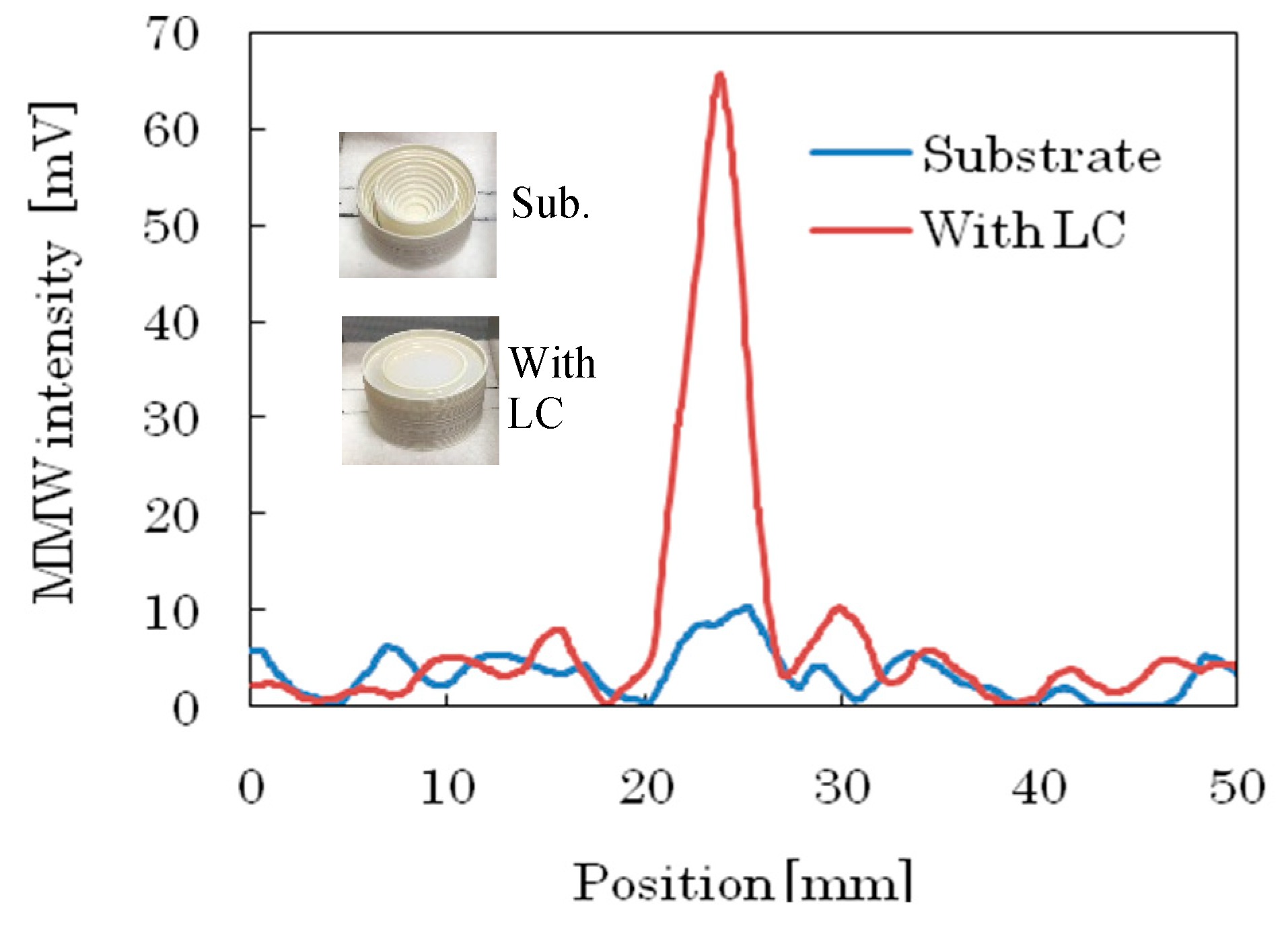
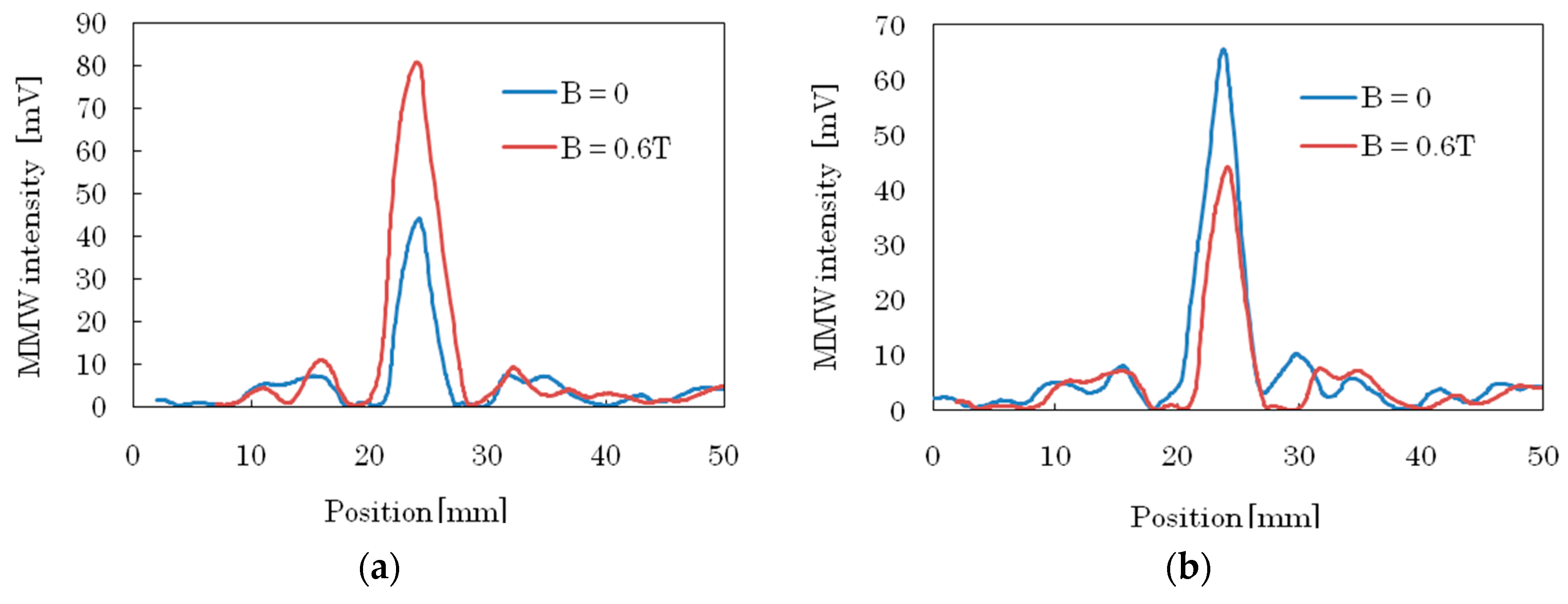
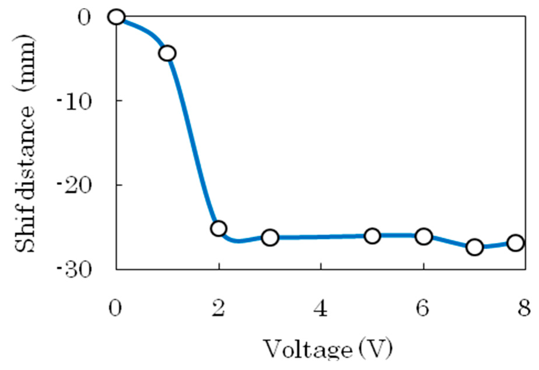
3.2. Magnetic Field Tunable Properties of LC Composite Fresnel Lens

Figure 7 shows the MMW focusing properties of the combined LC Fresnel lens. The inset figures show the fabricated Fresnel lens substrate used in a demonstration of the MMW LC Fresnel lens. The substrate had a concave structure, and the LC material was introduced into the cavity. The diverging property of the concave lens substrate without the LC material is difficult to confirm from the spatial distribution measurement of the MMW intensity; however, it is evident that a good focusing property appeared after introducing the LC material. The combined lens becomes a conversing lens, because the refractive index of the LC materials is larger than that of the plastic material used for the 3D printer filaments.
The combined LC Fresnel lens was set at the center of the pole pieces of the electric magnet system, which was aligned horizontally. In our experiment, the horizontally launched MMW from the horn antenna was reflected vertically by a metal-plate reflector set at an angle of 45°, and the MMW was incident on the Fresnel lens normally from the bottom surface. When a magnetic field is applied to the LC cell, the LC molecules align parallel to the magnetic field because of the anisotropic magnetic response of the LC molecules. If the electric field of the incident MMW is parallel to the applied magnetic field, the MMWs see a large refractive index according to ne, and, if the relationship becomes perpendicular, the refractive index becomes small, corresponding to no.
Figure 8 shows the measurement results of the MMW focusing properties when a magnetic field was applied (a) parallel and (b) perpendicular to the electric field of the MMW. At the initial state, the LC molecular alignment directions were random and, subsequently, the MMW experienced the mean refractive index value between ne and no. When a magnetic field was applied parallel to the MMW electric field, the refractive index of the LC layer increased, i.e., the refractive index difference between the substrate and LC layer increased. Then, the diffraction efficiency of the combined lens tended to increase, as shown in Figure 8a. On the other hand, the focusing intensity decreased when the magnetic field was applied perpendicular to the electric field of the MMW. There was a difference in the MMW intensity at B = 0 between the measurement results in Figure 8a,b. The measurement condition between them was probably a little different because we had to rotate the polarization direction of the MMW oscillator and detector system by 90°. Although the initial intensity at B = 0 had some dispersion between the measurements, the complementary change of the MMW intensity according to the polarization direction was always clear. These results suggest that the refractive index of the 3D printer filament has a smaller refractive index than no of the LC material. If we evaluate the refractive index of the filament material from the measurement data of the diffraction efficiency properties as a function of the step depth, a refractive index of about 1.6 is evaluated from the optimal depth value. This is consistent with the previously measured data of the refractive indices of 5CB in the MMW region, which are 1.71 and 1.62 for ne and no, respectively [8].

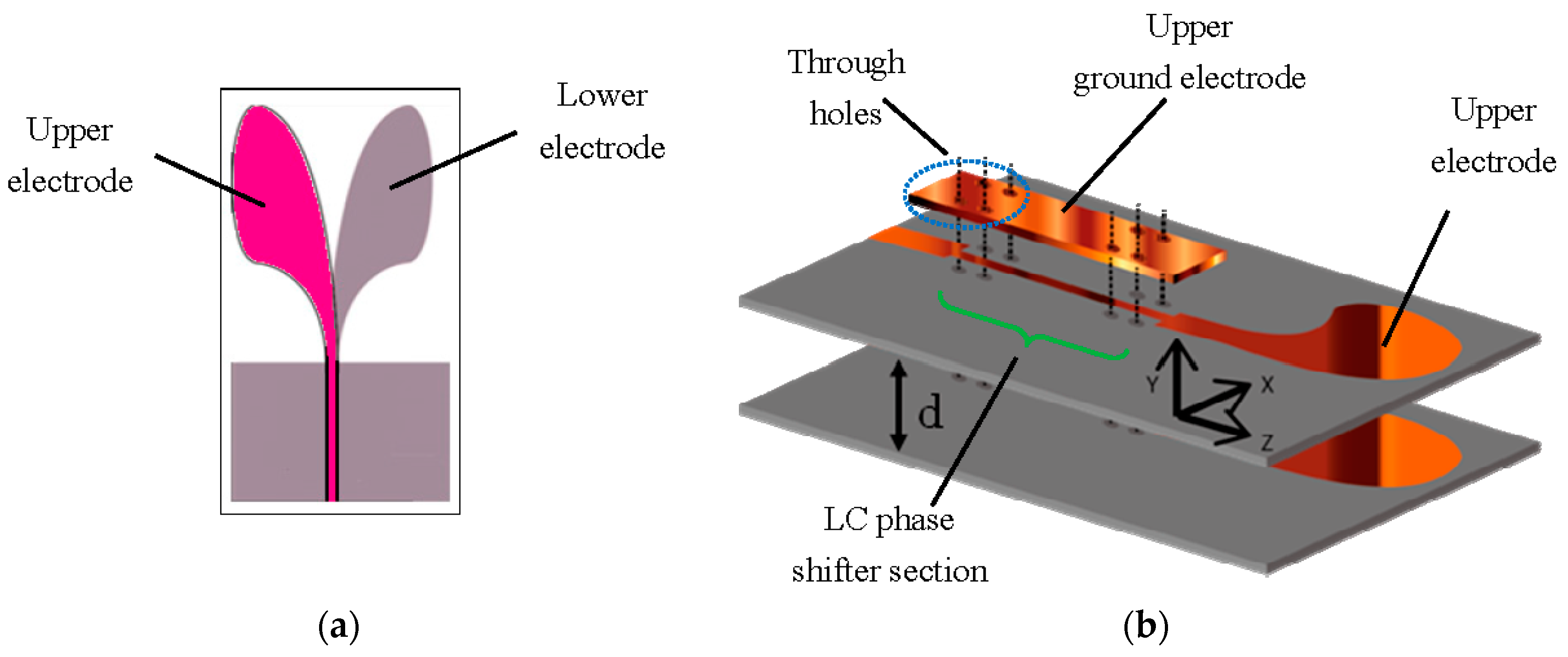
4. Microstrip-Line-Type Liquid Crystal Phase Shifter

There are generally two approaches to develop LC MMW devices. One uses a quasi-optical device, which was described in Section 3. In this section, we describe another approach, which can be attained by integrating LC materials into high-frequency electric circuits. In particular, the integration of LCs with planar-type circuits is popular because it can have a thin planar cell structure, which allows a similar fabrication technology to a flat-panel display. We investigated the LC phase shifter by adopting an excellent planar-type waveguide (microstrip line), which is a very common and reliable waveguide. However, it is not useful to introduce LC materials onto the substrate to control the MMW propagation because the electromagnetic wave propagates inside the dielectric substrate. Thus, we developed a novel conversion circuit to allow integration of the LC material onto the microstrip line [49,50,51]. There is another advantage of the planar-type LC phase shifter, whereby it is easy to expand its functionality to add other necessary parts onto the same substrate as the LC material. In this study, we integrated a planar-type antenna with the LC phase shifter to investigate the minimal twin antenna array.

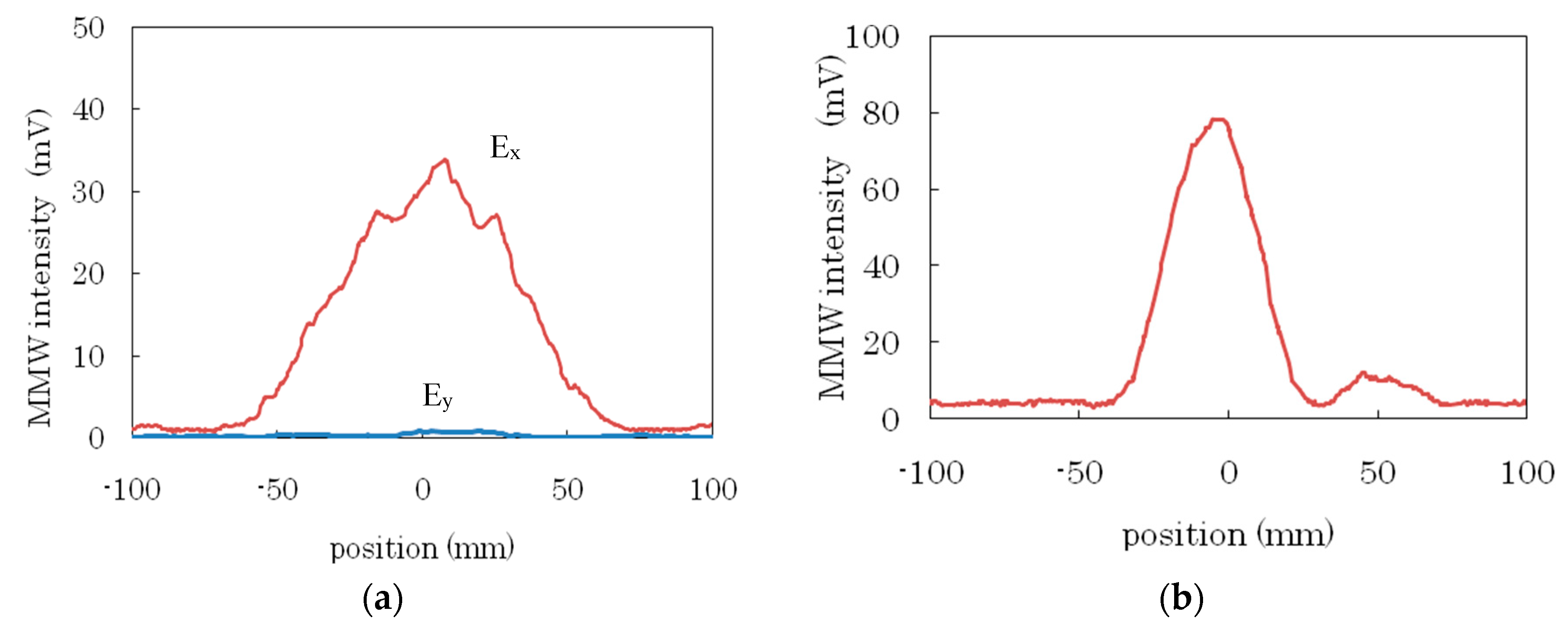
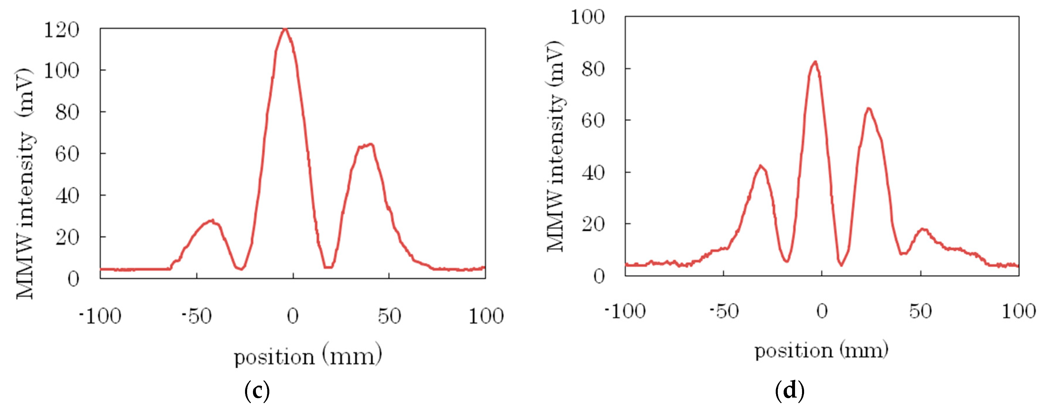
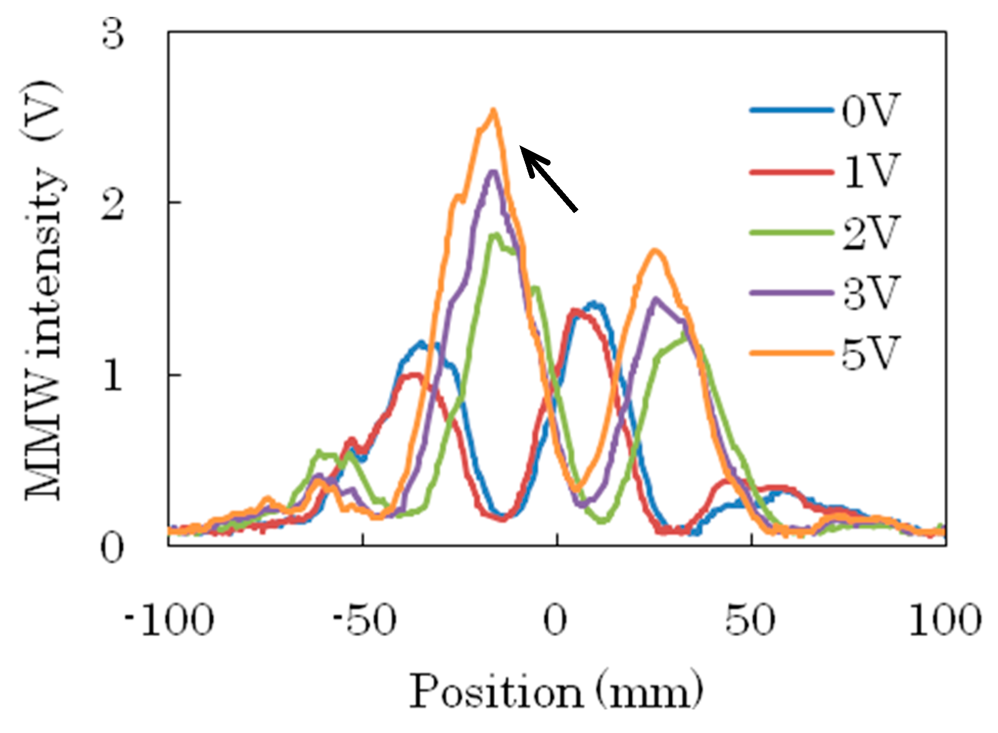
Basic Performance of Antenna Array

Figure 9 shows a schematic diagram of a twin module array consisting of an LC phase shifter and an antenna. One of the antenna electrodes was on the upper surface, which was connected to a signal electrode of the microstrip line; the other was on the bottom surface, which was connected to the ground electrode. Both electrodes were aligned symmetrically, as shown in Figure 9a. Figure 9b shows a configuration of the twin antenna array, in which the units were aligned vertically. A metal plate was mounted on a part of the dielectric substrate of each microstrip line to construct the LC cell structure using a thin insulating spacer. The LC material was introduced to the cell cavity to construct the LC phase shifter. Each end of the upper metal plate had four through-holes to connect with the ground electrode on the lower surface of the microstrip line. This worked as the conversion circuit, which could switch the MMW propagation path between the lower dielectric substrate and the upper LC layer; then, the LC material could modulate the propagation of MMW. The conversion circuit allowed the introduction of the LC material onto the surface of the substrate to develop an LC phase shifterusing a microstrip line. The planar-type antenna was also easily introduced onto the same substrate, as shown in Figure 9b, in which only the upper electrode of the planar antenna appeared.
Initially, the spatial distribution properties of the MMW intensity radiating from the planar antenna were measured along the direction perpendicular to the substrate (y-direction), as shown in Figure 10a. The MMW (50GHz) generated by the Gunn diode oscillator was fed to the left end of the planar antenna through the end launch connector. The spatial distribution of the radiated MMW intensity was measured by a diode detector mounted on the xy stage, which was set at a distance of 150 mm from the antenna. A short rectangular waveguide was mounted on the incident window of the diode detector; thus, it could only detect the MMW polarization direction parallel to the short arm of the waveguide aperture. It can be seen that the radiating MMW was strongly polarized horizontally (x-direction), because the vertical component (Ey) was negligible. This result is reasonable if we consider that the electrodes of the antenna were aligned in the substrate plane. A symmetric distribution profile appeared along the direction perpendicular to the substrate plane, as shown in Figure 10a. Although we observed some asymmetric distribution along the direction parallel to the substrate, it was clear that the stack of the antennas along the y-direction was effective in checking the performance of the antenna array.
Two units combining the LC phase shifter and planar antenna were aligned as their substrates became parallel to each other, as shown in Figure 9b. The radiated MMW intensity distribution properties of the twin antenna array were measured by changing the separation distance between them at 10 mm, 20 mm, and 30 mm, as shown in Figure 10b–d, respectively. It was observed that the MMW distribution profile became narrower and the intensity peak increased upon constructing the array. The main MMW beam tended to be narrower with increasing distance between the antennas; however, it was also observed that the side lobe tended to increase for the longer distance.
Figure 11 shows the MMW intensity distribution change of the twin array system when a voltage was applied to the LC phase shifter, in which the distance between the antennas was set at 20 mm. Three peaks appeared under the experimental conditions, and slight asymmetry existed without voltage because of some differences between the two units. When voltage was applied to the LC phase shifter at the left-hand side (minus position) in the figure, the wave front was deformed to the left side and it was seen that the main beam shifted to the left side. The maximal shift distance was about 30 mm, which was 150 mm away from the antenna. This change corresponds to anangle change of about 12°; the ±12° beam steering could be achieved by alternatively driving each 40-mm-long LC phase shifter. Since three peaks appeared in the experiment, we focused on the central peak. It was possible to follow the position of each peak, because the position changed continuously as a function of the applied voltage, even if it was quite nonlinear.
The position change of the central beam as a function of the applied voltage is shown in Figure 12. A large change occurs between 1 and 2 V before tending to saturate, which is related to the typical LC molecular orientation change in the homogeneously aligned LC cell. Although the driving voltage is very small, up to only a few volts, a precise voltage control around the threshold is essential for precise beam steering. It is also obvious that the position change accompanied a large intensity change. This may cause difficulties in actual usage; thus, a specific driving scheme will be necessary.

5. Conclusions

In this study, we described some recent investigations intothe application of LC materials in the MMW frequency region. There is insufficient knowledge about specialized LC materials for MMW application; thus, the development of efficient measurement methods for LC materials is essential for exploring excellent materials in this frequency region. We successively investigated the issue using various types of waveguides, and a planar waveguide (CPW) was introduced to significantly decrease the size of the test sample. However, the metal plate inserted into the LC cell, which worked as a moving reflector, destroyed the alignment layer of the LC molecules in one measurement. To overcome this problem, an optical short was introduced using a semiconductor substrate for the microstrip line. An optical short, which can work as a reflection boundary of MMW, was confirmed by irradiating an intense laser pulse to create a high-density photo-carrier domain. The reflection boundary could easily be moved by changing the irradiation position of the laser light. The refractive index and absorption coefficient of the substrate material could be successfully evaluated from the periodicity and attenuation of the MMW peak intensity as a function of the laser light irradiation position.
There are two approaches to develop LC MMW devices. The first involves scaling up an LC optical device according to the increase in the wavelength; this is called aquasi-optical device. A Fresnel lens is a typical quasi-optical device used in the MMW region, and it becomes tunable if we introduce LC materials into the lens. The device structure is generally simple and easy to design following almost the same method used with optical devices. In this study, we demonstrated the basic performance of a Fresnel lens fabricated using a 3D printer. The filament material of the printer had relatively low loss properties in the MMW region, and the fabricated Fresnel lenses exhibited excellent focusing properties, even if some roughness was caused by the laminating process. The LC material was combined with a concave Fresnel lens substrate fabricated by the 3D printer to develop an LC Fresnel lens. A magnetic field was applied to control the LC molecular orientation, and the complementary focusing MMW intensity change was observed upon changing the magnetic field direction.
Another approach to develop LC MMW devices involves integrating LC materials with high-frequency electric circuits. If we adopt a planar wave guide, a thinner sandwich cell structure can be used for MMW LC devices. This is the biggest advantage in comparison with the quasi-optical approach. In this study, we demonstrated an LC phase shifter by combining LC materials with a microstrip line, which is a very common and excellent planar-type waveguide used to construct high-frequency integration circuits. We demonstrated the basic performance of the minimal twin antenna array system, which was attained upon combination with LC phase shifters. It was confirmed that the radiated MMW beam became narrower by the arrays, and the peak intensity tended to increase. A beam-steering angle of about ±12° could be obtained by driving each LC phase shifter with a low voltage; however, the changing property was extremely nonlinear as a function of the applied voltage because of the LC molecular orientation phenomena in the homogeneously aligned LC cell. This approach is advantageous in terms of response speed, because the thinner LC layer is beneficial. However, some other components, such as a power divider, LC driver circuit, and antenna, must be integrated with the LC phase shifter to attain specific functionality.
On the other hand, the device structure in the quasi-optical device is simple for achieving specific functionality. However, a thousand-fold increase of the LC layer is necessary to attain a similar operation to optical devices. A simple increase in the normal cell structure causes a fatal degradation of response speed; thus, we tried adopting the PDLC structure using the porous PMMA material to construct the MMW Fresnel lens. However, the driving method for extremely thick LC still remains a problem that must be solved to develop this type of actual MMW LC device. For any approach, the final device performance is governed by the LC material properties. Exploring novel LC materials for MMW application is still an important issue. Currently, LC materials are not optimized for MMW and/or THz application; thus, we believe that the device performance can be greatly improved when specialized LC materials appear. Further, investigation of the basic performance of any type of LC device is important for the actual application of LC materials to the MMW region.

Funding

Some of the experiments related to optical short were performed using the measurement equipment provided by the SCOPE project (135002002), Ministry of Internal Affairs and Communications, Japan. The study about quasi-optical LC MMW devices was partly supported by the Japan Society for the Promotion of Science (JSPS) Grant in Aid for Scientific Research (C) 15K06025. The study about electro optic and/or magneto optic phenomena of LC materials was partly supported by the JSPS Grant in Aid for Scientific Research (C) 18K04928.

Acknowledgments

The authors appreciate the successive support by Yurikogyo Co. Ltd., Japan. The authors appreciate the helpful discussion about optical short by Professor J. Bae in Nagoya Institute Technology, Japan.

Conflicts of Interest

The authors declare no conflicts of interest.

References

  1. Vicari, L. Optical Application of Liquid Crystals, 1st ed.; CRC Press: Boca Raton, FL, USA, 2003. [Google Scholar]
  2. Larsen, T.T.; Bjarklev, A.; Hermann, D.S.; Broeng, J. Optical devices based on liquid crystal photonics bandgap filter. Opt. Express 2003, 11, 2589–2596. [Google Scholar] [CrossRef]
  3. Bitou, Y. Digital phase-shift interferometer with an electrically addressed liquid crystal spatial light modulator. Opt. Lett. 2003, 28, 1576–1578. [Google Scholar] [CrossRef] [PubMed]
  4. Honma, M.; Horiuchi, T.; Nose, T. Oblique extraction of polarized light from light-emitting liquid crystal cells doped with a fluorescent dye. Jpn. J. Appl. Phys. 2013, 52, 070205. [Google Scholar] [CrossRef]
  5. Nose, T.; Kamata, K.; Takeuchi, T.; Okano, K.; Fujita, N.; Muraguchi, H.; Ozaki, N.; Honma, M.; Ito, R. Determination of birefringence and slow axis distribution using an interferometric measurement system with liquid crystal phase shifter. Appl. Opt. 2014, 53, 7230–7235. [Google Scholar] [CrossRef]
  6. Yang, D.K.; Wu, S.T. Fundamentals of Liquid Crystal Devices, 2nd ed.; Wiley: Hoboken, NJ, USA, 2014. [Google Scholar]
  7. Wang, L.; Dong, H.; Li, Y.; Xue, C.; Sun, L.; Yan, C.; Li, Q. Reversible near infrared light directed reflection in a self-organized helical superstructure loaded with upconversion nanoparticles. JACS 2014, 136, 4480–4483. [Google Scholar] [CrossRef] [PubMed]
  8. Wang, L.; Dong, H.; Li, Y.; Liu, R.; Wang, Y.; Bisoyi, H.K.; Sun, L.; Yan, C.; Li, Q. Luminescence-driven reversible handedness inversion of self-organized helical superstructures enabled by a novel near infrared light nanotransducer. Adv. Mater. 2015, 27, 2065–2069. [Google Scholar] [CrossRef] [PubMed]
  9. Buchnev, O.; Podoliak, N.; Kaczmarck, M.; Zheludev, N.I.; Fedotov, V.A. Electrically controlled nanostructured metasurface loaded with liquid crystal: toward multifunctional photonic switch. Adv. Opt. Mater. 2015, 3, 674–679. [Google Scholar] [CrossRef]
  10. Wang, L.; Li, Q. Stimuli-directing directing self-organized 3D liquid crystalline nanostructures: from material design to photonic applications. Adv. Funct. Mater. 2016, 26, 10–28. [Google Scholar] [CrossRef]
  11. Wang, L. Self-activating liquid crystal devices for smart laser projection. Liq. Cryst. 2016, 43, 2062–2078. [Google Scholar] [CrossRef]
  12. Nose, T.; Ishizaka, S.; Okano, K.; Fujita, N.; Murata, J.; Muraguchi, H.; Ozaki, N.; Honma, M.; Ito, R. Differential interference contrast imaging using a pair of twisted nematic cells. Opt. Lett. 2016, 41, 4012–4015. [Google Scholar] [CrossRef]
  13. Honma, M.; Nose, T. Polarization conversion system with liquid crystal geometric-phase-based cylinder lens. Jpn. J. Appl. Phys. 2016, 55, 012202. [Google Scholar] [CrossRef]
  14. Honma, M.; Miura, T.; Nose, T. Liquid-crystal-grating-based optical displacement sensors. Appl. Opt. 2016, 55, 10045–10052. [Google Scholar] [CrossRef] [PubMed]
  15. Wang, L.; Huang, D.; Lam, L.; Cheng, Z. Bowkics: history, advances and application. Liq. Cryst. Today 2017, 26, 85–111. [Google Scholar] [CrossRef]
  16. Wang, L.; Bisoni, H.K.; Zheng, Z.; Gutierrez-Cuevas, K.G.; Singh, G.; Kumar, S.; Bunning, T.J.; Li, Q. Stimuli-directed self-organized chiral superstructures for adaptive windows enabled by mesogen-functionalized grapheme. Mater. Today 2017, 20, 230–236. [Google Scholar] [CrossRef]
  17. Gorkunov, M.V.; Kasyanova, I.V.; Artenov, V.V.; Barnik, M.I.; Geivandov, A.R.; Palto, S.P. Fast surface-plasmon-mediated electro-optics of a liquid rystal on a metal grating. Phys. Rev. Appl. 2017, 8, 054051. [Google Scholar] [CrossRef]
  18. Komar, A.; P-Dominguez, R.; Miroshnichenko, A.; Yu, Y.F.; Kivshar, Y.S.; Kuznetsov, A.I.; Neshev, D. Dynamic beam switching by liquid crystal tunable dielectric metasurfaces. ACS Photonics 2018, 5, 1742–1748. [Google Scholar] [CrossRef]
  19. Nose, T.; Mizuno, S.S.K.; Bae, J.; Nozokido, T. Refractive index of nematic liquid crystals in the submillimeter wave region. Appl. Opt. 1997, 36, 6383–6387. [Google Scholar] [CrossRef]
  20. Lim, K.C.; Margerum, J.D. Liquid-crystal optical propertiesand applications in the millimeter-wave range. Proc. SPIE 1992, 1815, 99–103. [Google Scholar]
  21. Lackner, A.M.; Lim, K.C.; Margerum, J.D.; Sherman, E. Microtubule particle dispersion in liquid crystal hosts. Liq. Cryst. 1993, 14, 351–359. [Google Scholar] [CrossRef]
  22. Lim, K.C.; Margerum, J.D.; Lackner, A.M.; Sherman, E.; Ho, M.-S.; Fung, B.M.; Genetti, W.B.; Grady, B.P. Aliquid crystal based polymer for applications in MMW modulationdevices. Mol. Cryst. Liq. Cryst. 1997, 302, 187–197. [Google Scholar] [CrossRef]
  23. Kamoda, H.; Kuki, T.; Fujikake, H.; Nomoto, T. Measurementof microwave dielectric properties of liquid crystal usingcoaxial line. Trans. IEICE C 2002, J85, 776–777. [Google Scholar]
  24. Kamei, T.; Utsumi, Y.; Moritake, H.; Toda, K.; Suzuki, H. Dielectric properties measurement of nematic liquid crystalat 10 kHz–40 GHz and its application for variable delay line. Trans. IEICE C 2002, J85, 1149–1158. [Google Scholar]
  25. Nose, T.; Honma, M.; Nozokido, T.; Mizuno, K. Determinationof the insertion loss and refractive index anisotropy innematic liquid crystal materials using a V-band waveguidetransmission cell. Mol. Cryst. Liq. Cryst. 2004, 409, 199–207. [Google Scholar] [CrossRef]
  26. Nose, T.; Honma, M.; Nozokido, T.; Mizuno, K. Simple method for the determination of refractive indices and loss parameters for liquid-crystal materials in the millimeter-wave region. Appl. Opt. 2005, 44, 1150–1155. [Google Scholar] [CrossRef] [PubMed]
  27. Ito, R.; Yanagihara, S.; Ito, K.; Watanabe, T.; Nose, T.; Honma, M. Basic performance of refractive index measurement method for LC materials in super high frequency region by using coplanar wave guide. Mol. Cryst. Liq. Cryst. 2011, 543, 92–100. [Google Scholar] [CrossRef]
  28. Vogel, T.; Dodel, G.; Holzhauer, E.; Salzmann, H.; Theurer, A. High-speed switching of far-infrared radiation by photoionization in a semiconductor. Appl. Opt. 1992, 31, 329–337. [Google Scholar] [CrossRef] [PubMed]
  29. Nozokido, T.; Minamide, H.; Mizuno, K. Modulation of submillimeter wave radiation by laser-produced free carriers in semiconductor. IEICE Trans. Electron. C 1997, 6, 259–266. (In Japanese) [Google Scholar] [CrossRef]
  30. Tanaka, M.; Sato, S. Focusing properties of liquid crystal lens cells with stacked-layered structure in the millimeter-wave region. IEEE Microw. Wirel. Compon. Lett. 2002, 12, 163–165. [Google Scholar] [CrossRef]
  31. Kamoda, H.; Kuki, T.; Fujikake, H.; Nomoto, T. Millimeter-wave beam former using liquid crystal. In Proceedings of the 34th European Microwave Conference, Amsterdam, The Netherlands, 12–14 October 2004; pp. 1141–1144. [Google Scholar]
  32. Nozokido, T.; Maeda, S.; Okada, H.; Nose, T.; Murai, T. A millimeter-wave quasi-optical grid phase shifter using liquid crystal. IEICE Electron. Express 2010, 7, 67–72. [Google Scholar] [CrossRef] [Green Version]
  33. Nose, T.; Ito, T.; Watanabe, T.; Ito, K.; Yanagihara, S.; Ito, R.; Honma, M. Preparation of porous polymer materials for bulky liquid crystal devices. Proc. SPIE 2012, 8279. [Google Scholar] [CrossRef]
  34. Ohno, S.; Toshima, N.; Honma, R.I.M.; Nose, T. Modified microscopic structure and its LC molecular orientation effects in the stretched porous PMMA films. In Proceedings of the 21st International Display Workshops 2014 (IDW’14), Niigata, Japan, 3–5 December 2014; pp. 129–130, (Nagoya, Japan). [Google Scholar]
  35. Nose, T.; Ohno, S.; Masaka, M.; Ito, K.; Ito, R.; Honma, M. Basic performance of a liquid crystal millimeter wave Fresnel lens fabricated using machinable porous polymethylmethacrylate materials. Mol. Cryst. Liq. Cryst. 2017, 647, 341–350. [Google Scholar] [CrossRef]
  36. Lim, K.C.; Margerum, J.D.; Lackner, A.M.; Miller, L.J.; Sherman, E.; Smith, W.H., Jr. Liquid crystal birefringence for millimeter wave radar. Liq. Cryst. 1993, 14, 327–337. [Google Scholar] [CrossRef]
  37. Lim, K.C.; Margerum, J.D.; Lackner, A.M. Liquid crystal millimeter wave electronic phase shifter. Appl. Phys. Lett. 1993, 62, 1065–1067. [Google Scholar] [CrossRef]
  38. Strunck, S.; Karabey, O.H.; Gaebler, A.; Jakoby, R. Reconfigurable waveguide polariser based on liquid crystal for continuous tuning of linear polarization. Electron. Lett. 2012, 48, 441–443. [Google Scholar] [CrossRef]
  39. Dolfi, D.; Labeyrie, M.; Joffre, P.; Huignard, J.P. Liquid crystal microwave phase shifter. Electron. Lett. 1993, 29, 926–927. [Google Scholar] [CrossRef]
  40. Guerin, F.; Chappe, J.M.; Joffre, P.; Dolfi, D. Modeling, synthesis and characterization of a millimeter-wave multilayer microstrip liquid crystal phase shifter. Jpn. J. Appl. Phys. 1997, 36, 4409–44413. [Google Scholar] [CrossRef]
  41. Kuki, T.; Fujikake, H.; Nomoto, T.; Utsumi, Y. Design of a microwave variable delay line using liquid crystal, and a study of its insertion loss. IEICE Trans. C 2001, J84, 90–96. (In Japanese) [Google Scholar] [CrossRef]
  42. Kuki, T.; Fjikake, H.; Kamoda, H.; Nomoto, T. Microwave variable delay line using a membrane impregnated with liquid crystal. In Proceedings of the 2002 IEEE MTT-S International Microwave Symposium Digest, Seattle, WA, USA, 2–7 June 2002; pp. 363–365. [Google Scholar]
  43. Splingart, B.; Tentillier, N.; Huret, F.; Legrand, C. Liquid crystals application to R. F. and microwave tunable components. Mol. Cryst. Liq. Cryst. 2001, 368, 183–190. [Google Scholar] [CrossRef]
  44. Weil, C.; Luessem, G.; Jakoby, R. Tunable inverted-microstrip phase shifter device using nematic liquid crystals. In Proceedings of the 2002 IEEE MTT-S International Microwave Symposium Digest, Seattle, WA, USA, 2–7 June 2002; pp. 367–370. [Google Scholar]
  45. Karabey, O.H.; Bildik, S.; Strunck, S.; Gaebler, A.; Jakoby, R. Continuously polarisation reconfigurable antenna element by using liquid crystal based tunable coupled line. Electron. Lett. 2012, 48, 141–143. [Google Scholar] [CrossRef]
  46. Garbvskiy, Y.; Zagoridnii, V.; Krivosik, P.; Lovejoy, J.; Camley, R.E.; Celinski, Z.; Glushchenko, A.; Dziaduszek, J.; Dabroeski, R. Liquid crystal phase shifter at millimeter wave frequencies. J. Appl. Phys. 2012, 111, 054504. [Google Scholar] [CrossRef]
  47. Ito, R.; Kawakami, T.; Ito, Y.; Sasamori, T.; Isota, Y.; Honma, M.; Nose, T. Fundamental properties of novel design microstrip line type of liquid crystal phase shifter in microwave region. Jpn. J. Appl. Phys. 2012, 51, 044104-1–044104-5. [Google Scholar] [CrossRef]
  48. Nose, T.; Chien, L.; Catanescu, O.; Golvin, A.; Ito, Y.; Sasamori, T.; Isota, Y.; Ito, R.; Honma, M. Improved high-frequency performance of microstrip-line-type liquid crystal phase shifter. Jpn. J. Appl. Phys. 2013, 52, 091701-1–091701-5. [Google Scholar] [CrossRef]
  49. Nose, T.; Ito, Y.; Iisaka, T.; Chien, L.; Catanescu, O.; Golvin, A.; Isota, Y.; Sasamori, T.; Ito, R.; Honma, M. High-frequency performance extending to millimeter-waves in inverted-microstrip-line-type LC phase shifter. Proc. SPIE 2013, 8642, 864206. [Google Scholar]
  50. Nose, T.; Komuro, T.; Sasamori, T.; Isota, Y.; Watanabe, T.; Ito, K.; Ito, R.; Honma, M. Fundamental performance of liquid crystal millimeter-wave phase shifter using negative dielectric anisotropic material. In Proceedings of the 2014 39th International Conference on Infrared, Millimeter, and Terahertz waves (IRMMW-THz), Tucson, AZ, USA, 14–19 September 2014. [Google Scholar]
  51. Nose, T.; Saito, S.; Yanagihara, S.; Honma, M. Molecular orientation effects in the CPW type LC phase shifters for MMW phase shifting. Proc. SPIE 2006, 6135, 6135F. [Google Scholar]
  52. Nose, T.; Yanagihara, S.; Honma, M. Operational mode of millimeter-wave phase shifter using liquid crystal materials with coplanar waveguide. Jpn. J. Appl. Phys. 2007, 46, 1114–1117. [Google Scholar] [CrossRef]
  53. Nose, T.; Yanagihara, S.; Sato, Y.; Ito, R.; Honma, M. Improvement of phase-shifting properties in coplanar waveguide-type liquid crystal millimeter-wave phase shifter by introducing a resonant phenomenon. Jpn. J. Appl. Phys. 2008, 47, 8483–8486. [Google Scholar] [CrossRef]
  54. Wiltse, J.C. Recent developments in Fresnel zone plate antennas at microwave/millimeter wave. Proc. SPIE 1998, 3464, 146–154. [Google Scholar]
Figure 1. Millimeter-wave (MMW) propagation model on the coplanar waveguide (CPW). LD: laser diode.
Applsci 08 02544 g001
Figure 2. Reflection MMW measurement system. ATT: Attenuator.
Applsci 08 02544 g002
Figure 3. Typical measurement waveform appearing according to the irradiation of a laser diode (LD) pulse.
Applsci 08 02544 g003
Figure 4. Dip depth property as a function of propagation length of the MMW reflected by the optical short.
Applsci 08 02544 g004
Figure 5. (a)Appearance of fabricated Fresnel lens; (b) an example of the cross-sectional structure of the Fresnel lens; (c)magnified observation of the lens surface fabricated using a three-dimensional (3D) printer.
Applsci 08 02544 g005
Figure 6. MMW focusing properties of conversing lens.
Applsci 08 02544 g006
Figure 7. MMW focusing properties of the combined liquid-crystal (LC) Fresnel lens.
Applsci 08 02544 g007
Figure 8. Changes in MMW focusing property of the LC composite Fresnel lens upon applying a magnetic field (a) parallel or (b) perpendicular to the electric field of the MMW.
Applsci 08 02544 g008
Figure 9. (a) Antenna electrode pattern, where both electrodes on the upper and lower surfaces are shown at the same time; (b) twin vertical array of antenna modules, which consists of a planar antenna and an LC phase shifter.
Applsci 08 02544 g009
Figure 10. (a) Radiation profile of an antenna along the direction perpendicular to the substrate. Radiation profiles of the twin array of antenna modules, whose distances are (b) 10 mm, (c) 20 mm, and (d) 30 mm.
Applsci 08 02544 g010aApplsci 08 02544 g010b
Figure 11. MMW radiation profile change upon driving an LC phase shifter.
Applsci 08 02544 g011
Figure 12. Position change of the central beam as a function of the LC deriving voltage.
Applsci 08 02544 g012
Table 1. Evaluation results of the Si substrate.
λg (mm)nεrα (mm−1)
Measurement2.772.717.340.079
Reference-3.6130.011

