Article

Influence of Interfacial Intermetallic Growth on the Mechanical Properties of Sn-37Pb Solder Joints under Extreme Temperature Thermal Shock

1
State Key Laboratory of Advanced Welding and Joining, Harbin Institute of Technology, Harbin 150001, China
2
Shanghai Academy of Spaceflight Technology, Shanghai 201109, China
*
Author to whom correspondence should be addressed.
Appl. Sci. 2018, 8(11), 2056; https://doi.org/10.3390/app8112056
Submission received: 25 September 2018 / Revised: 15 October 2018 / Accepted: 22 October 2018 / Published: 25 October 2018
(This article belongs to the Special Issue Selected Papers from the NMJ2018)

Abstract

:
Solder joints in thermally uncontrolled microelectronic assemblies have to be exposed to extreme temperature environments during deep space exploration. In this study, extreme temperature thermal shock test from −196 °C to 150 °C was performed on quad flat package (QFP) assembled with Sn-37Pb solder joints to investigate the evolution and growth behavior of interfacial intermetallic compounds (IMCs) and their effect on the pull strength and fracture behavior of Sn-37Pb solder joints under extreme temperature environment. Both the scallop-type (Cu, Ni)6Sn5 IMCs at the Cu lead side and the needle-type (Ni, Cu)3Sn4 IMCs at the Ni-P layer side changed to plane-type IMCs during extreme temperature thermal shock. A thin layer of Cu3Sn IMCs was formed between the Cu lead and (Cu, Ni)6Sn5 IMC layer after 150 cycles. The growth of the interfacial IMCs at the lead side and the Ni-P layer side was dominated by bulk diffusion and grain-boundary diffusion, respectively. The pull strength was reduced about 31.54% after 300 cycles. With increasing thermal shock cycles, the fracture mechanism changed from ductile fracture to mixed ductile–brittle fracture, which can be attributed to the thickening of the interfacial IMCs, and the stress concentration near the interface caused by interfacial IMC growth.

1. Introduction

During space exploration, thermally uncontrolled microelectronic assemblies have to be exposed to extreme temperature environments with large temperature variations, such as under the condition of Moon (−180 °C to 150 °C), Mars (−140 °C to 20 °C) and Giant Planets (−140 °C to 380 °C) [1]. Solder joints provide mechanical support and electrical connection in microelectronic assemblies, the performance and quality of solder joints are vital to the overall functioning of microelectronic assemblies [2,3].
The formation and growth of intermetallic compounds (IMCs) at interface between the solder and the substrate are inevitable during soldering and processing [4,5]. The evolution and growth of interfacial IMCs significantly affect the mechanical properties and reliability of solder joints due to the intrinsically brittle nature of IMCs [6,7,8]. In our previous study [9], we found that the fast growth of interfacial IMCs in Sn-3Ag-0.5Cu solder joints was responsible for the early formation of cracks at the Sn-3Ag-0.5Cu solder/IMC layer interface under extreme temperature thermal shock from −196 °C to 150 °C, and the growth of interfacial IMCs and crack formation at the IMC layer/solder interface led to the reduction in pull strength of Sn-3Ag-0.5Cu solder joints. Sn-Pb solder alloys are commonly used in deep space application until now [10]. Thus, it is essential to investigate the evolution and growth behavior of interfacial IMCs in Sn-Pb solder joints and their effect on the mechanical properties of Sn-Pb solder joints under extreme temperature environment. However, the correlating research is very limited.
In this study, extreme temperature thermal shock test from −196 °C to 150 °C was conducted on quad flat package (QFP) assemblies to investigate the evolution and growth behavior of interfacial IMCs in Sn-37Pb solder joints under extreme temperature environment. Pull test was adopted to evaluate the pull strength and fracture behavior of Sn-37Pb solder joints. Based on these results, the effect of interfacial IMC growth on the pull strength and fracture behavior of Sn-37Pb solder joints was discussed.

2. Materials and Methods

2.1. Sample Preparation

The test module used in this study was 64 pins QFP with the 0.5 mm pitches. The “L” configured leads were made of copper. An electroless nickel immersion gold (ENIG) surface finish was applied to the substrate pads. The solder paste used in this study was Sn-37 wt.% Pb (DSP 825HF, Qualitek, Shenzhen, China). QFP was assembled on the substrate using a reflow oven (Heller 1706 EXL, Heller, Troy, MI, USA). The peak reflow temperature was 215 °C, and the duration above liquidus (183 °C) was about 60 s. Figure 1 shows the cross section of the samples after reflowing.

2.2. Extreme Temperature Thermal Shock Test

The extreme temperature thermal shock test was conducted on the as-reflowed samples by converting the samples between liquid nitrogen container and constant temperature furnace (WHLL-30BE) for 350 cycles. The maximum and minimum temperatures in extreme temperature thermal shock test were 150 °C and −196 °C, respectively. The temperature ramp rate was higher than 30 °C/min. The dwell times at the maximum and minimum temperatures were both 30 min. After every 50 cycles, five samples were extracted out for microstructure examination and pull test [11].

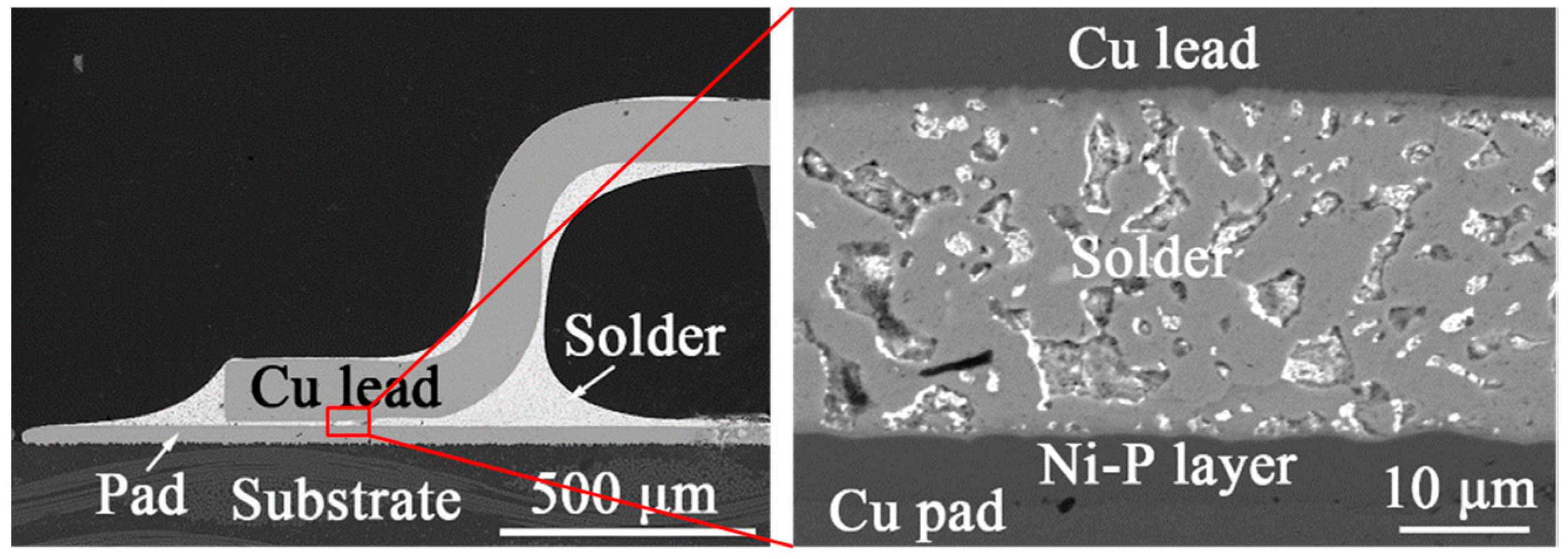
2.3. Microstructure Examination

The as-soldered and thermally shocked samples were divided into two groups. One group of the samples were embedded in epoxy resin. The embedded samples were ground, polished and then etched with a solution of 5 g FeCl3 + 15 mL HCl + 85 mL H2O for 15 s to reveal the interfacial microstructures of solder joints. The interfacial microstructures of the solder joints were observed and the chemical compositions of the interfacial IMCs were quantitatively measured using a scanning electron microscope (SEM, Quanta 200FEG, FEI, Hillsboro, USA) equipped with energy dispersive spectroscopy (EDS). The thickness of the IMC layer was obtained using SEM images showing the interfacial microstructure of the solder joints. The thickness of the IMC layer was calculated using Equation (1):
LIMC = (NIMC/NSEM) × LSEM,
where LIMC is the thickness of the IMC layer, LSEM is the height of the SEM image, and NSEM and NIMC are the number of pixels in the entire SEM image and the IMC layer, respectively. NSEM and NIMC were measured by using Image J V1.8.0 software. For each condition, more than eight SEM images showing the interfacial microstructure of the solder joints were measured to obtain the average value of the IMC layer thickness and to minimize the error.

2.4. Pull Test and Fractography

For the second group of samples, 45° pull test (JIS Z 3198-6) was adopted to evaluate the mechanical property of solder joints. The pull test was conducted at room temperature using a DAGE 4000 pull tester. More than eight leads located at the outer edge of QFPs were pulled for each test condition. After pull test, fracture surfaces of the solder joints were analyzed using SEM and EDS.

3. Results and Discussion

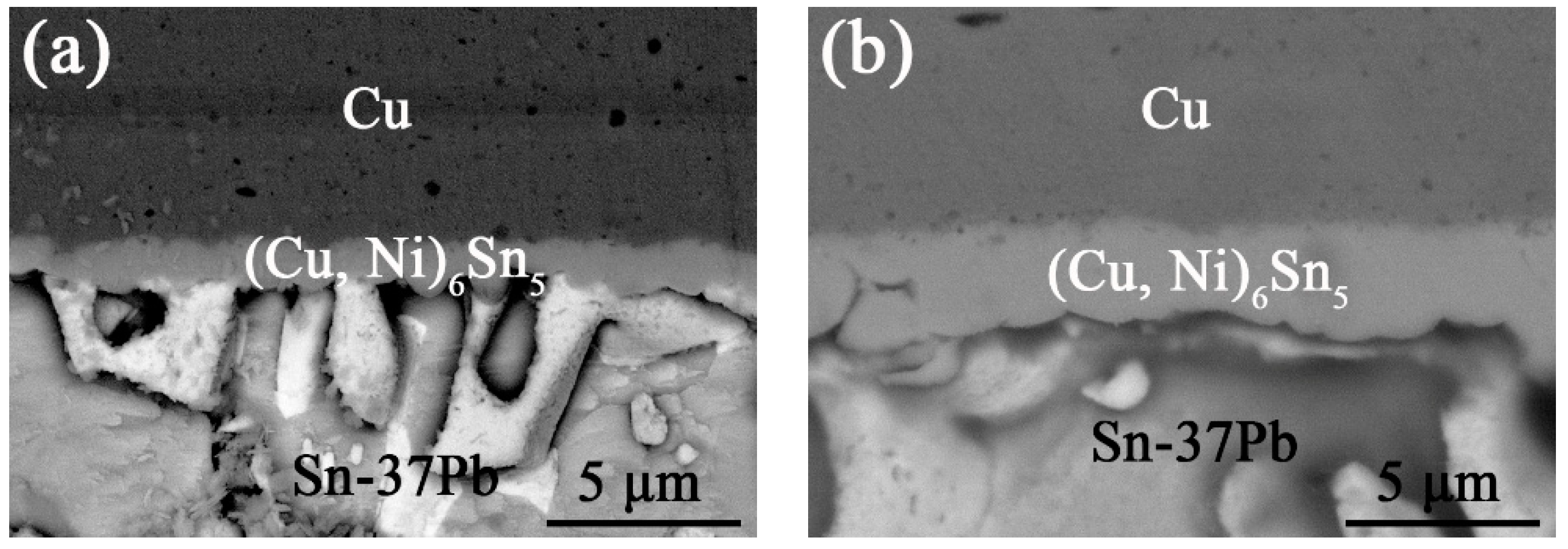
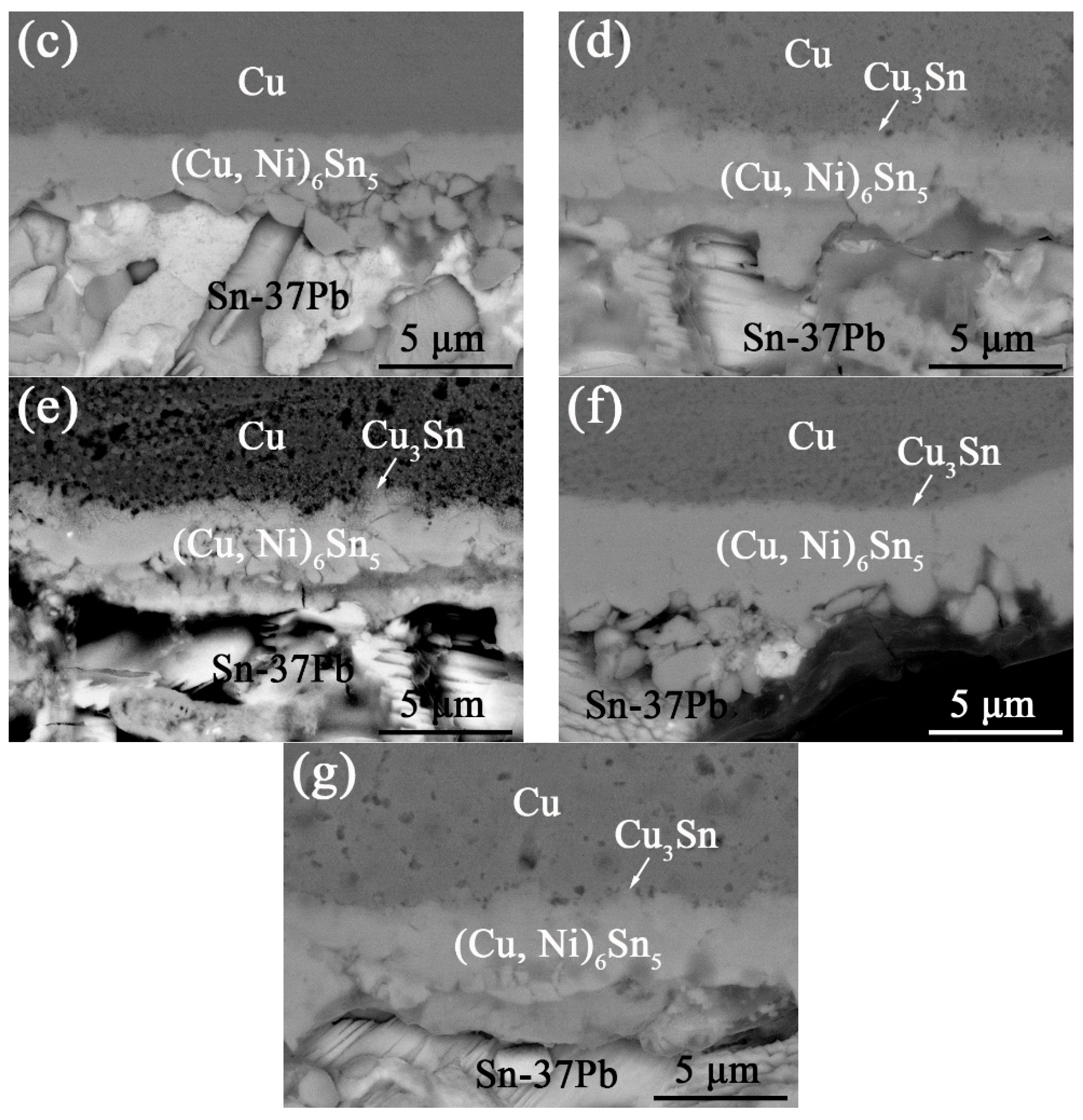
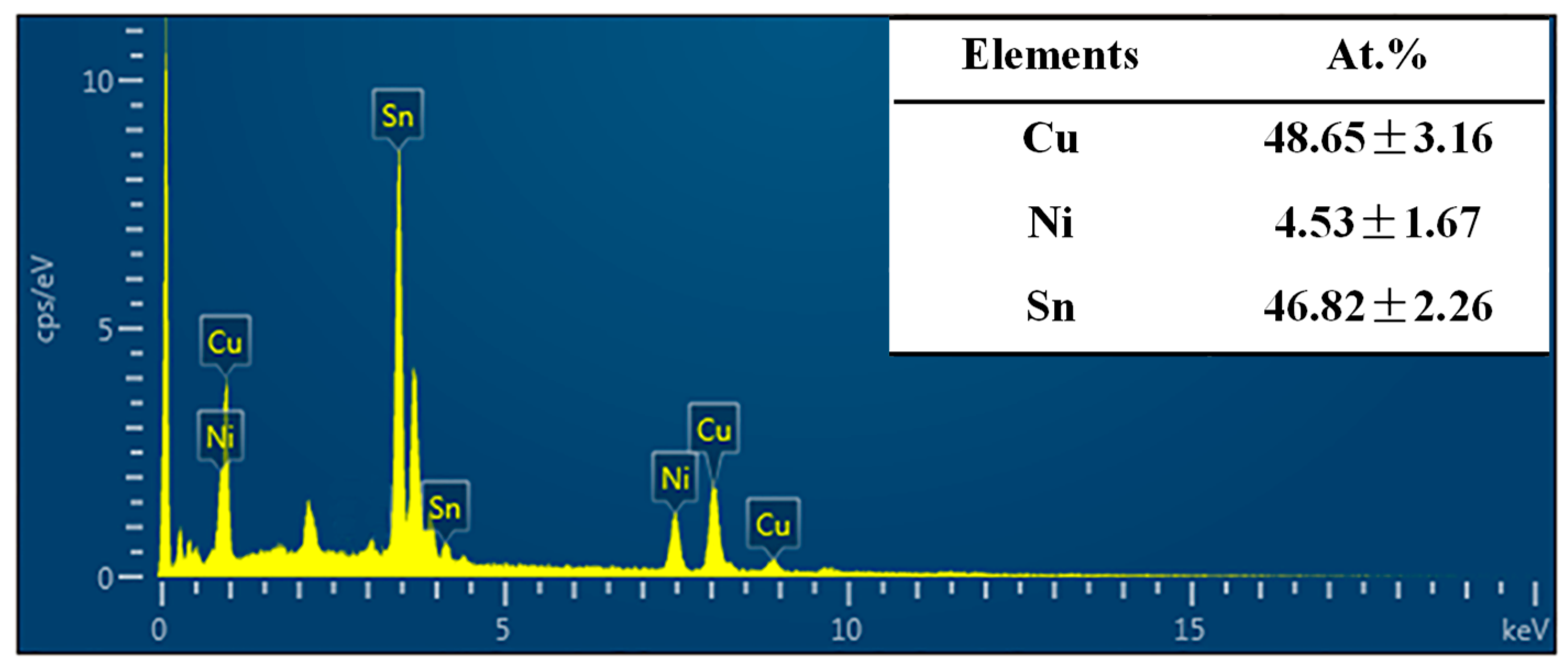
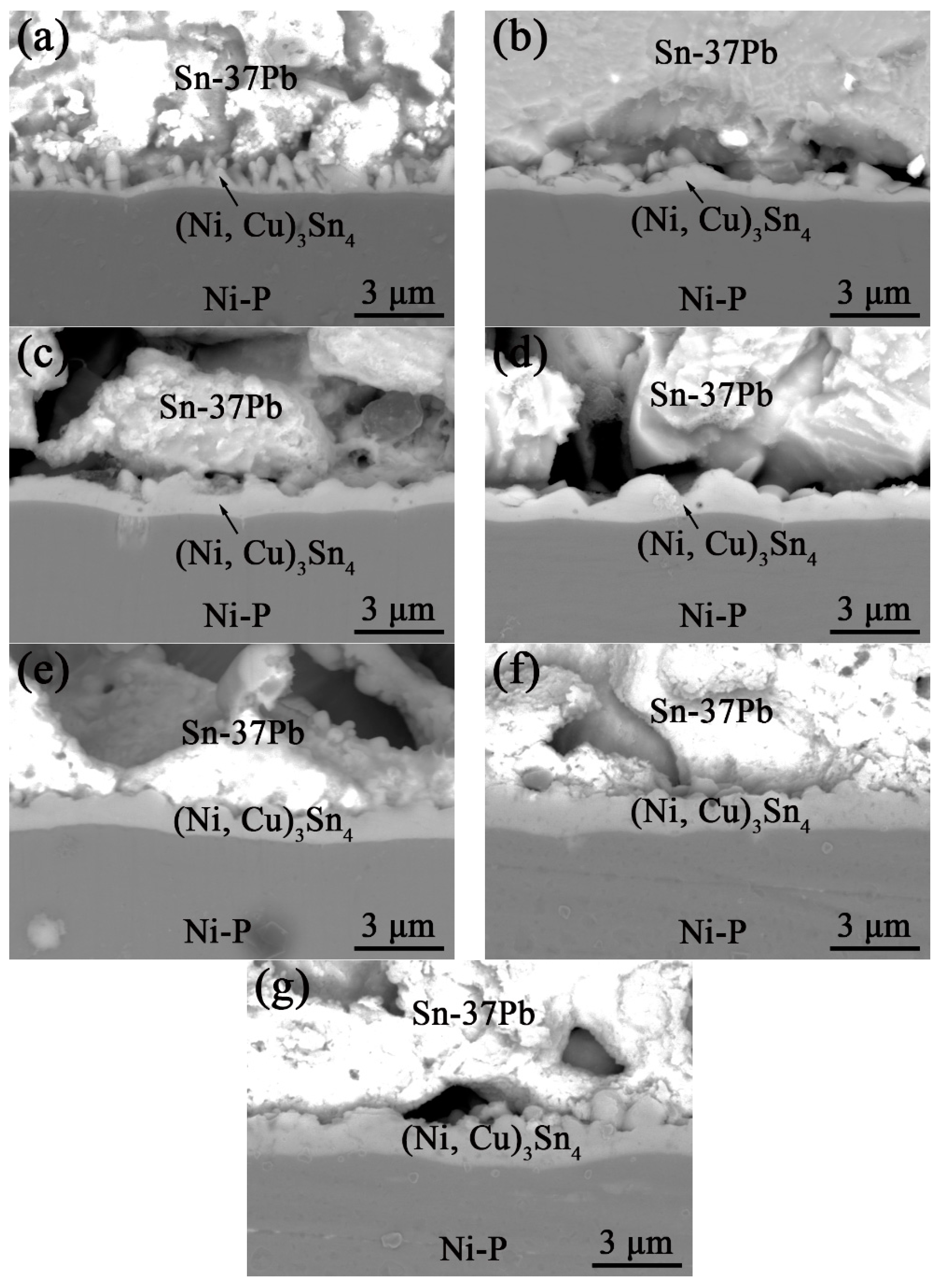
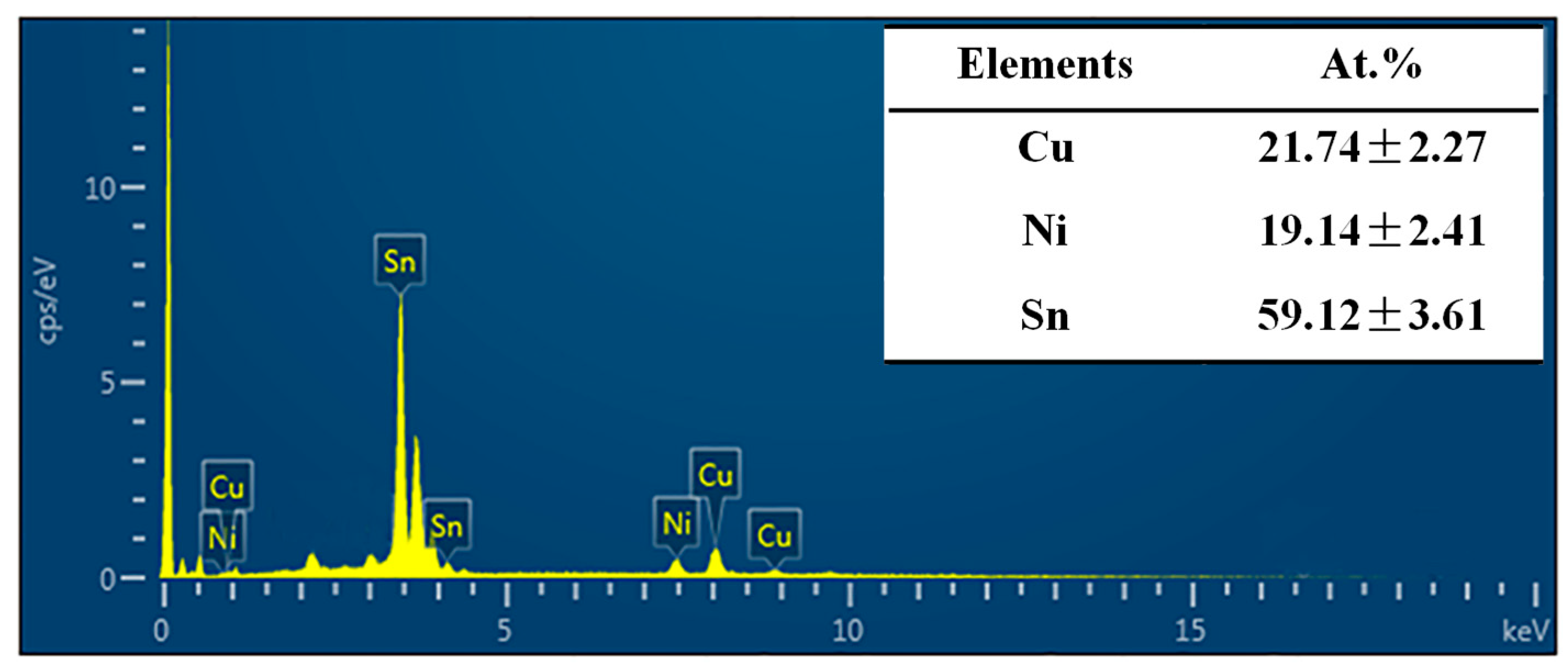
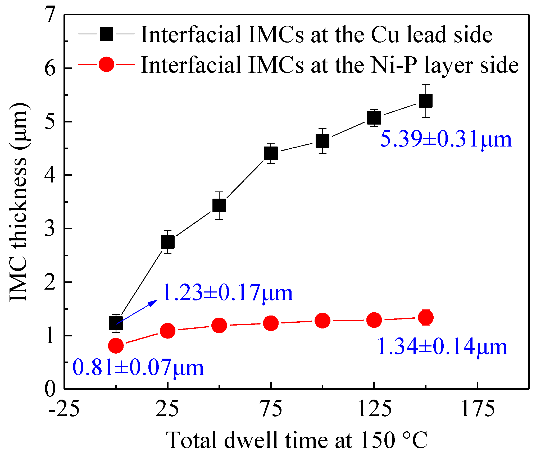
3.1. Microstructure Evolution of Interfacial IMCs

Figure 2 shows the cross-sectional SEM images of the interfacial microstructure between Cu lead and Sn-37Pb solder after reflowing and extreme temperature thermal shock. It could be found that a continuous IMC layer with scallop-type morphology was formed at the interface between Cu lead and Sn-37Pb solder after reflowing, as can be seen in Figure 2a. The chemical compositions of the IMC layer between Cu lead and Sn-37Pb solder was identified by EDS analysis, and the corresponding results is presented in Figure 3. It clearly illustrates that the IMC layer was (Cu, Ni)6Sn5 layer. During reflowing, Cu atoms reacted with Sn atoms to form Cu6Sn5 IMCs, Ni atoms diffused from the opposite Ni-P layer to the Cu lead/solder interface and substituted for Cu atoms in Cu6Sn5 IMCs due to the similarity in crystal structure, which finally led to the transformation of binary Cu6Sn5 compounds to ternary (Cu, Ni)6Sn5 compounds when the Ni content in (Cu, Ni)6Sn5 exceeded 2 at.% [12]. The thickness of interfacial (Cu, Ni)6Sn5 IMCs was 1.23 ± 0.17 μm. During extreme temperature thermal shock, the interfacial IMC thickness obviously increased, and the morphology of interfacial IMCs transformed from scallop-type to plane-type. During extreme temperature thermal shock, Cu atoms of the Cu lead diffused through the interfacial IMCs and reacted with Sn atoms from the Sn-37Pb solder, which resulted in the growth of interfacial IMCs. The shorter diffusion path for Cu atoms contribution to faster growth of IMCs at scallop valleys between the scallop peaks, which resulted in the transformation of IMC morphology from scallop-type to plane-type [13,14]. As seen in Figure 2d, a very thin layer of Cu3Sn IMCs was formed between the Cu lead and (Cu, Ni)6Sn5 IMC layer after 150 cycles. The formation of Cu3Sn between the Cu lead and (Cu, Ni)6Sn5 IMC layer can be attributed to the limited diffusion of Ni from the opposite Ni-P layer. The thickness of the Cu3Sn IMC layer was 107 ± 13 nm. The thickness of the Cu3Sn IMC layer changed little with the increase of thermal shock cycles.
Figure 4 displays the cross-sectional SEM images of the interfacial microstructure between Sn-37Pb solder and Ni-P layer after reflowing and extreme temperature thermal shock. During reflowing, the Au layer was completely dissolved into the molten Sn-37Pb solder due to the high dissolution rate of Au in molten Sn-based solder [15]. Thus, the Ni-P layer was entirely exposed to and reacted with the molten Sn-37Pb solder. A needle-type IMC layer could be observed at the interface between Sn-37Pb solder and Ni-P layer. EDS analysis shows that the IMC layer between the Sn-37Pb solder and Ni-P layer was (Ni, Cu)3Sn4 layer, as shown in Figure 5. The thickness of interfacial (Ni, Cu)3Sn4 IMCs was 0.81 ± 0.7 μm. The thickness of (Ni, Cu)3Sn4 IMC layer gradually increased and the IMC morphology changed from needle-type to scallop-type, and finally to plane-type during extreme temperature thermal shock.

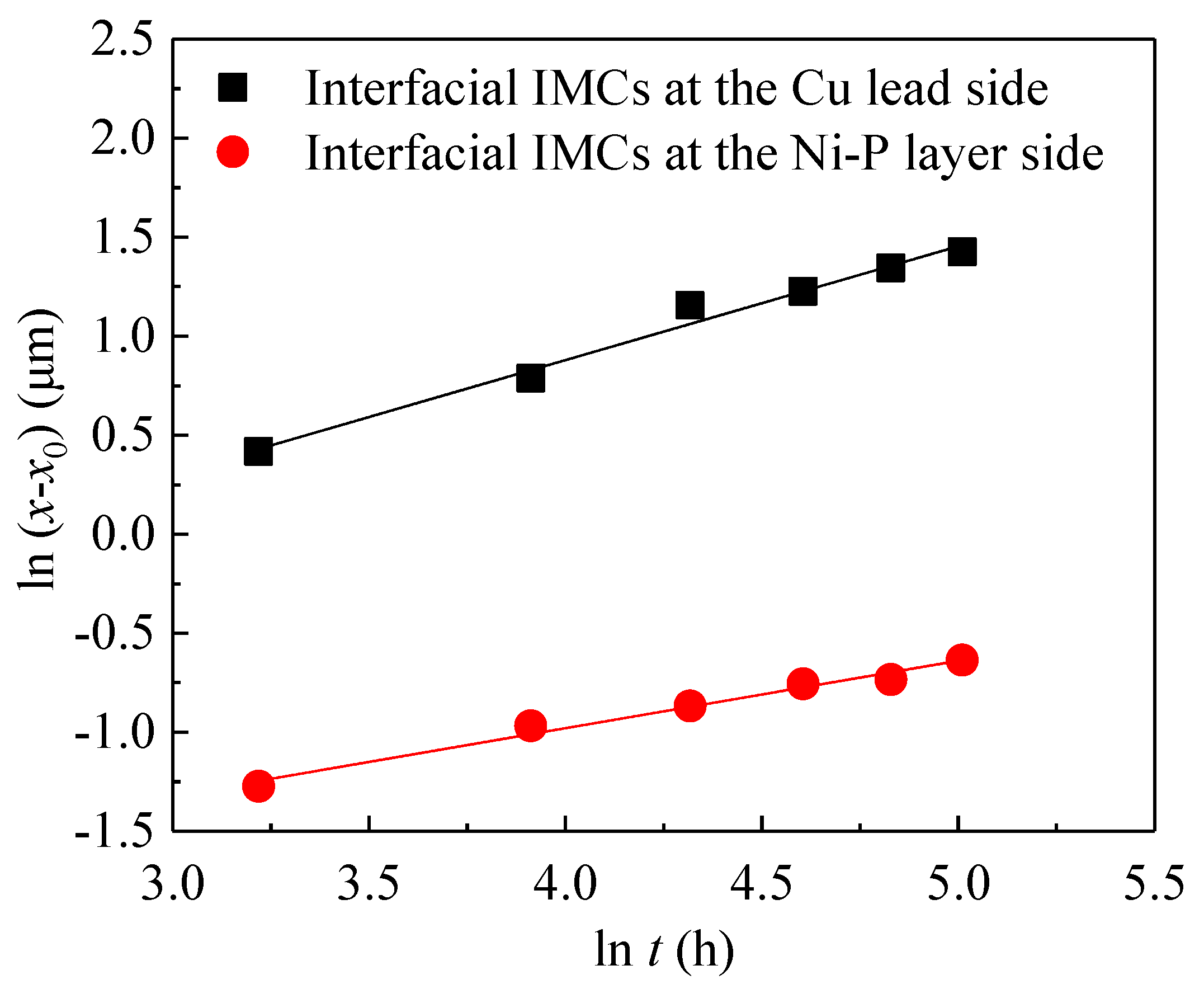
3.2. Growth Mechanism of Interfacial IMCs

Figure 6 shows the thickness of total IMC layer at the lead side and (Ni, Cu)3Sn4 IMC layer at the Ni-P layer side during extreme temperature thermal shock. It is obvious that the IMC layers both at the lead side and at the Ni-P layer side represented a parabolic growth law, implying the growth of IMC layers followed the diffusion-controlled mechanism. The interfacial IMC growth both at the lead side and at the Ni-P layer side became slower with the increase of thermal shock cycles. During extreme temperature thermal shock, Cu, Ni and Sn atoms diffused across the interfacial IMC layer to form IMCs. The IMC layer thickness increased during extreme temperature thermal shock, which obstructed the diffusion of Sn, Cu and Ni atoms and thus suppressed the growth of interfacial IMCs [16,17]. The interfacial IMC growth at the Cu lead side was found to be much faster than that at the Ni-P layer side during extreme temperature thermal shock.
To further study the growth mechanism of interfacial IMCs, an empirical power-law relationship was adopted as follows [17,18]:
x = x0 + A teffn,
where x is the IMC thickness at equivalent time teff, i.e., the total time at the extreme high temperature; x0 is the initial IMC thickness; and A is a constant, and n is the time exponent. Equation (1) is converted into the following logarithmic expression:
ln (xx0) = ln A + n ln t,
The value of the time exponent n was obtained from the slop of the plot of ln (xx0) versus ln t. Figure 7 presents the ln plot of the growth of interfacial IMCs both at the lead side and at the Ni-P layer side during extreme temperature thermal shock. Table 1 lists the values of the time exponent n and the correlation factor R2 for the interfacial IMCs. The n value is considered to be a pointer to the growth mechanism of interfacial IMCs [18,19]. If the n value is closer to 0.33, the IMC growth is dominated by grain-boundary diffusion. If the n value is on the order of 0.5, the IMC growth is dominated by bulk diffusion [18,19]. The values of the time exponent n implied that the growth of the interfacial IMCs at the lead side was dominated by bulk diffusion, and the growth of the interfacial IMCs at the Ni-P layer side was dominated by grain-boundary diffusion under extreme temperature thermal shock. The diffusion mechanism for interfacial IMC growth at the lead side was quite different from that of interfacial IMC growth at the Ni-P layer side. It is presumably due to the differences in initial morphologies, phase constitutions and thicknesses of the interfacial IMCs, which affected the diffusion of atoms across the interfacial IMCs, and thus resulted in various IMC growth mechanisms [20].
In this study, the n value for the interfacial IMC growth at the lead side was higher than 0.5. This can be attributed to the thermal stress generated from the coefficient of thermal expansion (CTE) mismatch between the Cu lead (17 ppm/°C) [17] and the Sn-37Pb solder (24.5 ppm/°C) [21], and the large temperature variation (∆T = 346 °C). The thermal stress near the solder/Cu lead interface contributed to atom diffusion, and thus accelerated the IMC growth process [22].

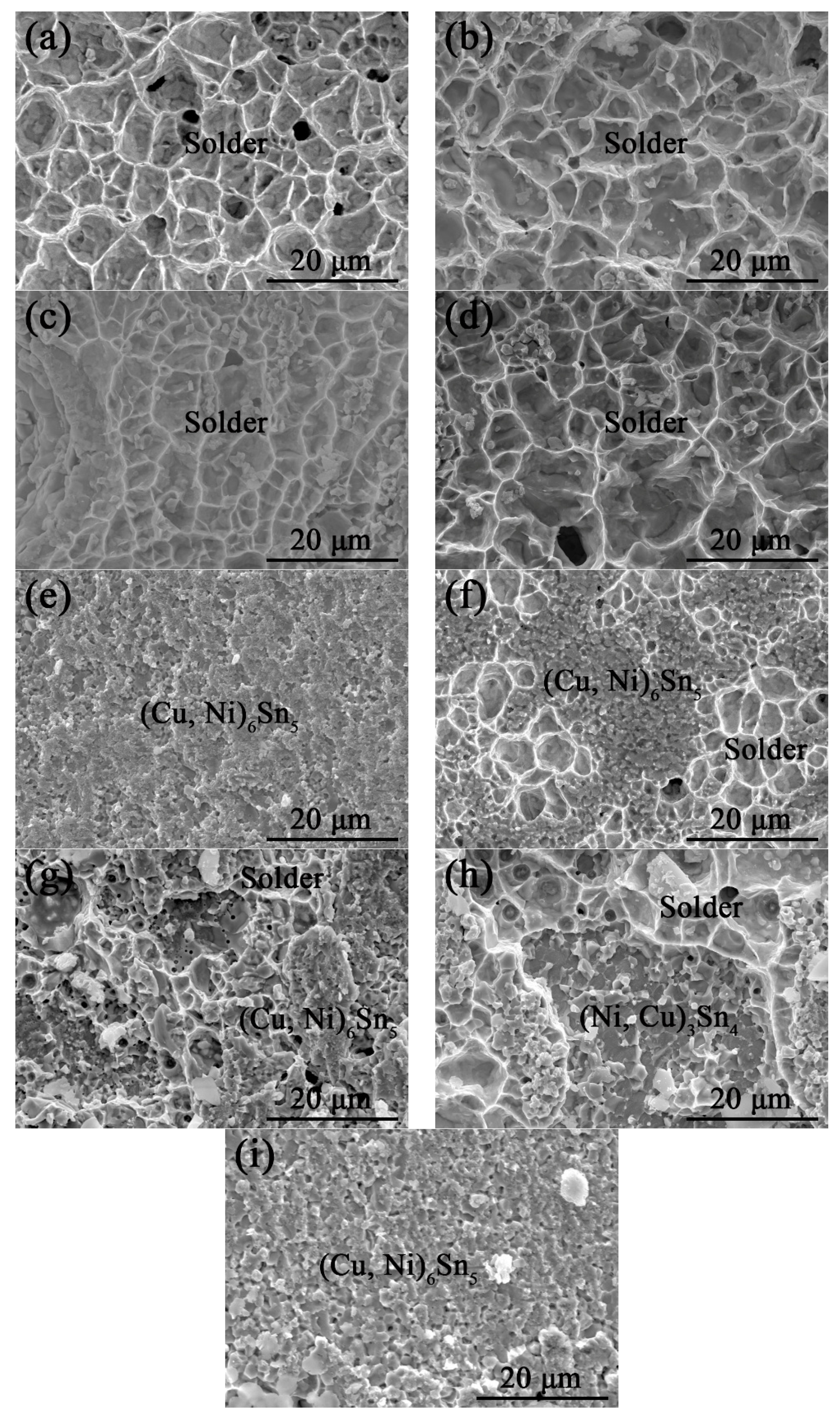
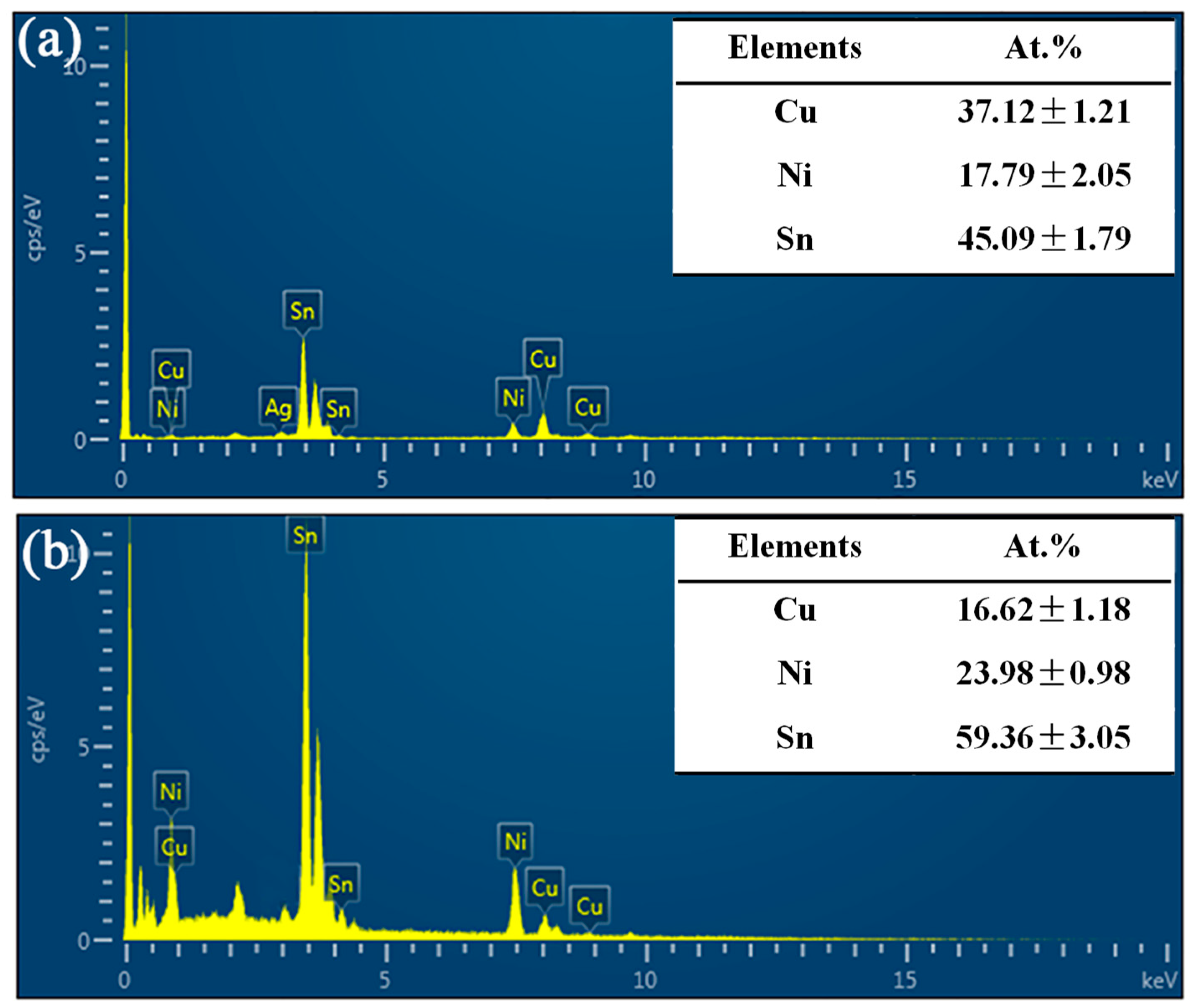
3.3. Mechanical Properties and Fractography

To evaluate the effect of interfacial microstructure evolution on the mechanical property of Sn-37Pb solder joints of QFP assemblies, pull test was carried out. Figure 8 shows the variation of the pull strength with extreme temperature thermal shock. For each condition, at least eight leads of QFPs were pulled to obtain the average value of the pull strength, which resulted in the error in the pull strength. The pull strength of the as-reflowed solder joint was 65.13 MPa. The pull strength declined almost linearly with thermal shock cycles. The pull strength was reduced about 31.54% after 300 cycles. Qian et al. [23] proposed that the failure of solder joints could be defined as more than 50% decline in the solder joint strength. The reduction ratio of the pull strength was lower than 50% after 300 cycles. This indicates that the fatigue life of the solder joint was higher than 300 cycles.
To verify the fracture behavior of Sn-37Pb solder joints, the fracture surfaces were examined using SEM and EDS. Figure 9 shows SEM images of the fracture surfaces of Sn-37Pb solder joints. The fracture surface of Sn-37Pb solder joints after reflowing showed ductile dimple feature (Figure 9a), indicating that the fracture occurred within the solder matrix. The fracture morphologies of solder joints after 50 cycles and 100 cycles are similar to that of solder joints after reflowing, as can be seen in Figure 9b,c. When the interfacial IMCs both at the lead side and the Ni-P layer side were thin, the pull strength of the interfacial IMCs was higher than that of the solder matrix. As a result, fracture tended to occur within the solder matrix, and the pull strength of the solder joints was determined by the solder matrix. CTE mismatch of different constituents in the assembly resulted in cyclic stress and strain in the assemblies, especially in the solder joints during extreme temperature thermal shock [24]. The accumulation of stress and strain induced thermal fatigue and degraded the mechanical properties of the solder matrix, and thus the pull strength of the solder joints declined with extreme temperature thermal shock, as shown in Figure 8.
After 150 cycles, the fracture surface consisted of two different fracture morphologies: dimple and cleavage pattern, and revealing a mixed ductile–brittle fracture (Figure 9d,e). EDS analysis results indicated that the phases with cleavage pattern on the fracture surface were (Cu, Ni)6Sn5 IMCs, as shown in Figure 10a. It is indicated that the crack occurred partially within the solder matrix and partially through the (Cu, Ni)6Sn5 IMC layer. Blair et al. [25] have pointed out that the formation of Ni3Sn4 by solid-state reaction between Ni and Sn caused a 10.7% volume shrinkage, and the formation of Cu6Sn5 by solid-state reaction between Cu and Sn resulted in a 5% volume shrinkage. The growth of interfacial IMCs both at the lead side and at the Ni-P layer side during extreme temperature thermal shock led to volume shrinkage and thus caused stress concentration near the interface. Thick IMC layer was prone to crack initiation due to its brittle nature. The interfacial IMCs grew thicker during extreme temperature thermal shock, and the thickness of (Cu, Ni)6Sn5 IMC layer at the lead side was much higher than that of (Ni, Cu)3Sn4 IMC layer at the Ni-P layer side. Due to the stress concentration near the interface caused by interfacial IMC growth, and the thickening of (Cu, Ni)6Sn5 IMC layer, cracks tended to propagate through the (Cu, Ni)6Sn5 IMC layer under external stress. Consequently, the fracture mode of the solder joints changed from within the solder matrix to a mixed fracture mode of the solder matrix and the (Cu, Ni)6Sn5 IMC layer with the increase of thermal shock cycles. The solder joints after 200 cycles and 250 cycles presented similar fracture morphologies with that after 150 cycles. The area fraction of brittle fracture feature on the fracture surface ascended and the area fraction of ductile fracture feature on the fracture surface descended with the increase of thermal shock cycles. The fracture mechanism of solder joints after 250 cycles was predominated by brittle fracture with minor ductile fracture (Figure 9g). The fatigue of the solder matrix, thickening of the interfacial IMCs, and stress concentration near the interface were responsible for the decline in pull strength of the solder joints with extreme temperature thermal shock. In addition to the solder matrix and (Cu, Ni)6Sn5 IMCs, (Ni, Cu)3Sn4 IMCs were detected on the fracture surface of solder joints after 300 cycles; the EDS analysis results of (Ni, Cu)3Sn4 IMCs on the fracture surface is shown in Figure 10b. It reveals that the solder joints after 300 cycles fractured through the solder matrix, (Cu, Ni)6Sn5 IMC layer, and the (Ni, Cu)3Sn4 IMC layer.

4. Conclusions

In this study, extreme temperature thermal shock test from −196 °C to 150 °C was conducted on QFP assemblies with Sn-37Pb solder joints to investigate the evolution and growth behavior of interfacial IMCs and their effect on the pull strength and fracture behavior of Sn-37Pb solder joints under extreme temperature environment. The following conclusions were obtained:
(1)
A continuous (Cu, Ni)6Sn5 IMC layer was formed at the interface between the Cu lead and the Sn-37Pb solder after reflowing, and the IMCs formed between the solder and Ni-P layer was (Ni, Cu)3Sn4 IMCs. A thin layer of Cu3Sn IMCs was formed between the Cu lead and (Cu, Ni)6Sn5 IMC layer after 150 cycles.
(2)
The morphology of interfacial (Cu, Ni)6Sn5 IMCs changed from scallop-type to plane-type, and the morphology of interfacial (Ni, Cu)3Sn4 IMCs evolved from needle-type to scallop-type, and finally to plane-type during extreme temperature thermal shock.
(3)
The thickness of the interfacial IMCs both at the Cu lead side and at the Ni-P layer side gradually increased with extreme temperature thermal shock. The growth of interfacial IMCs at the Cu lead side was found to be much faster than that at the Ni-P layer side. The growth of the interfacial IMCs at the lead side was dominated by bulk diffusion, and the growth of the interfacial (Ni, Cu)3Sn4 IMCs at the Ni-P layer side was dominated by grain-boundary diffusion.
(4)
With increasing thermal shock cycles, the pull strength of the joints decreased, and the fracture mechanism changed from ductile fracture to mixed ductile–brittle fracture. The pull strength was reduced about 31.54% after 300 cycles.

Author Contributions

R.T. conceived and performed the experiments, analyzed the data, and wrote the paper. C.H. and Y.T. provided the experimental materials and laboratory equipment, and directed the research.

Acknowledgments

This work was supported by the National Natural Science Foundation of China (Grant No. 51522503), the National Natural Science Foundation of China (Grant No. 51775141), and the Program for New Century Excellent Talents in University (NCET-13-0175).

Conflicts of Interest

The authors declare no conflict of interest.

References

  1. Rahim, M.K.; Suhling, J.C.; Jaeger, R.C.; Lall, P.; Knight, R. Reliability of flip chip assemblies subjected to extreme low temperatures. In Proceedings of the 10th Intersociety Conference on Thermal and Thermomechanical Phenomena in Electronic Systems, San Diego, CA, USA, 30 May–2 June 2006; pp. 1379–1389. [Google Scholar]
  2. Yoon, J.M.; Chun, H.S.; Koo, J.M.; Lee, H.J.; Jung, S.B. Microstructural evolution of Sn-rich Au-Sn/Ni flip-chip solder joints under high temperature storage testing conditions. Scr. Mater. 2007, 56, 661–664. [Google Scholar] [CrossRef]
  3. Sharif, A.; Islam, M.N.; Chan, Y.C. Interfacial reactions of BGA Sn-3.5%Ag-0.5%Cu and Sn-3.5%Ag solders during high-temperature aging with Ni/Au metallization. Mater. Sci. Eng. B 2004, 113, 184–189. [Google Scholar] [CrossRef]
  4. Lee, H.T.; Chen, M.H.; Jao, H.M.; Liao, T.L. Influence of interfacial intermetallic compound on fracture behavior of solder joints. Mater. Sci. Eng. A 2003, 358, 134–141. [Google Scholar] [CrossRef]
  5. Xue, P.; Xue, S.; Zhang, L.; Shen, Y.F.; Gao, L.L.; Yu, S.L.; Zhu, H.; Han, Z.L.; Chen, Y. Tensile strength of fine pitch QFP lead-free soldered joints with diode laser soldering. Solder. Surf. Mt. Technol. 2011, 23, 177–183. [Google Scholar] [CrossRef]
  6. Ma, Y.; Wu, T.; Liu, W.; Huang, Y.F.; Tang, S.W.; Wang, Y.K. Interfacial microstructure evolution and shear behavior of Au–12Ge/Ni solder joints during isothermal aging. J. Mater. Sci. Mater. Electron. 2017, 28, 3685–3694. [Google Scholar] [CrossRef]
  7. Deng, X.; Sidhu, R.S.; Johnson, P.; Chawla, N. Influence of reflow and thermal aging on the shear strength and fracture behavior of Sn-3.5Ag solder/Cu joints. Metall. Mater. Trans. A 2005, 36, 55–64. [Google Scholar] [CrossRef]
  8. Kim, D.G.; Kim, J.W.; Jung, S.B. Effect of aging conditions on interfacial reaction and mechanical joint strength between Sn-3.0Ag-0.5Cu solder and Ni-P UBM. Mater. Sci. Eng. B 2005, 121, 204–210. [Google Scholar] [CrossRef]
  9. Tian, R.Y.; Hang, C.J.; Tian, Y.H.; Zhao, L.Y. Growth behavior of intermetallic compounds and early formation of cracks in Sn-3Ag-0.5Cu solder joints under extreme temperature thermal shock. Mater. Sci. Eng. A 2018, 709, 125–133. [Google Scholar] [CrossRef]
  10. Ghaffarian, R. CCGA packages for space applications. Microelectron. Reliab. 2006, 46, 2006–2024. [Google Scholar] [CrossRef]
  11. Li, X.Y.; Li, F.H.; Guo, F.; Shi, Y.W. Effect of isothermal aging and thermal cycling on interfacial IMC growth and fracture behavior of SnAgCu/Cu joints. J. Electron. Mater. 2001, 40, 51–61. [Google Scholar] [CrossRef]
  12. Zeng, K.; Vuorinen, V.; Kivilahti, J.K. Interfacial reactions between lead-free SnAgCu solder and Ni(P) surface finish on printed circuit boards. IEEE Trans. Electron. Packag. Manuf. 2002, 25, 162–167. [Google Scholar] [CrossRef]
  13. Deng, X.; Piotrowski, G.; Williams, J.J.; Chawla, N. Influence of initial morphology and thickness of Cu6Sn5 and Cu3Sn intermetallics on growth and evolution during thermal aging of Sn-Ag solder/Cu joints. J. Electron. Mater. 2003, 32, 1403–1413. [Google Scholar] [CrossRef]
  14. Shen, J.; Zhao, M.; He, P.; Pu, Y. Growth behaviors of intermetallic compounds at Sn-3Ag-0.5Cu/Cu interface during isothermal and non-isothermal aging. J. Alloys Compd. 2013, 574, 451–458. [Google Scholar] [CrossRef]
  15. Davis, J.A.; Bozack, M.J.; Evans, J.L. Effect of (Au, Ni)Sn4 evolution on Sn-37Pb/ENIG solder joint reliability under isothermal and temperature-cycled conditions. IEEE Trans. Compon. Packag. Technol. 2007, 30, 32–41. [Google Scholar] [CrossRef]
  16. Shen, J.; Zhai, D.; Cao, Z.; Zhao, M.; Pu, Y. Fracture behaviors of Sn-Cu intermetallic compound layer in ball grid array induced by thermal shock. J. Electron. Mater. 2013, 43, 567–578. [Google Scholar] [CrossRef]
  17. Xia, Y.H.; Me, X.M. Reliability of lead-free solder joints with different PCB surface finishes under thermal cycling. J. Alloys Compd. 2008, 454, 174–179. [Google Scholar] [CrossRef]
  18. Tu, P.L.; Chan, Y.C.; Hung, K.C.; Lai, J.K.L. Growth kinetics of intermetallic compounds in chip scale package solder joint. Scr. Mater. 2001, 44, 317–323. [Google Scholar] [CrossRef] [Green Version]
  19. Choudhury, S.F.; Ladani, L. Local shear stress-strain response of Sn-3.5Ag/Cu solder joint with high fraction of intermetallic compounds: Experimental analysis. J. Alloys Compd. 2016, 680, 665–676. [Google Scholar] [CrossRef] [Green Version]
  20. Xu, L.H.; Pang, J.H.L.; Prakash, K.H.; Low, T.H. Isothermal and thermal cycling aging on IMC growth rate in lead-free and lead-based solder interface. IEEE Trans. Compon. Packag. Technol. 2005, 28, 408–414. [Google Scholar] [CrossRef]
  21. Perkins, A.; Sitaraman, S.K. Analysis and prediction of vibration-induced solder joint failure for a ceramic column grid array package. J. Electron. Packag. 2008, 130, 011012. [Google Scholar] [CrossRef]
  22. Pang, J.H.L.; Xu, L.H.; Shi, X.Q.; Zhou, W.; Ngoh, S.L. Intermetallic growth studies on Sn-Ag-Cu lead-free solder joints. J. Electron. Mater. 2004, 33, 1219–1226. [Google Scholar] [CrossRef]
  23. Qian, Z.F.; Liu, S. On the life prediction and accelerated testing of solder joints. Int. J. Microcircuits Electron. Packag. 1999, 22, 288–304. [Google Scholar] [CrossRef]
  24. Zhang, B.; Ding, H.; Sheng, X. Reliability study of board-level lead-free interconnections under sequential thermal cycling and drop impact. Microelectron. Reliab. 2009, 49, 530–536. [Google Scholar] [CrossRef]
  25. Blair, H.D.; Pan, T.Y.; Nicholson, J.M. Intermetallic compound growth on Ni, Au/Ni, and Pd/Ni substrates with Sn/Pb, Sn/Ag, and Sn solders. In Proceedings of the 48th Electronic Components & Technology Conference, Seattle, WA, USA, 25–28 May 1998; pp. 259–267. [Google Scholar]
Figure 1. The cross section of Sn-37Pb solder joints after reflowing.
Applsci 08 02056 g001
Figure 2. SEM images of the Cu lead/Sn-37Pb solder interface: (a) after reflowing; (b) after 50 cycles; (c) after 100 cycles; (d) after 150 cycles; (e) after 200 cycles; (f) after 250 cycles; and (g) after 300 cycles.
Applsci 08 02056 g002aApplsci 08 02056 g002b
Figure 3. EDS analysis of the IMC layer between Cu lead and the Sn-37Pb solder.
Applsci 08 02056 g003
Figure 4. SEM images of the Sn-37Pb solder/Ni-P layer interface: (a) after reflowing; (b) after 50 cycles; (c) after 100 cycles; (d) after 150 cycles; (e) after 200 cycles; (f) after 250 cycles; and (g) after 300 cycles.
Applsci 08 02056 g004
Figure 5. EDS analysis of the IMC layer between the Sn-37Pb solder and Ni-P layer.
Applsci 08 02056 g005
Figure 6. The thickness of interfacial Cu-Sn IMCs and Ni-Cu-Sn IMCs during extreme temperature thermal shock.
Applsci 08 02056 g006
Figure 7. Ln plot of the growth of interfacial IMCs during extreme temperature thermal shock.
Applsci 08 02056 g007
Figure 8. The variation of the pull strength of Sn-37Pb solder joints with extreme temperature thermal shock. The percentage in this figure represents the reduction ratio of the pull strength with extreme temperature thermal shock.
Applsci 08 02056 g008
Figure 9. SEM images of the fracture surfaces of Sn-37Pb solder joints: (a) after reflowing; (b) after 50 cycles; (c) after 100 cycles; (d,e) after 150 cycles; (f) after 200 cycles; (g) after 250 cycles; and (h,i) after 300 cycles.
Applsci 08 02056 g009
Figure 10. EDS analysis results of: (a) (Cu, Ni)6Sn5 IMCs; and (b) (Ni, Cu)3Sn4 IMCs on the fracture surface.
Applsci 08 02056 g010
Table 1. Time exponent of the interfacial IMCs.
Interfacial IMCsTime Exponent nCorrelation Factor R2
Interfacial IMCs at the lead side0.570.98
Interfacial IMCs at the Ni-P layer side0.340.98

