Reduction of Bias and Light Instability of Mixed Oxide Thin-Film Transistors

Abstract
:Featured Application
Abstract

1. Introduction
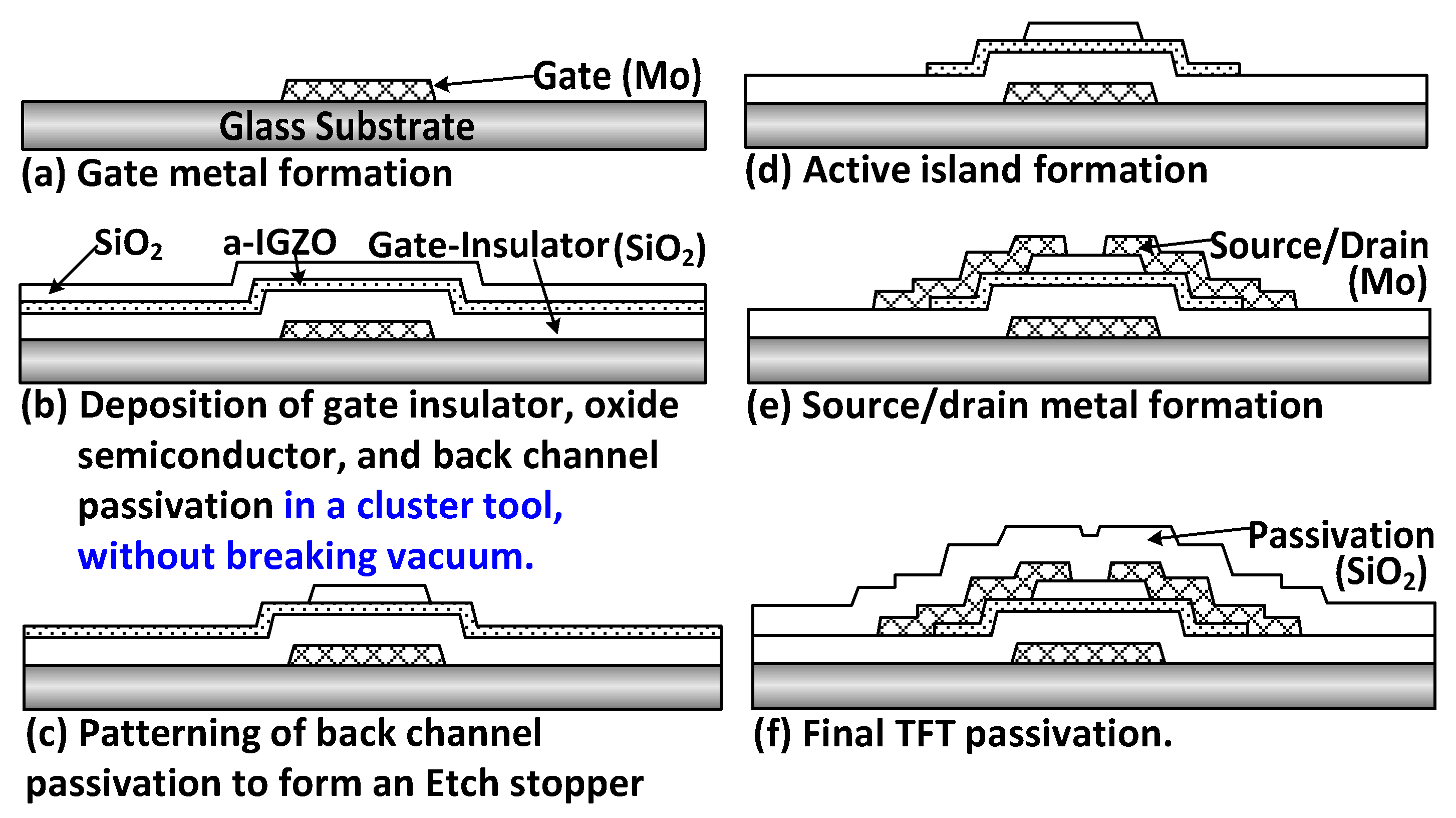
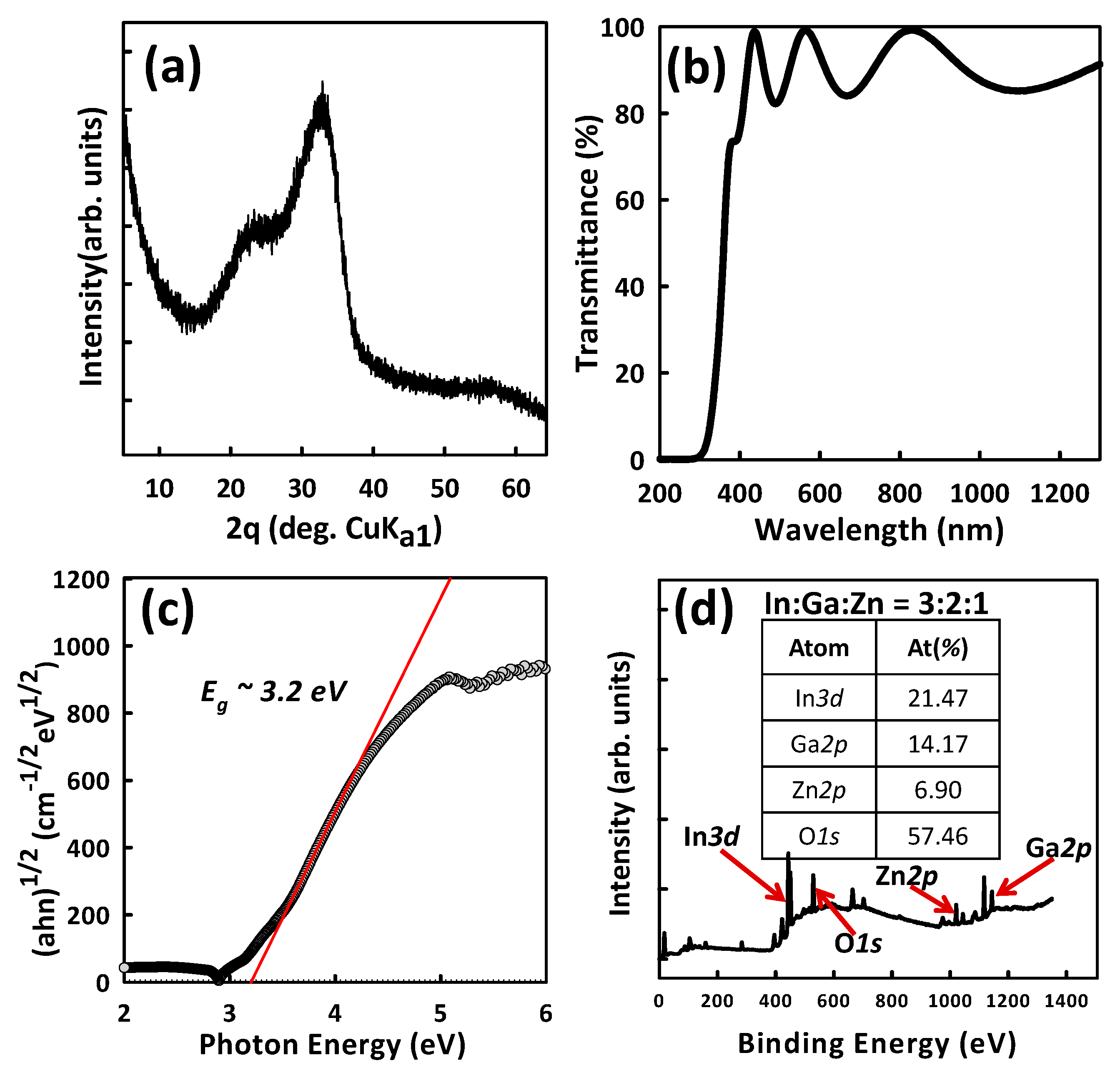
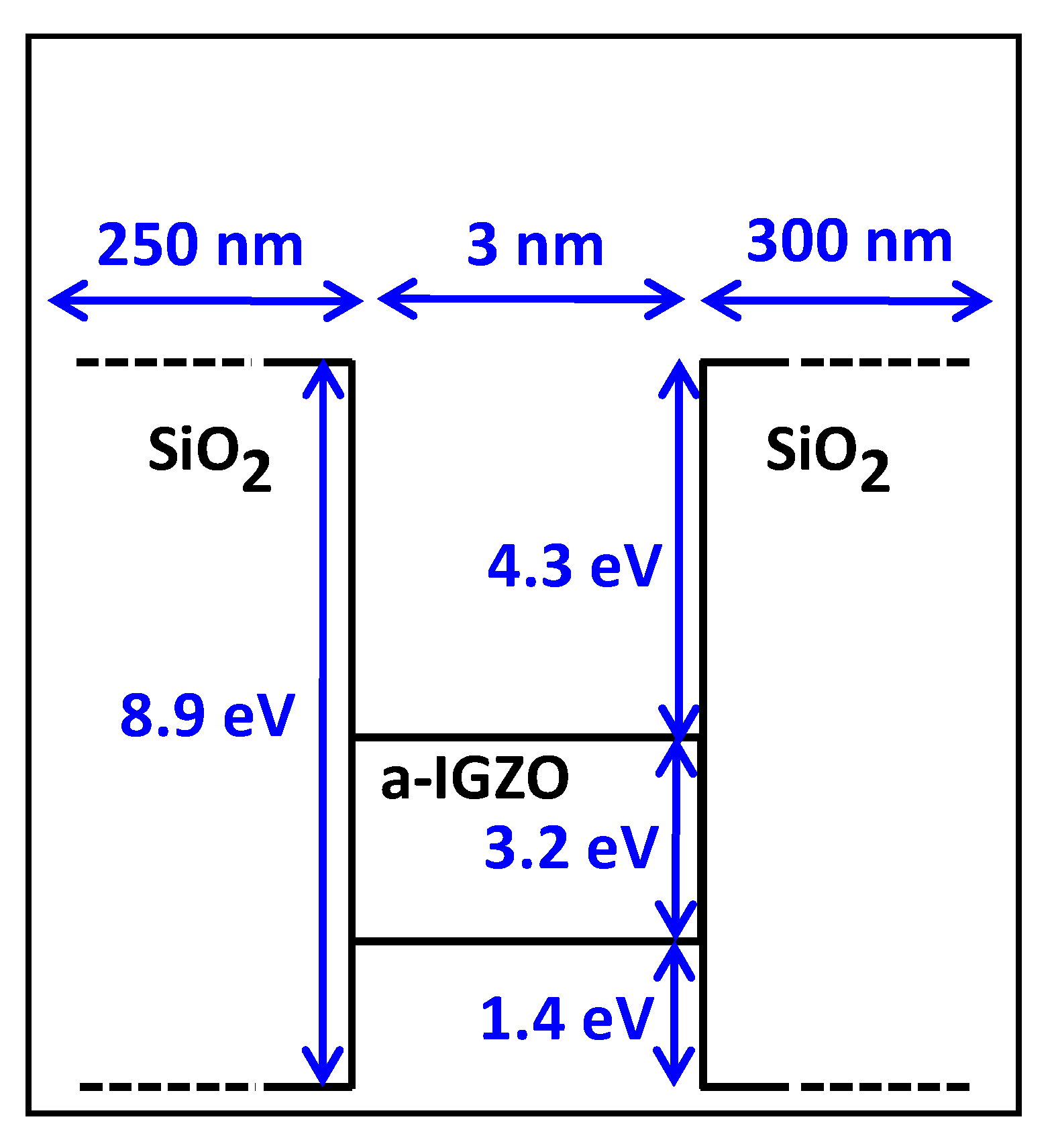
2. Materials and Methods
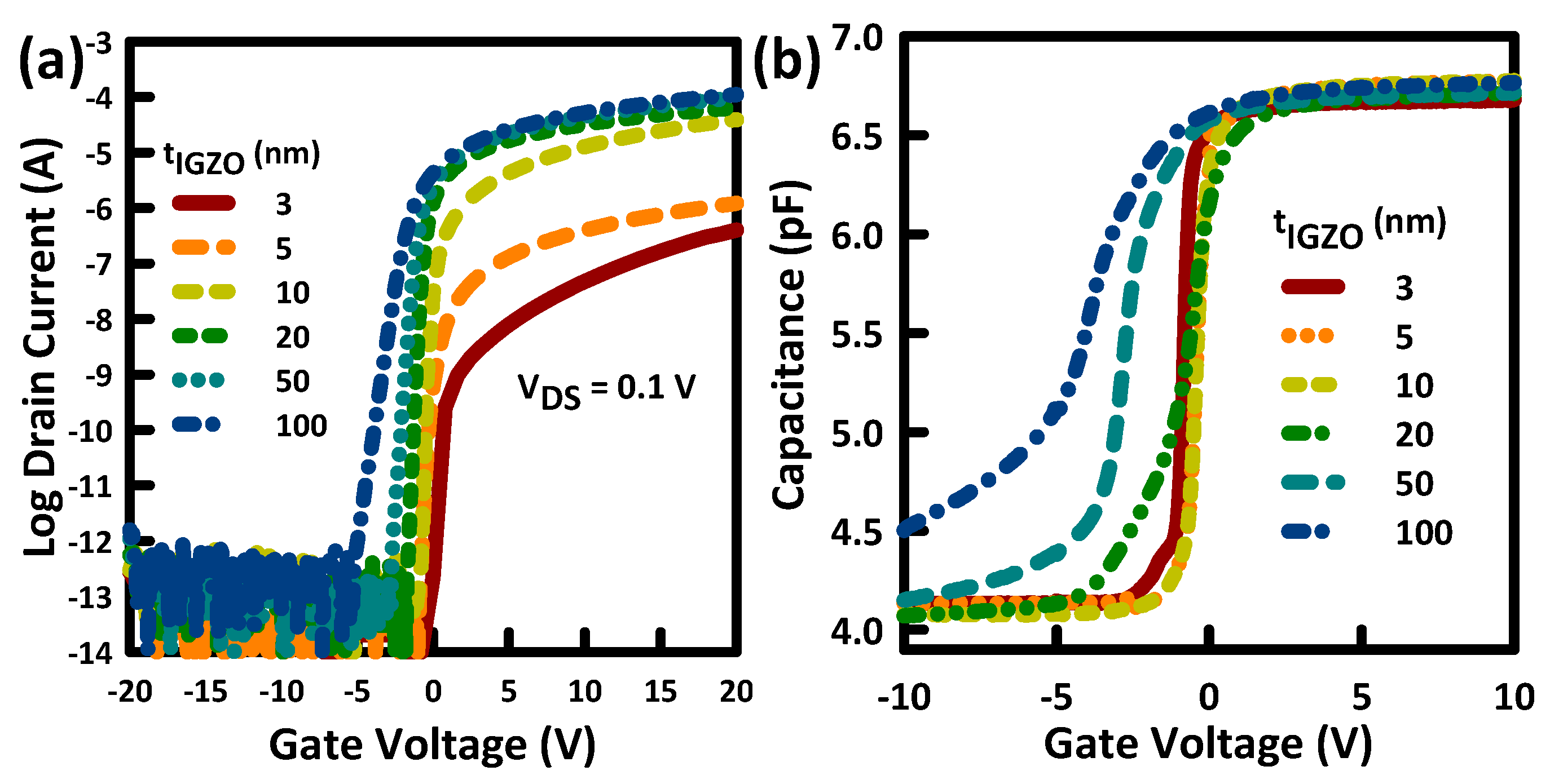
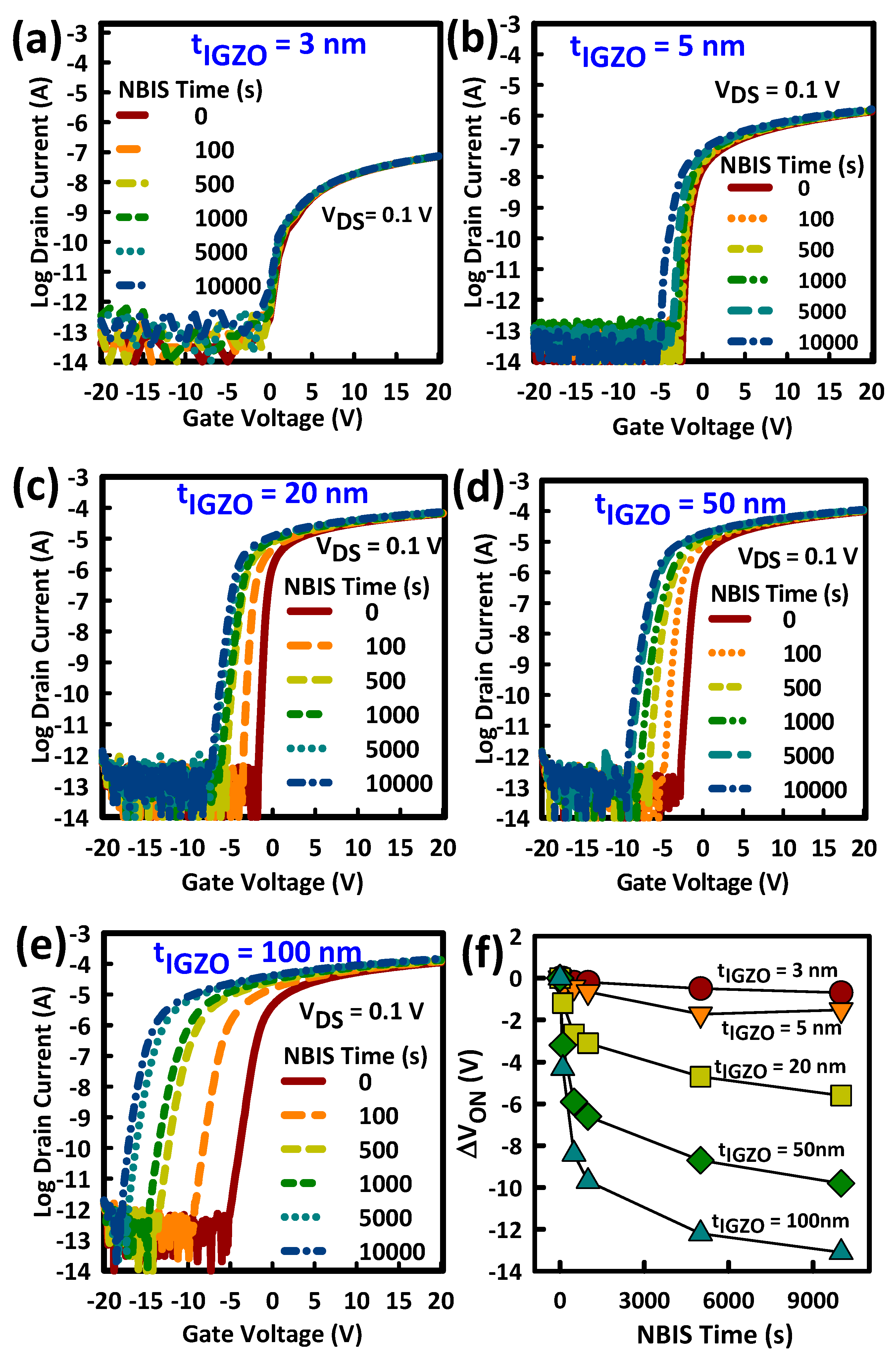
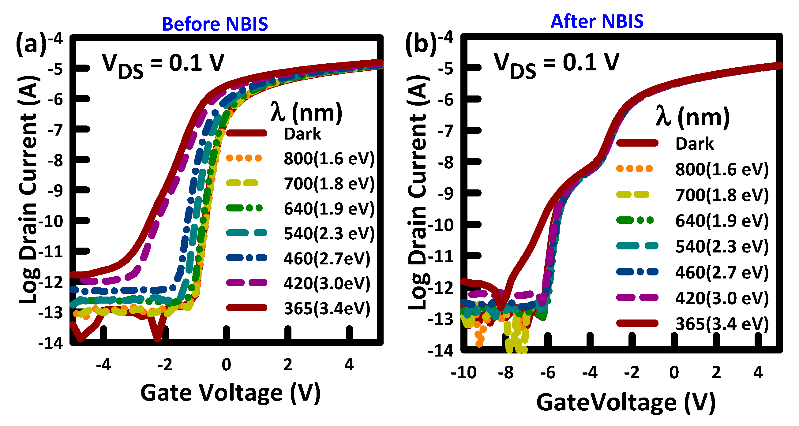
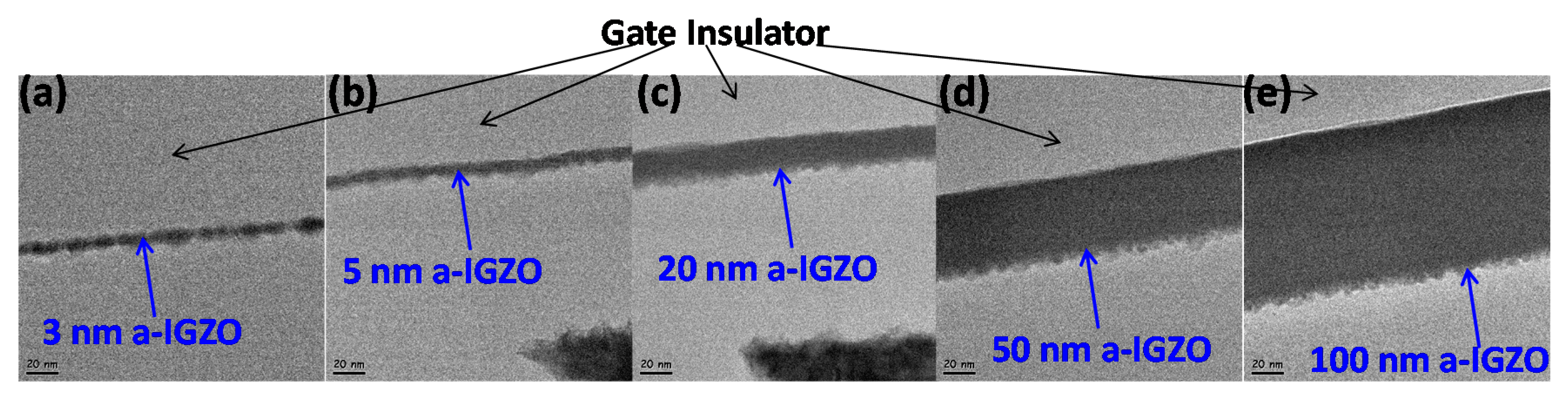
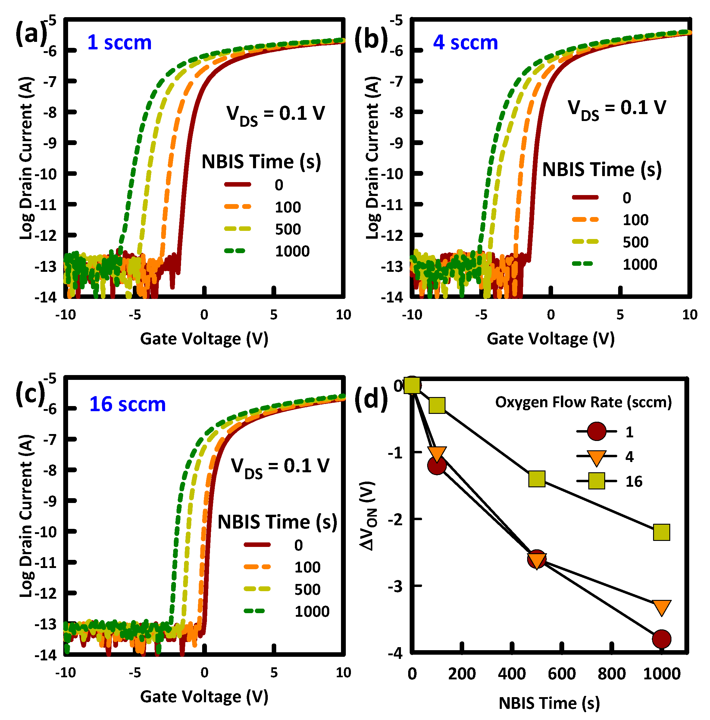
3. Results
4. Discussion
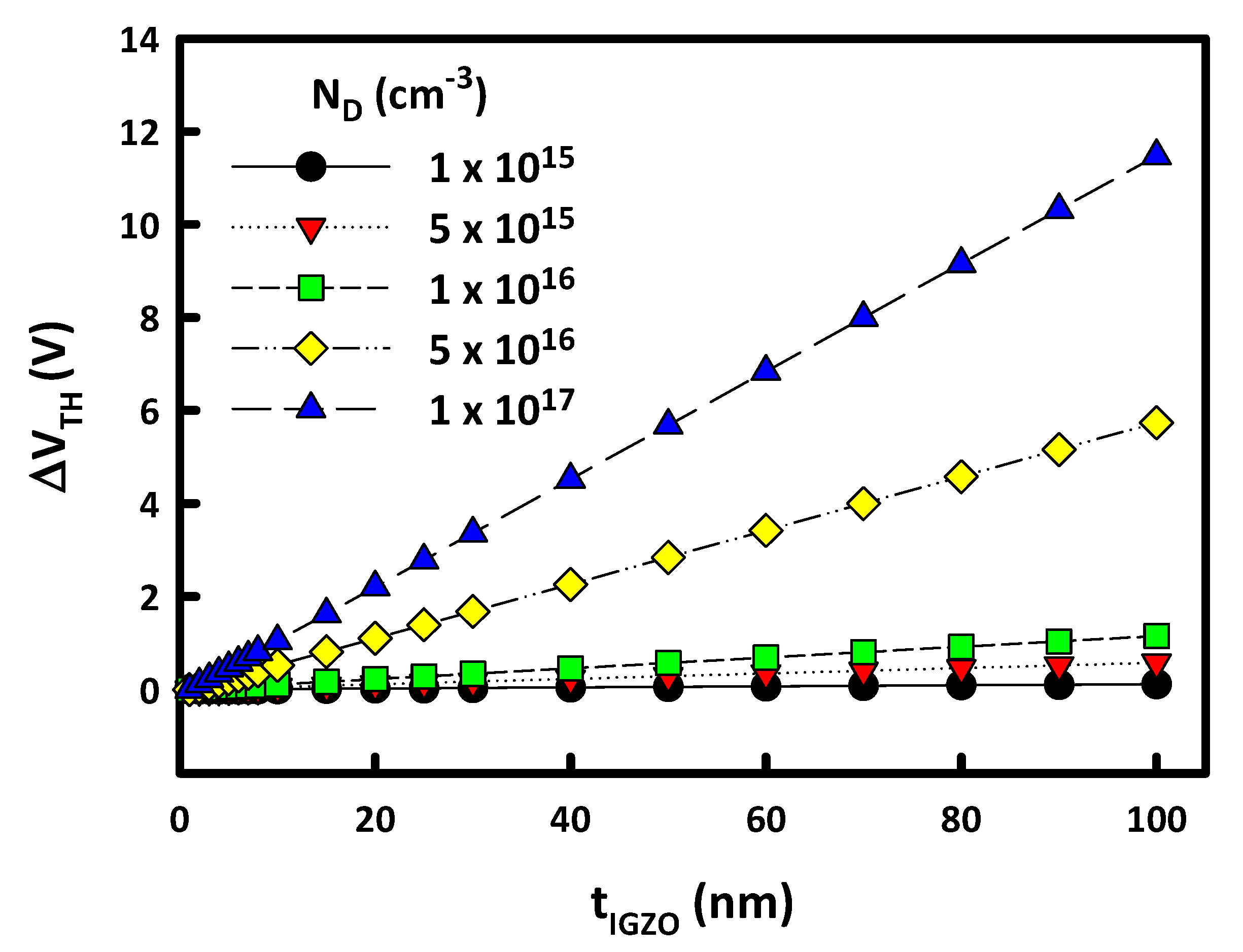
4.1. VTH Dependency on Channel Thickness
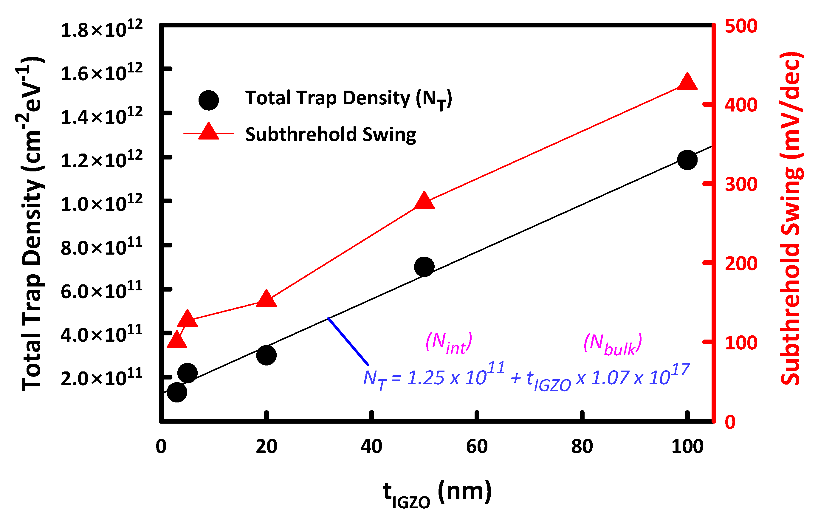
4.2. SS Dependency on Channel Thickness
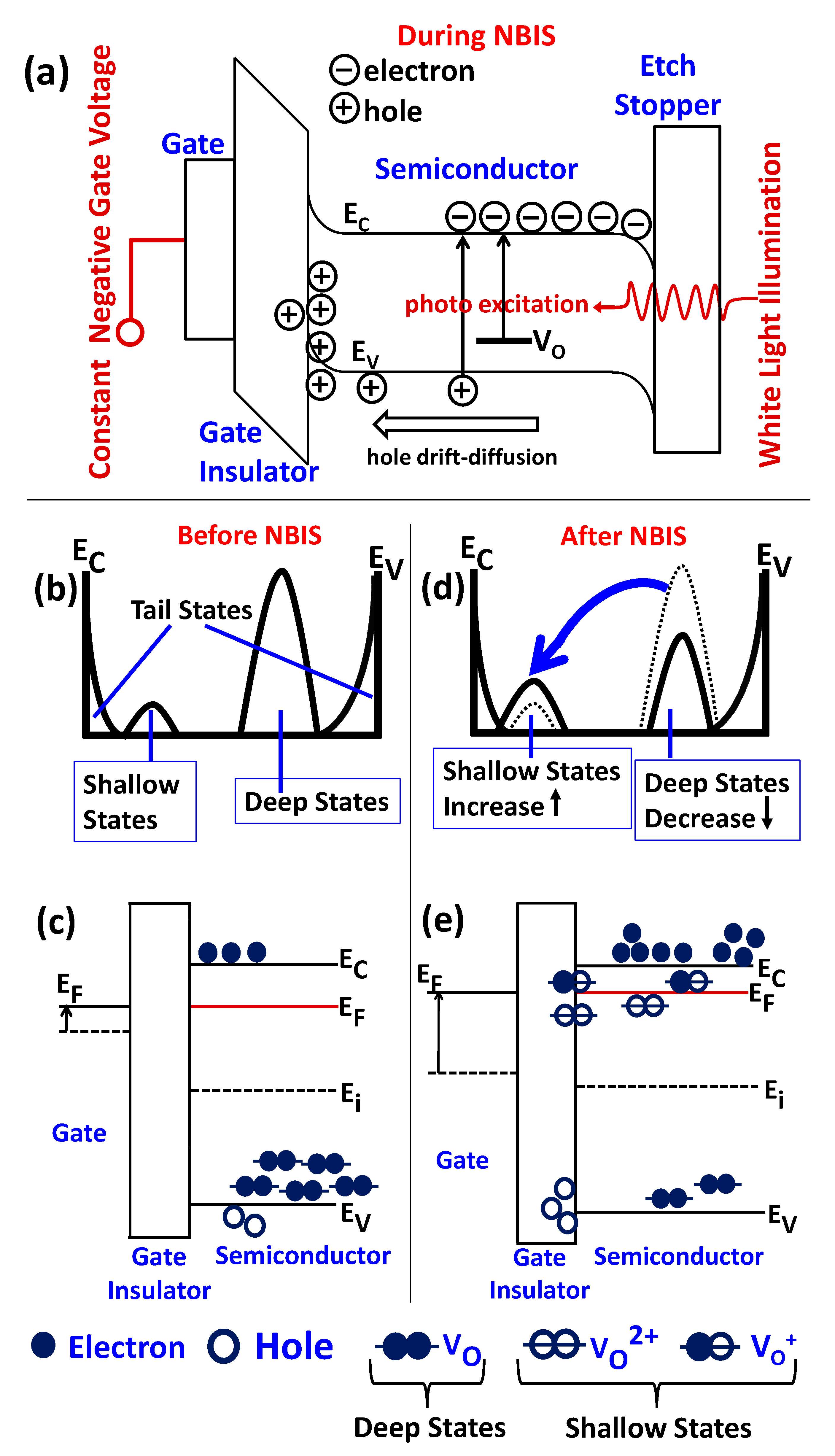
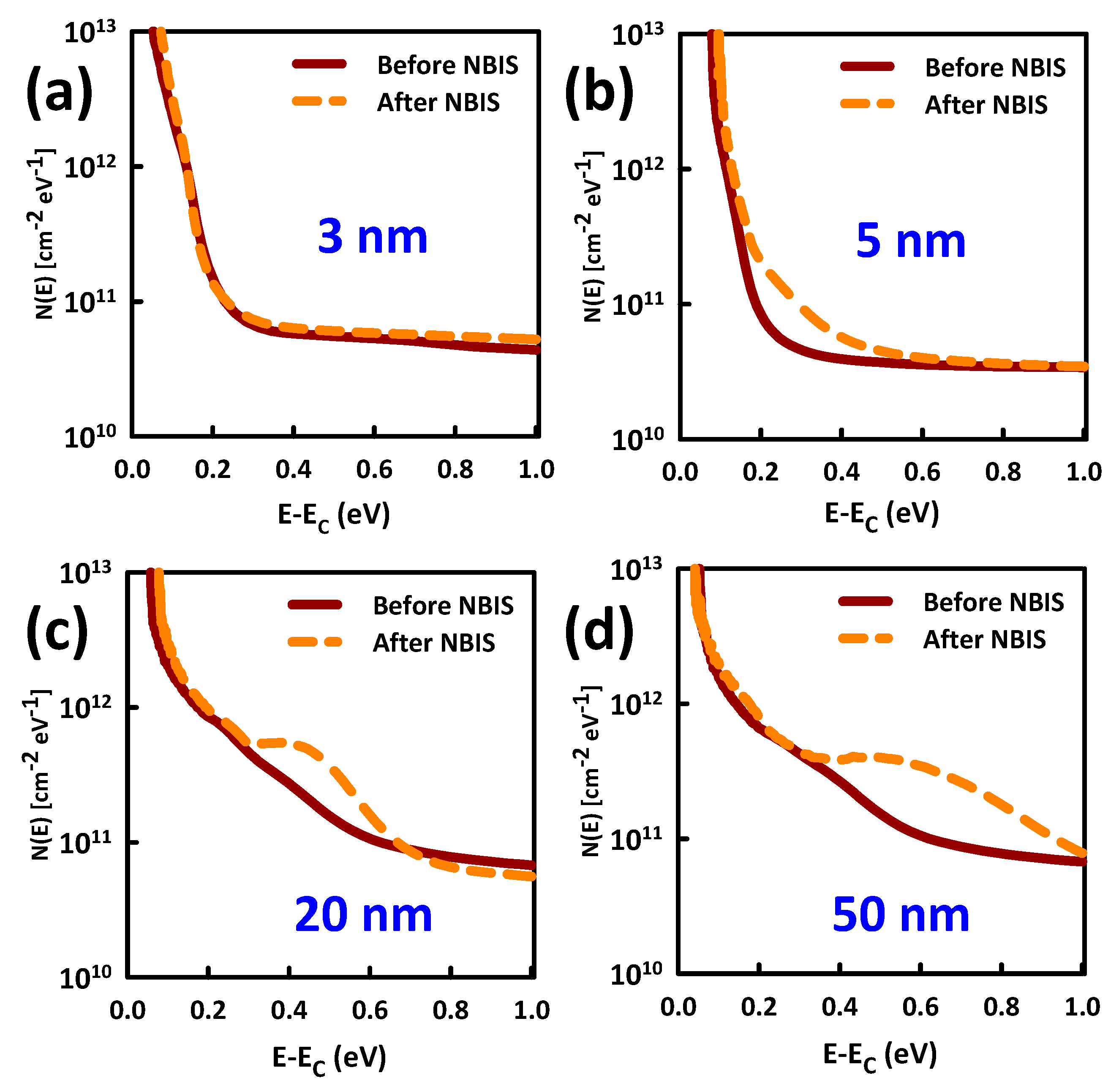
4.3. Effect of Channel Thickness on NBIS Stability
4.4. Verification of the Effect of Oxygen Vacancies on NBIS Stability
4.5. Fabrication Process Optimization
Acknowledgments
Author Contributions
Conflicts of Interest
References
- Kamiya, T.; Hosono, H. Material characteristics and applications of transparent amorphous oxide semiconductors. NPG Asia Mater. 2010, 2, 15–22. [Google Scholar] [CrossRef]
- Jeong, J.K. The status and perspectives of metal oxide thin-film transistors for active matrix flexible displays. Semicond. Sci. Technol. 2011, 26, 034008. [Google Scholar] [CrossRef]
- Den Boer, W. Active Matrix Liquid Crystal Displays; Elsevier: London, UK, 2005. [Google Scholar]
- Chang, Y.-G.; Moon, W.; Kim, H.; Lee, S.; Kim, H.; Park, K.; Kim, C.-D.; Im, S. DC versus pulse-type negative bias stress effects on the instability of amorphous InGaZnO transistors under light illumination. IEEE Electron Device Lett. 2011, 32, 1704–1706. [Google Scholar] [CrossRef]
- Chen, W.-T.; Hsueh, H.-W.; Zanz, H.-W.; Tsai, C.-C. Light-enhanced bias stress effect on amorphous In-Ga-Zn-O thin-film transistor with lights of varying colors. Electrochem. Solid-State Lett. 2011, 14, H297–H299. [Google Scholar] [CrossRef]
- Chowdhury, H.; Migliorato, P.; Jang, J. Light induced instabilities in amorphous indium–gallium–zinc–oxide thin-film transistors. Appl. Phys. Lett. 2010, 97, 173506-1–173506-3. [Google Scholar] [CrossRef]
- Oh, H.; Yoon, S.M.; Ryu, M.K.; Hwang, C.S.; Yang, S.; Park, S.H. Photon-accelerated negative bias instability involving subgap states creation in amorphous In–Ga–Zn–O thin film transistor. Appl. Phys. Lett. 2010, 97, 183502-1–183502-3. [Google Scholar] [CrossRef]
- Nomura, K.; Kamiya, T.; Hosono, H. Interface and bulk effects for bias–light-illumination instability in amorphous-In–Ga–Zn–O thin-film transistors. J. Soc. Inf. Disp. 2010, 18, 789–795. [Google Scholar] [CrossRef]
- Ji, K.H.; Kim, J.I.; Jung, H.Y.; Park, S.Y.; Choi, R.; Kim, U.K.; Hwang, C.S.; Lee, D.; Hwang, H.; Jeong, J.K. Effect of high-pressure oxygen annealing on negative bias illumination stress-induced instability of InGaZnO thin film transistors. Appl. Phys. Lett. 2011, 98, 103509-1–103509-3. [Google Scholar] [CrossRef]
- Ide, K.; Kikuchi, Y.; Nomura, K.; Kimura, M.; Kamiya, T.; Hosono, H. Effects of excess oxygen on operation characteristics of amorphous In-Ga-Zn-O thin film transistors. Appl. Phys. Lett. 2011, 99, 093507-1–093507-3. [Google Scholar] [CrossRef]
- Liu, P.-T.; Chou, Y.-T.; Teng, L.-F.; Li, F.-H.; Fuh, C.-S.; Shieh, H.-P. Ambient stability enhancement of thin-film transistor with InGaZnO capped with InGaZnO:N bilayer stack channel Layers. IEEE Electron Device Lett. 2011, 32, 1397–1399. [Google Scholar] [CrossRef]
- Ji, K.H.; Kim, J.I.; Mo, Y.G.; Jeong, J.H.; Yang, S.; Hwang, C.S.; Park, S.-H.K.; Ryu, M.-K.; Lee, S.-Y.; Jeang, J.K. Comparative study on light-induced bias stress instability of IGZO transistors with SiNx and SiO2 gate dielectrics. IEEE Electron Device Lett. 2011, 31, 1404–1406. [Google Scholar] [CrossRef]
- Nomura, K.; Kamiya, T.; Hosono, H. Highly stable amorphous In-Ga-Zn-O thin-film transistors produced by eliminating deep subgap defects. Appl. Phys. Lett. 2011, 99, 053505-1–053505-3. [Google Scholar] [CrossRef]
- Lee, S.; Mativenga, M.; Jang, J. Removal of negative-bias-illumination-stress instability in amorphous-InGaZnO thin-film transistors by top-gate offset structure. IEEE Electron Device Lett. 2014, 35, 930–932. [Google Scholar] [CrossRef]
- Jin, S.; Mativenga, M.; Jang, J. Reduction of positive-bias-stress effects in bulk-accumulation amorphous-InGaZnO TFTs. IEEE Electron Device Lett. 2014, 35, 560–562. [Google Scholar] [CrossRef]
- Kong, D.; Jung, H.-K.; Kim, Y.; Bae, M.; Jeon, W.W.; Kim, S.; Kim, D.M.; Kim, D.K. The effect of the active layer thickness on the negative bias stress-induced instability in amorphous InGaZnO thin-film transistors. IEEE Electron Device Lett. 2011, 32, 1388–1390. [Google Scholar] [CrossRef]
- Lee, S.Y.; Kim, D.H.; Chong, E.; Jeon, Y.W.; Kim, D.H. Effect of channel thickness on density of states in amorphous InGaZnO thin film transistors. Appl. Phys. Lett. 2011, 98, 122105-1–122105-3. [Google Scholar] [CrossRef]
- Cho, E.N.; Kang, J.H.; Yun, I. Effects of channel thickness variation on bias stress instability of InGaZnO thin-film transistors. Microelectron. Reliab. 2011, 51, 1792–1795. [Google Scholar] [CrossRef]
- Barquinhaz, P.; Pereira, L.; Gonçalves, G.; Martins, R.; Fortunato, E. Toward high-performance amorphous GIZO TFTs. J. Electrochem. Soc. 2008, 156, H161–H168. [Google Scholar] [CrossRef]
- Shao, L.; Nomura, K.; Kamiya, T.; Hosono, H. Operation characteristics of thin-film transistors using very thin amorphous In-Ga-Zn-O channels. Electrochem. Solid State Lett. 2011, 14, H197–H200. [Google Scholar] [CrossRef]
- Migliorato, P.; Seok, M.J.; Jang, J. Determination of flat band voltage in thin film transistors: The case of amorphous-indium gallium zinc oxide. Appl. Phys. Lett. 2012, 100, 073506-1–073506-3. [Google Scholar] [CrossRef]
- Chiang, H.Q.; McFarlane, B.R.; Hong, D.; Presley, R.E.; Wager, J.F. Processing effects on the stability of amorphous indium gallium zinc oxide thin-film transistors. J. Non-Cryst. Solids 2008, 354, 2826–2830. [Google Scholar] [CrossRef]
- Park, J.-S.; Jeong, J.K.; Mo, Y.-G.; Kim, H.D.; Kim, C.-J. Control of threshold voltage in ZnO-based oxide thin film transistors. Appl. Phys. Lett. 2008, 93, 033513-1–033513-3. [Google Scholar] [CrossRef]
- Barquinha, P.; Pimentel, A.; Marques, A.; Pereira, L.; Martins, R.; Fortunato, E. Influence of the semiconductor thickness on the electrical properties of transparent TFTs based on indium zinc oxide. J. Non-Cryst. Solids. 2006, 352, 1749–1752. [Google Scholar] [CrossRef]
- Kim, S.-J.; Lee, S.-Y.; Lee, Y.-W.; Lee, W.-G.; Yoon, K.-S.; Kwon, J.-Y.; Han, M.-K. Effect of Channel Layer Thickness on Characteristics and Stability of Amorphous Hafnium–Indium–Zinc Oxide Thin Film Transistors. Jpn. J. Appl. Phys. 2011, 50. [Google Scholar] [CrossRef]
- Clark, S.J.; Robertson, J.; Lany, S.; Zunger, A. Intrinsic defects in ZnO calculated by screened exchange and hybrid density functionals. Phys. Rev. B 2010, 81, 115311-1–115311-5. [Google Scholar] [CrossRef]
- Flewitt, A.J.; Powell, M.J. A thermalization energy analysis of the threshold voltage shift in amorphous indium gallium zinc oxide thin film transistors under simultaneous negative gate bias and illumination. J. Appl. Phys. 2014, 115. [Google Scholar] [CrossRef]
- Li, X.D.; Chen, T.P.; Liu, P.; Liu, Y.; Liu, Z.; Leong, K.C. A study on the evolution of dielectric function of ZnO thin films with decreasing film thickness. J. Appl. Phys. 2014, 115, 103512-1–103512-5. [Google Scholar] [CrossRef]
- Lee, K.-H.; Ok, K.-C.; Kim, H.; Park, J.-S. The influence of oxygen partial pressure on the performance and stability of Ge-doped InGaO thin film transistors. Ceram. Int. 2014, 40, 3215–3220. [Google Scholar] [CrossRef]
- Funga, T.-C.; Chuangc, C.-S.; Nomura, K.; Shiehc, H.-P.D.; Hosono, H.; Kanicki, J. Photofield-Effect in Amorphous In-Ga-Zn-O (a-IGZO) Thin-Film Transistors. J. Inf. Disp. 2008, 9, 21–29. [Google Scholar] [CrossRef]
- Lee, K.W.; Shin, H.S.; Hoe, K.Y.; Kim, K.M.; Kim, H.J. Light Effects of the Amorphous Indium Gallium Zinc Oxide Thin-Film Transistor. J. Inf. Disp. 2009, 10, 171–174. [Google Scholar] [CrossRef]


| tIGZO (nm) | VON (V) | µFE (cm2/V·s) | SS (mV/dec) | |||
|---|---|---|---|---|---|---|
| Before NBIS | After NBIS | Before NBIS | After NBIS | Before NBIS | After NBIS | |
| 3 | 0.0 | −1.6 | 1.60 | 1.68 | 100 | 196 |
| 5 | −1.2 | −6.0 | 17.05 | 17.43 | 127 | 136 |
| 20 | −2.8 | −10.0 | 18.49 | 18.88 | 152 | 171 |
| 50 | −4.4 | −13.2 | 19.15 | 19.47 | 276 | 375 |
| 100 | −4.8 | −18.0 | 20.02 | 20.19 | 426 | 439 |
© 2017 by the authors. Licensee MDPI, Basel, Switzerland. This article is an open access article distributed under the terms and conditions of the Creative Commons Attribution (CC BY) license (http://creativecommons.org/licenses/by/4.0/).
Share and Cite
Mativenga, M.; Um, J.G.; Jang, J. Reduction of Bias and Light Instability of Mixed Oxide Thin-Film Transistors. Appl. Sci. 2017, 7, 885. https://doi.org/10.3390/app7090885
Mativenga M, Um JG, Jang J. Reduction of Bias and Light Instability of Mixed Oxide Thin-Film Transistors. Applied Sciences. 2017; 7(9):885. https://doi.org/10.3390/app7090885
Chicago/Turabian StyleMativenga, Mallory, Jae Gwang Um, and Jin Jang. 2017. "Reduction of Bias and Light Instability of Mixed Oxide Thin-Film Transistors" Applied Sciences 7, no. 9: 885. https://doi.org/10.3390/app7090885
APA StyleMativenga, M., Um, J. G., & Jang, J. (2017). Reduction of Bias and Light Instability of Mixed Oxide Thin-Film Transistors. Applied Sciences, 7(9), 885. https://doi.org/10.3390/app7090885