Abstract
The architecture, size and density of metal oxide field effect transistors (MOSFETs) as unit bricks in integrated circuits (ICs) have constantly changed during the past five decades. The driving force for such scientific and technological development is to reduce the production price, power consumption and faster carrier transport in the transistor channel. Therefore, many challenges and difficulties have been merged in the processing of transistors which have to be dealed and solved. This article highlights the transition from 2D planar MOSFETs to 3D fin field effective transistors (FinFETs) and then presents how the process flow faces different technological challenges. The discussions contain nano-scaled patterning and process issues related to gate and (source/drain) S/D formation as well as integration of III-V materials for high carrier mobility in channel for future FinFETs.
1. Introduction
Being followed by Moore’s law, the demands from micro-electronics industry drives more and more powerful transistors with higher integrating density and lower power consumption in integrated circuits (ICs). Because of such a high scaling, local electrical fields increase and many side effects, e.g., short channel effects (SCEs) are created [1]. To minimize SCEs, not only device substrates were changed from bulk silicon to silicon on insulator (SOI) [2], but the device structures transformed from two dimensional (2D) planar ones to three dimensional (3D) devices. Through, this technological evolution transistors e.g., fin field effective transistor (FinFET), gate all around devices and nanowire or nanosheet were manufactured because of their excellent short-channel control [3,4,5,6,7]. Therefore, unlike 2D devices, to implement such 3D devices needs more efforts on process technologies because not only new structures are introduced, but also new materials are involved. Due to these developments many challenges in processing also emerged when 2D to 3D transition occurred.
There are many articles dealing with technology of 2D planar transistors as well as 3D ones but so far none has focused on the challenges in processing which appear due to this technology transition. Therefore, this article presents the challenges and difficulties in complementary metal oxide semiconductor (CMOS) process including advanced lithography for patterning nano-scaled transistors, process integration, (wet and dry) etching, stress engineering with an emphasis on SiGe epitaxy for source/drain (S/D), dopant implantation, gate formation including deposition of high-k material and metal gate using atomic layer deposition (ALD) technique, and III-V material for high carrier mobility in channel for FinFETs. The discussions have a focus on 2D to 3D transition in FETs.
2. Lithography of Nano-Scaled Transistors
To create sharp patterns is the first priority for a state-of-art lithography. The most developed technique for 20 nm and 14 nm node devices is 193 nm ArF immersion with multiple patterning [8]. For 7 nm node, 193 nm immersion with self-aligned double patterning (SADP) and self-aligned quadruple patterning (SAQP) techniques will be used [9].
SADP is a technique which applied spacer transfer process for small pitch whereas SAQP is used twice self-aligned double patterning to create the extremely narrow shapes and lines. There are different challenges with multiple patterning, such as edge placement error, pitch walking and high cost [10]. Therefore, for 7 nm devices, extreme ultraviolet (EUV) lithography and 193 nm immersion with multi-patterning are predicted to be used in near future. The benefit to implement such expensive lithography technique as EUV is to replace some of most complex multiple patterning layers but it is expected that ArF immersion will still keep being used for some of the other critical layers. There is a growing consensus that EUV introduction in volume manufacturing will take place starting from 2018. Table 1 summarizes the layout to be used for the final steps in the roadmap, 10 nm and 7 nm nodes [11].

Table 1.
Critical pitches in logic M1 (the first metal layer at back end of the line (BEOL), specially in copper interconnect process) and possible patterning methods (LE: litho + Etch multiple exposures).
2.1. Challenges in ArF lithography with Multi-Patterning [12]
2.1.1. Overlay
Multi-patterning lithography in 10 nm and 7 nm technology nodes has driven the allowed overlay error down to extreme low values. In such cases, high order overlay correction schemes were needed to control the process variability. Meanwhile, the increase of the number of split layers results in an exponential increase of metrology complexity in the total overlay and alignment tree while the process stack includes more hard-mask steps.
As a result, the set-up and the verification of overlay metrology recipe becomes more critical and a holistic approach that addresses total overlay optimization from process design to process set-up for volume manufacturing are required [13]. Therefore, overlay accuracy has to be improved in order to increase pattern precision. There are some factors e.g., metrology, wafer and mask which impact overlay accuracy. Table 2 presents different approaches to improve overlay accuracy.
Table 2.
Approaches to improve overlay accuracy.
2.1.2. Mask with Reticle Enhancement Techniques (RETs)
In principle, down scaling the transistor dimensions results in more difficult mask making. To deal with the diffraction issues, various RETs must be used on the mask. One RET with optical proximity correction (OPC) is used to modify the mask patterns and to improve the printability on the wafer. OPC makes the use of assist features, which they are getting smaller and more complex at each technology node. More aggressive OPCs, e.g., inverse lithography techniques (ILT) or shapes approaching ILT are needed to get the required process window. This makes the mask shapes more complex and it requires finer geometries and spacing for the mask.
2.2. Challenges in EUV Lithography
EUV lithography (EUVL) enables to use only a single mask exposure instead of double or quadruple exposure. There are still three issues to deal with this technique: power source, resists and mask infrastructure [14,15].
The highest hurdle to implement EUV for mass production is to provide the light source 13.5-nm that enables economical production capacity of the exposure tool. Recent publications show that a power of ~200 W is needed for 125 wafers with 300-mm size per hour. Nowadays, the source issue is considerably mature and several tools are now available from the vendors that provide >80 W at the wafer level but this still is not enough for large scale manufacturing.
One of the critical technical issues of EUVL is the development of resist material which has high resolution and high sensitivity as well as low line-edge roughness and low outgassing simultaneously [16,17].
To improve throughput in high volume manufacturing, the resist sensitivity to the 13.54 nm wavelength radiation of EUV needs to be improved, while the line-width roughness (LWR) specification has to be held to low single-digit nm [18]. With a 250 W source and 25 mJ/cm2 resist sensitivity an EUV stepper should be able to process ~100 wafer-per-hour (WPH). This allows an affordable use of EUVL which matches with other lithography technologies.
Though resist line-edge roughness is generally governed by chemical processes (chemical shot noise and acidic diffusion), but the replication of the mask pattern roughness and replicated surface roughness or photon noise will still play a significant role when the pattern dimensions become constantly smaller [19].
As EUVL continues to move towards high-volume manufacturing, the availability of defect-free reflective mask has been one of the most critical challenges in EUVL [20].
EUV’s patterned masks work in reflective mode. These masks introduce new materials and surfaces that may cause to particle adhesion and cleaning [5], therefore pellicle is needed to protect the mask during use of EUV scanner to avoid the risk of particles adhesion. However, there are still some remained issues for EUV mask with pellicle such as stress from pellicle mounting may cost overlay error and limit the mask inspection to actinic light in addition to the pellicle absorption which attenuates the precious EUV power.
3. Process Integration of New Transistor Architecture
In process flow for FinFETs, dense fins are patterned by using self-aligned double patterning (SADP), followed by oxide filling, planarization, and recessing to reveal the fin active region and form shallow trench isolation (STI). Then the rest of the process flow proceeds in similar steps as for the planar devices such as well doping, dummy gate deposition and patterning, spacer deposition and etching, epitaxial source/drain (S/D) formation, inter layer dielectric zero(ILD0) and chemical mechanical polish (CMP), dummy gate removal, high-k and metal-gate (HKMG) formation, self-aligned contact (SAC) formation, local interconnects (LI), and finally back-end-of-line (BEOL) interconnect construction [21,22].
Although the overall process sequence for FinFETs (as shown in Figure 1) does not differ much from planar FETs, however the addition of fins adds many new challenges in fabrication, as shown in Figure 2 [21,22,23,24]. These challenges relate to issues: precise and uniform fin formation, 3D gate and spacer patterning, uniform junction formation in fin, and severer layout dependent effect (LDE) on stress.
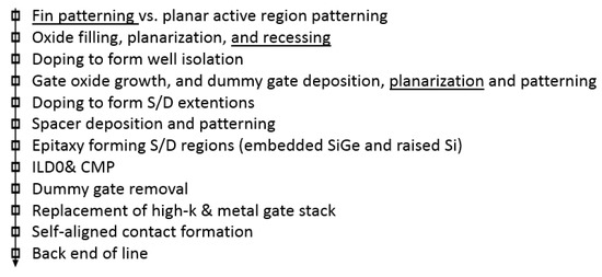
Figure 1.
Process flow for the bulk fin field effect transistors (FinFETs) or planar transistors where additional processes for FinFETs are underlined.
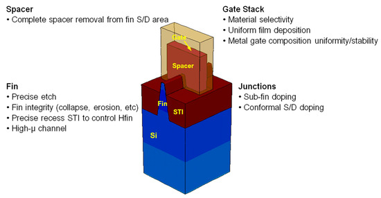
Figure 2.
New challenges in fabrication of FinFETs.
3.1. Precise and Uniform Fin Formation
Electrical characteristics of FinFETs are closely correlated to the fin profile (width, height, and verticality) [25]. To handle more current, longer fins are needed which results in more challenges to manufacturing. Smaller fin width is favorable to channel electrostatic control, but this design cannot go too far, because of mobility degradation, random doping fluctuation (RDF) from the S/D gradients, and variation in off-state current.
Fins are usually defined by SADP [26]. Fin etching in bulk silicon has to be controlled by a timer process. In the most cases, the fins at the edges of a cluster suffer a higher variability than those in the middle. To achieve uniform fin width and height in a cluster, dummy fins are required [27]. Some dummy fins need to be cut at the pitch. As fin pitch shrinks and approaches the overlay limit, cutting fins becomes more difficult. Fin isolation by STI and channel-stopper doping step are also challenging, because of the tighter pitch, difficulty to control on STI depth, and doping variation.
To preserve structural integrity of fins with a high aspect ratio is also another challenge. The Si surface of narrow fins appears differently than Si bulk [28], and excessive Si loss was observed after the usual wet cleaning. Thus, wet process needs optimization with a diluted concentration and a lower temperature. Similarly, the oxidation is also faster at corner and tip of fins. Furthermore, the dry etching of fins is more stringent due to the 3D topography, therefore, a plasma pulsing scheme may be viable for minimizing Si loss [25]. The growth of defect-free alternated fin materials for high mobility channel application is also a challenge due to differences in thermal budget and lattice matching [27].
3.2. 3D Gate and Spacer Patterning
To form long fins increases the complexity of integration of poly gate, spacer, and replacement metal gate. For example, it is difficult to etch the poly gate with high aspect ratio and precise control of dimensions [25]. Charging and micro-loading in etching lead to variable gate length (Lg). Significant over-etch is required to clear the poly residual on the fin sidewalls, and significant over-etch is also required to clear the offset spacers on the fin sidewalls for epitaxial S/D growth [28,29]. Both these over etchings results in damages of the Si fins. Careful optimization of dry and wet etching is needed to produce 3D gates with minimum Lg variation and fin loss.
The replacement metal gate module also poses challenges, as it requires two new steps which can interact during the STI CMP. The control of gate height is essential in a replacement gate process. If the gate is over-polished, the raised source-drain is exposed to the polish, resulting in external resistance (Rext) and mobility variation. Meanwhile, when the gate is under-polished, the contact taper causes Rext variation (in extreme case resulting in an open-contact yield issue). Therefore, more precise and more controllable CMP process is required [30].
3.3. Uniform Junction Formation in Fin
One of the critical integration challenges for FinFETs lies with doping, which in fins is significantly different than that in planar devices [31,32]. Three issues are included: (1) the need for conformal doping in the S/D contact and extension regions so that the carrier conduction is uniform in the fin-channel; (2) the tight pitch of the fins limits the beam incidence angles, then the shadowing from neighboring fins has be avoided; (3) damage, accumulation and annealing in high-aspect ratio fins are significantly different from those in planar junctions.
Uniformly doping with conventional ion implantations in the narrow and long fins with a shrunk pitch is a difficult task (I/I) [33]. After conventional I/I, an amorphization of the Si fins occurs and later poor re-crystallization is obtained during junction anneal which results in poor dopant activation and defected fins [31]. The implant condition for fin doping can also impact the quality and the growth rate of the S/D epitaxy, which will have implications on the S/D and contact resistance. Hot I/I with increasing the Si wafer temperature during I/I up to a certain targeted value could be an option to reduce the amorphous depth and fin damage [31,32]. Other innovative doping schemes e.g., solid-source doping, conformal plasma doping, and molecular monolayer doping can be also applied to improve the doping profile. An extension less and I/I-free doping technique is preferably required, which uses rapid thermal annealing (RTA) process to drive dopants from the in situ doped epitaxial S/D regions, and to form a better controlled box-shaped profile.
3.4. Stress Engineering
Stress engineering is a crucial issue for Si MOSFETs. There are three commonly used methods for stress engineering in nano-scaled transistors e.g., stress memorization technique (SMT), SiN contact etch stop layers (CESL) stressors and epitaxy of SiGe on S/D regions are used to create stress in the channel region. Among these methods SMT and CESL are less effective for FinFETs and nano-wire FETs.
SMT is grounded on growth of a highly tensile-stressed SiN followed by a thermal annealing step >1000 °C. In this process, the SiN capping layer is deposited on the whole Si wafer and it is kept on the n-type metal oxide semiconductor (nMOS) region while it is selectively removed from the p-type metal oxide semiconductor (pMOS) area. Stress is mainly memorized during the anneal step for activation step in S/D areas. A wet etching is applied after SMT process to remove the SiN layer before silicide formation.
In SMT, the stress memorization is originated from compressive stress which is induced by the n-type poly-Si gate under the SiN capping layer. The volume of polycrystalline material expands during the annealing step and induces a tensile stress along the longitudinal direction, as shown in Figure 3.
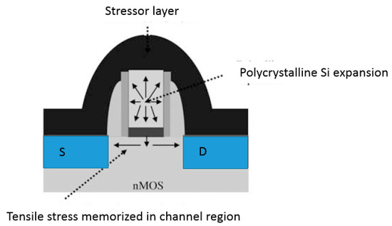
Figure 3.
Schematic of stress memorization technique (SMT) in n-type metal oxide semiconductor (nMOS) with a stressor cap layer.
A more innovative way to induce stress in planar transistors is CESL. This technique consists of a SiNx layer deposited around the gate stack as shown in Figure 4. By tuning the process parameters the stress amount and its type: tensile or compressive can be determined [34].
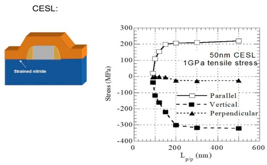
Figure 4.
Schematic illustration of a contact etch stop layers (CESL) cap layer for implementing for example parallel tensile stress in a planar n-MOS. The different strain components, as determined by technology computer aided design (TCAD) simulations are shown in the right diagram as a function of the transistor pith Lp/p.
The most effective method to induce stress in S/D is embedded SiGe (compressive stress for pMOS), Si:C (tensile stress for nMOS) or trench contact, and in metal gate [34]. More aggressive scaled nodes have tighter contacted poly pitch (CPP), resulting in less room for gate and S/D. Effectiveness of the gate and S/D stressors depends on the trade-off between reducing stressor volume and enhancing stressor proximity to channel [35].
To further enhance the channel mobility in planar MOSFETs, the Ge content in SiGe S/D has been continuously increased from 17% to 40% in 90 nm to 22 nm node, respectively [36,37,38,39,40]. Further strain could be induced when the shape of recessed S/D changed from a round shape to sigma (Σ) shape where the SiGe layers locate deeper in the channel region as shown in Figure 5 [41,42,43].
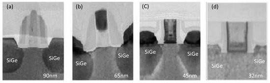
Figure 5.
The evolution of nano-scaled transistors having SiGe as stressor material in source/drain (S/D) for each node (a) 90 nm, (b) 65 nm, (c) 45 nm, and (d) 32 nm. Sigma shape recess was introduced for the first time in 45 nm. Reproduced with permission from [44]. Copyright SPIE, 2016.
The evolution of Ge content in S/D and stress created in channel for different technology nodes is shown in Figure 6. The 3D architecture was designed and manufactured for 22 nm node. SiGe layers are selectively grown by reduced pressure chemical vapor deposition (RPCVD) technique by using SiH2Cl2, GeH4 as Ge and Si precursor, respectively. During epitaxy, HCl gas is introduced for etching the formed nuclei on the SiO2 surface to ensure the selectivity of the growth.
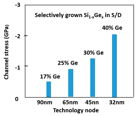
Figure 6.
The evolution of Ge content in SiGe S/D and stress created in channel for different technology nodes.
The epi-layers may suffer from several problems e.g., facet formation [44,45], defects, micro/loading, non-uniform strain distribution, surface roughness and pattern dependency effect [46,47,48,49,50]. The pattern dependency happens when the density and size of the transistor vary in a chip. The reason for the pattern dependency of selective epitaxy is mainly non-uniform consumption of reactant gas molecules when the exposed Si area varies in chip. This problem can be decreased by optimizing the growth parameters (high HCl partial pressure, low total pressure and high hydrogen carrier gas pressure) and by designing chip layouts where the exposed Si is uniformly distributed over the chip’s area to create uniform gas consumption [50].
The big challenge when the planar transistors are redesigned to 3D is uniformity of strain and the control of the defect density in the channel region. Figure 7 shows how the epitaxy occurs for planar and 3D transistors. The precursor molecules are piloted by hydrogen over the wafer and moves forwards along the chemical vapor deposition (CVD) quartz. A gas boundary is established over the wafer where the molecules may diffuse downwards (according to Fick’s diffusion equation). Later these molecules are attracted within a spherical volume towards the dangling bonds which are available sites in the exposed Si areas of the chips.
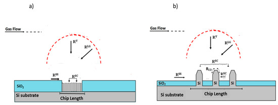
Figure 7.
Schematic view of gas flow in different directions over a chip containing (a) planar transistors and (b) FinFETs. The dashed circles (sphere in 3D) representing a volume where the molecules around the transistor arrays (or chips) are attracted.
The total growth rate (RTot) consists of components from vertical (RV) and lateral (RLG gas flow, as well as components from oxide surface around the transistor arrays (Rss) and oxide surface between the transistor openings (RSC) for SiH2Cl2, GeH4 and HCl gases. Thus, RTot for SiGe growth in planar transistors is written as [50]:
The above equation can be modified to estimate the growth rate of SiGe on Si fins in 3D FinFETs (elevated S/D) when an extra component (RCO) is added. This component is rooted from the diffusion of molecules on the surface of Si fins. Then Equation (1) is written as [51]:
The RCO component makes a unique situation for the growth of 3D transistors when the molecules can move from a fin to another one creating a more uniform growth.
It is worth mentioning here that the components RSS and RSC are changed if the chip layout is changed. These components which are layout-dependent are the cause for pattern dependency in selective epitaxy growth.
3.5. Stress Measurements in Nano-Scaled Transistors
The stress in nano-scaled transistors can be measured by Nano-beam diffraction (NBD) technique in high-resolution transmission electron microscope (HRTEM). The diffraction pattern from the selected areas varies depending on the stress amount and the analysis can be performed in combination with True Crystal program package. In NBD analysis, the interplanar distance of (220) planes is measured and later compared by the calculated data. Afterwards, the stress amount (ε) is transformed into the strain (σ) by using the relationship: ε = σ/E where E is Young’s Modulus.
As an example, Figure 8 illustrates the NBD images from a 22 nm planar transistor with atomic layer deposition tungsten (ALD W) metal gate formed by B2H6 doping source. The analysis was performed by a nano beam on the metal gate, channel and the body regions of a transistor. The diffraction images from the metal gate materials illustrate a pattern with weak intensity which is a sign of poor polycrystalline or likely an amorphous phase. The strain in the channel region is estimated to ~0.5 GPa [52].
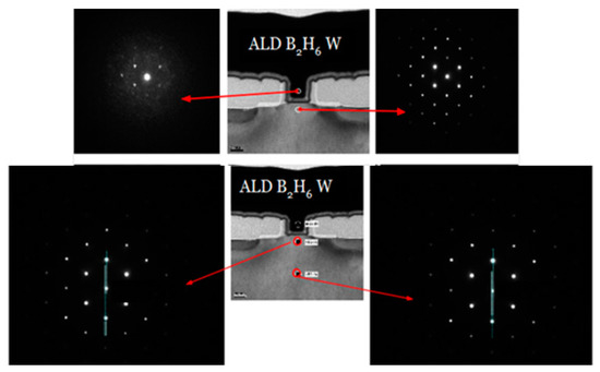
Figure 8.
Nano-beam diffraction (NBD) micrographs from metal gate, channel and the body regions of a 22 nm planar transistor [52].
It is important to note that a careful sample preparation is necessary since the stress may partially relax during the ion milling or any other mechanical force. This problem becomes a real challenge to prepare 3D FinFET samples for strain analysis by HRTEM.
Another method to measure stress (or strain) is X-ray diffraction (XRD). This technique applies scanning of incident beam (ω angle) and the detector follows to detect the diffracted beam (angle 2θ) in a configuration so called ω−2θ rocking curve (RC) scans. The Si substrate and SiGe layer satisfy the Bragg law condition for a certain ω and 2θ resulting in peaks [53]. The strain can be determined from the split of the peaks. A more accurate strain measurement can be performed by using high-resolution reciprocal lattice map (HRRLM) where the misfit in-parallel and perpendicular to the growth direction (f// and f⊥, respectively) can be obtained. The position of Si and SiGe peaks in the reciprocal space are the parameters which are obtained from HRRLMs and are used to calculate the misfit parameters. Due to a limited X-ray spot size the strain measurements provide a mean value over an array of transistors rather than individual transistor compared to HRTEM analysis [54].
HRRLMs have been widely used to determine the boron concentration in SiGe or Si as well as strain relaxation in process line [54,55]. The analysis can reveal the formation of silicides in S/D regions (for the reducing contact resistance) results in strain relaxation in SiGe layers [56]. This is because of the silicide formation generates significant amount of point defects during the consumption of Si atoms. During the silicide formation, the Ge atoms diffuse out and create a SiGe layer with rich Ge content beneath the silicide layer. As a consequence, the strain in SiGe beneath the silicide layer partially relaxes. A remedy to this problem is the growth of a Si sacrificial layer [57].
As an example, Figure 9a–c show three HRRLMs around (113) reflection from chips containing arrays of 22 nm planar transistors with intrinsic Si0.65Ge0.35, B-doped Si0.65Ge0.35 and B-doped Si0.65Ge0.35/NiSiGe in S/D regions, respectively [49]. The silicide layer has been formed on a sacrificial SiGe layer with lower Ge content (20%). In Figure 9a, both Si and SiGe peaks are aligned along K⊥ direction showing a minor strain relaxation in SiGe layer. Meanwhile, in Figure 9b, there is a shift of B-doped SiGe peak compared to intrinsic ones in Figure 9a. This shift is due to strain compensation in presence of B atoms in Si matrix and it corresponds to the number of substitutional boron concentration. By applying the contraction coefficient of boron in Si ((6.3 ± 0.1) × 10−24 cm3/atom) and the amount of the strain compensation, the boron concentration is estimated to 2 × 1020 cm−3.
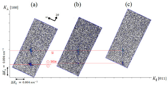
Figure 9.
high-resolution reciprocal lattice maps (HRRLMs) around (113) reflection from 22 nm metal oxide field effect transistors (MOSFETs) with Si0.65Ge0.35 in S/D areas as follows (a) an intrinsic layer and (b) B-doped layer (c) as previous sample but with a SiGe sacrificial layer which was consumed in NiSiGe cap layer. Reproduced with permission from [54]. Copyright Journal of Applied Physics, 2013.
Further investigations about the effect of NiSiGe formation on the SiGe strain were performed. In Figure 9c, the SiGe peak is at the same position as in Figure 4b indicating the strain in SiGe is preserved during the Ni silicide formation process [49].
Although HRRLMs is a powerful technique for strain measurement and they can be easily obtained by conventional high-resolution X-ray apparatus, they cannot measure strain in ultra-small SiGe crystals grown on Si fins in 3D FinFETs due to the limited signal acquisition. Therefore, the strain amount in the processed FinFET structures was determined by using X-ray beam in a Synchrotron facility as shown in Figure 10 [50]. The high intensity beam offers the chance to determine the misfit parameters and the strain relaxation condition for small SiGe crystals. In Figure 10, the SiGe peak is aligned with Si peak along K⊥ indicating a small strain relaxation amount.
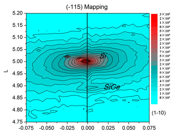
Figure 10.
HRRLM at (−115) reflection from 14 nm FinFETs arrays with of SiGe in S/D areas. Reproduced with permission from [50]. Copyright Solid-State Electron, 2016.
3.6. High-k Dielectric and Metal Gate (HKMG)
In order to satisfy the aggressive down-scaling of metal oxide semiconductor (MOS) transistors a large effort was devoted to use new gate materials to solve the unendurable integrating problems involved in producing chips [58,59,60,61]. Therefore, both new high-k gate dielectric and metal gate electrode materials were sought. The exploration for new high-k dielectrics was focused on resolving boron penetration and polysilicon depletion issues. The other important concern was also compatibility of high-k dielectrics with new metal electrodes which were required to replace the traditional polysilicon gate electrode used in nMOS and pMOS transistors [62,63,64].
In this part, the material choice of high-k dielectric and metal gate for different technology nodes are presented and then atomic layer deposition (ALD) of metal gate, which is the main challenge beyond 14 nm technology node due to the much high aspect ratio is discussed.
3.6.1. Evolution of HKMG
New high-k dielectric and metal gate were initially introduced into 45 nm technology node MOSFET by Intel Corporation at 2007 [65]. Table 3 summarizes the evolution of high-k dielectric and metal gate from 45 nm to 14 nm nodes. It can be seen that the HfO2 is used as gate dielectric for both nMOS and pMOS. The HfO2 high-k dielectric has high permittivity (a dielectric constant about 25 and a relatively large bandgap, 5.7 eV), large heat of formation (−271 kcal/mol, higher than that of SiO2: −218 kcal/mol), good thermal and chemical stability on silicon, large barrier heights at interfaces with Si, and adequate compatibility with n+ poly-silicon gate electrodes. At an operation voltage of 1–1.5 V, the leakage current through HfO2 dielectric films was reported to be several orders of magnitude lower than that of SiO2 with the same EOT (0.9–2 nm) [39,65]. One of the main challenges of HfO2 application in CMOS technology is the thermal instability of HfO2/Si contact. There is an inevitable interlayer such as SiOx between HfO2 and Si substrate [65,66,67], even though the HfO2/Si is theoretically found to be thermodynamically stable [68]. Table 3 summarizes information about different materials as high-k dielectric and metal gate from 45 nm to 14 nm technology node. The table also shows that TiAlN and TiN are applied as metal gates for nMOS and pMOS, respectively.
Table 3.
Material selection of high-k dielectric and metal gate from 45 nm to 14 nm nodes.
The other important point is that the thickness of gate dielectrics is changed, although the same dielectric materials are used. As shown in Table 4, the thickness of thermal oxide (SiOx) has been reduced dramatically from ~1.2 nm in 45 nm node to ~0.7 nm in 14 nm node. In similar manner, the high-k dielectric decreases from ~1.5 nm in 45 nm node to ~1.2 nm in 14 nm node. As a result, the equivalent oxide thickness of gate dielectric has been decreased.
Table 4.
Key parameters of high-k dielectric and metal gate from 45 nm to 14 nm nodes.
3.6.2. Atomic Layer Deposition of Metal Gate
Continued scaling down of CMOS devices requires high-k dielectrics and metal electrodes to replace traditional SiO2 dielectrics and poly-silicon gate electrodes [69,70]. The replacement of poly-silicon with metal gate is essential in order to prevent the Fermi level pinning effect and poly-silicon depletion [71,72]. Intel introduced TiAlN and TiN are used as work function metals for nMOS and pMOS, respectively for 45 nm and 32 nm node [39,40]. With further down scaling of the CMOS device into 22 nm node and beyond, a three-dimensional FinFET structure was introduced into the CMOS in order to suppress the short-channel effects [21]. In such transistors, the aspect ratio of the replacement gate structure became larger, and this made it difficult to fill the trench.
Atomic layer deposition (ALD) is widely regarded as the best solution for metal gate deposition because of its excellent conformal step coverage capability [73,74].
The metal gate materials such as TiN, TiAlN, HfAlC, TaN, HfN, AlN, TiCxNy, TiC-TiN have effective work function of 4.6–5.0 eV, which can be used in pMOS or SOI device [75,76,77,78]. Jeon and Park et al. synthesized a thermally stable triple Ti1−xAlxN metal gate and studied the effect of Al concentrations in the atomic-layer-deposited Ti1−xAlxN layers on the effective work function. Tunable effective work function of 4.86–5.04 eV was measured which could be implemented for pMOS [76]. Recently, the impact of using ALD technique on the effective work function of carbon-containing TiN films (TiC–TiN) has been presented. The results demonstrated that the bonding concentration of Ti–C increases at higher deposition temperatures and in contrast the work function of the TiC–TiN metal gate decreases from 5.0 to 4.6 eV.
A high work function of 5.0 eV metal gate is suitable for a p-FET application while the midgap work function 4.6 eV is suitable for a fully depleted silicon-on-insulator FET [75]. ALD HfxAlyCz films using hafnium chloride and trimethylaluminum precursors were studied by Lee et al. [77]. The effective work function in metal–oxide–semiconductor capacitor devices with the HfxAlyCz layer was quantified to be 4.6 eV which is compatible with an ALD HfO2 dielectric. Thus, HfxAlyCz is a metal gate work function material that can be used for the tuning of device threshold voltages (Vth) for anticipated multi-Vth IC devices [78].
For nMOS, due to the lack of appropriate precursor, it is relatively difficult to acquire n-type work function metal. Ragnarsson et al. applied a new ALD TiAl process to demonstrate conformal low Vth bulk FinFET devices [79]. Cho et al. used tert-butylimido tri-diethylamido tantalum and methane/hydrogen reactive gas mixture to obtain ALD TaCxNy films. By introducing of 1.5–2.5% methane, the TaCxNy film with lower work function could be obtained. For these films, the lowest effective work function of 4.37 eV could be achieved [80]. Triyoso et al. introduced TaCy film deposited by plasma-enhanced ALD (PEALD) technique to extend the effective work function within 4.54–4.77 eV [81].
For the metal gate, the thermal ALD without plasma damage is more suitable. Chao et al. developed TiAlX films as metal gate by thermal ALD technique using titanium tetrachloride (TiCl4), trimethylaluminum (TMA) and NH3. It was demonstrated that NH3 presence in the TiCl4 and TMA reaction resulted in the film more like TiAlN(C) while its absence made the film turn to TiAlC. The TiAlC films have smaller effective work function than the TiAlN(C) films [82]. The effective work function can be tunable from 4.49 eV to 4.79 eV by tuning growth temperature, TMA dose and film thickness [83]. Further studies showed that the effective work function of TiAlC films can be decreased by increasing Al concentration. Chao et al. introduced a new precursor triethylaluminum (TEA) to react with TiCl4. TEA is a metal organic precursor with special β-hydrogen, which can lead to H2 elimination. The H2 elimination will generate Al intermediate, which can decompose more easily at high temperatures and further enhance Al doping into the final product [84]. The effective work function of the TiAlC with TEA as precursor can be tunable from 4.46 eV to 4.24 eV by adjusting the growth temperature and the film thickness. TaAlC based on TMA and TEA has almost the same effective work function as TiAlC based on TMA and TEA separately [85,86].
However, for filling metal in the transistor dummy gate trench, W metal using ALD has a good capability of step coverage to instead traditional physical vapor deposition (PVD) Al materials applied in the small pitch device. There are two types of ALD W films depending on SiH4 and B2H6 precursors. The related research showed that the properties of the ALD W were precursor-dependent due to crystalline quality and induced strain of the deposited films [87,88,89].
3.7. Additional Sources of Variation
Variability control is more critical and becomes increasingly challenging for FinFETs [90,91]. FinFET’s electrical variation is very sensitive to fin width and verticality variations. Fin height variation comes from fin etching, STI deposition, STI CMP, and STI recessing.
In general, gate etching profile and Lg variation over fin topography are difficult to control. S/D epitaxy is a sensitive process over fin topography [92] and the resistance and stress fluctuations may be resulted if the fin shape is affected. Furthermore, in I/I process, the defected layers would correspond to another source of variability [91]. In a fin with channel doping concentration of 6 × 1017 cm−3, about a third of the variability comes from random dopant fluctuation (RDF). While channel doping can be avoided in FinFETs, RDF from S/D doping gradient appears when Lg < 10 nm [33,93]. Channel interface and gate stack work function variations have remarkable negative effect on the transistor performance. Double patterning raises concerns about the way in which individual polygons are split across two masks. As overlay is not scaling as fast as minimum feature size, mask-alignment issues introduce a new source of variability in the spacing between polygons [27].
3.8. Common Challenges: Less Lateral Space Left
Continuous scaling suggests endless reduction of CPP. This results in a trade-off between Lg, S/D spacer thickness, and S/D contact area in a lateral device. Lg is limited by short-channel effects. Minimum spacer thickness is defined by reliability requirements and/or by capacitance between gate and S/D electrodes. Narrow S/D contacts result in high access resistance.
Gate-all-around (GAA) FETs offer the best potential solution to electrostatic control, and can be implemented in a lateral (with one or more lateral wires which are vertically stacked) [94,95] or a vertical configuration [96,97]. The lateral nanowire FETs are closer to FinFETs in terms of processing, circuit design, as well as footprint constraints. The vertical nanowire FETs are less constrained on Lg, spacer thickness, and S/D contact area, as they are oriented vertically and thus should possess even better scalability [96,97]. However, the move towards a vertical architecture will require more disruptive technology and design changes to be considered and implemented.
Down scaling has always acted against wiring performance. At and below 22 nm, interconnect resistance is set to rise dramatically. Besides the wire cross-section reduction, carrier scattering from the boundaries of individual copper crystal grains, and interfaces with barrier layers are rapidly pushing up interconnect resistivity and the resistance of individual wires. Double patterning also leads to routing challenges, and the access to standard cell pins is more difficult because of constraints on interconnect pitch. Interconnect resistance and capacitance (RC) starts to dominate the delay. The line/via resistance and capacitance need to reduce, while reliability (electromigration (EM), time dependent dielectric breakdown (TDDB), bias temperature instability (BTI) and hot carrier injection (HCI)) needs to be maintained. Before these, defect-free metal filling is a prerequisite. However, reducing line resistance needs enough space for actual wiring material, leaving less room for barrier and thus poor reliability like EM. Lower via resistance needs thinner barrier at via bottom causing EM blocking boundary insufficient [98].
4. Dopant Implantation in CMOS
For decades, Ion implantation has been a major doping strategy for a planar CMOS device in S/D formation or threshold voltage adjustment. However, when the transistor dimension shrunk below 100 nm the extended S/D implantation needed to be more aggressive to inhibit the short channel effect [99]. In MOSFETs, shallow junction (USJ) was sought to follow the down-scaling geometrical rules.
Initially, USJ was realized by low ion implant energy and followed by a traditional rapid thermal process (RTP or spike annealing). A series of low energy high current ion implanter were also developed to improve the throughput of the tools [100,101]. While the gate length was further scaled to 45 nm node and beyond, the transient enhanced diffusion (TED) effect of the dopant was more and more apparent and a desired junction depth (International Semiconductor Technology Development Roadmap(ITRS) required) could not be achieved by just low energy implantation. Some novel solutions e.g., co-implantation, cryogenic implantation or Cluster implant were developed to reduce the dopant’s diffusion in the substrate during activation step [102,103,104,105,106]. For co-implantation, carbon was proved to be an appropriate species with good control of dopant diffusion in both silicon or germanium based transistors [107,108].
On the other hand, the annealing technology was also improved e.g., laser anneal and flash anneal can activate the dopant within milliseconds [109,110]. These techniques can not only reduce the thermal budget of the annealing process, but also improve the activation level of the dopant. Nowadays, these techniques have been used as standard source/drain thermal treatment in CMOS fabrication. In recent years, a new thermal treatment method so-called microwave annealing is found to be useful for shallow junction formation. This technique offers the annealing process at rather low temperatures with less dopant diffusion [107,111]. Since the temperature of activation is lower than 500 °C, it could be meaningful for Ge based devices in future.
4.1. Challenge of Ion Implantation in 3D Structure Devices
In 2012, 3D tri-gate transistors came into mass production by Intel on its 22 nm micro-processor. Such a design brings a lower junction leakage and better short channel effect control compared to traditional planar structure. However, in the meantime, the transformation from planar to 3D put forward higher requirements for the fabrication process such as implantation, the conformal doping of source/drain areas and lower fin damage by implantation [112].
4.1.1. Conformal Doping
For 3D structure devices like FinFETs, the requirement for S/D extension is not limited for highly dopant activation or less dopant diffusion and profile abruptness, but the conformal distribution within the fins [112,113,114]. The non-conformal doping profile results in degradation of the drive current of the transistor. Although large tilt beamline implantation could improve the conformality but there is still a serious limitation on the tilt angle due to shadowing by the neighboring fins.
An alternative approach to improve conformality is using plasma doping [115,116,117]. The fins were immersed into plasma where the top surface and sidewall of the fins could be conformally doped by appropriate atoms. However, in order to prevent the dopants out-diffusion from the surface and make a better doping uniformity, a capping layer is always deposited before activation annealing.
4.1.2. Damage Control
The damage control during doping is another key point to promote the performance of device. In planar devices, low temperature cryogenic implant is used to eliminate the end of range defects, while for 3D FinFET structure, the situation is quite different. It was found that a narrow fin which is isolated from large crystal volume; surface proximity and the 3D structure make amorphous silicon recrystallization problematic. If the fin is completely amorphized, only a very small seed for recrystallization, which results in a defective growth, and it degrades the resistivity and drive current of the transistors [118,119]. Therefore, for 3D transistors, it is necessary to reduce the amorphization depth created by implantation as well as the annealing to minimize the fin damage.
Hot implantation is proved to be a solution for damage-free fin source and drain extension (SDE) doping. By increasing the implantation temperature, damage accumulation could be mitigated, thus the self-amorphization of implant can also be decreased. By using this method, B. Wood et al. demonstrated a half magnitude improvement in fin line conductance and one magnitude in junction leakage for n-type source and drain extension (NSDE) doping compared to a room-temperature implant [120].
5. The Etching Challenges and Solution of 3D
5.1. Depth Loading Control of Fin Etching
Generally, only a small part of process gases is ionized into plasma under the radio frequency power. Most of molecules exist in the chamber as neutrals, which induce deposition during etching process. Neutrals are easy to stick on to the surfaces before entering trench bottom and they induce taper profile that will block ions to reach to the bottom. On the other side, new stored ions are formed at trench bottom to react upon the incoming ions. As a result, as etching reaction is on going and etching depth increases, flux ratio of Ion/Neutral will decrease and etching bombardment is weakened as shown in Figure 11a. Within CD sizes, smaller CD induced weaker bottom reaction. Therefore, the etching depth depends on the opening CD size: bigger opening CD size induce deeper depth as shown in Figure 11b.
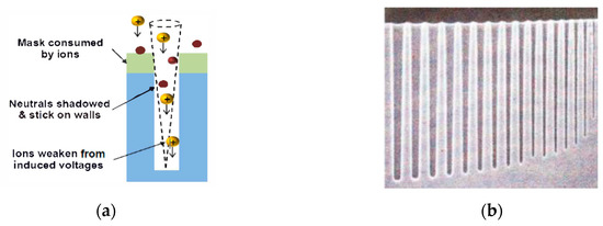
Figure 11.
(a) Depth reduced Ion/Neutral flux ratio and (b) Opening CD size dominates the depth loading. Reproduced with permission from [121]. Copyright IEEE, 2015.
It is possible to fine-tune the gas ratio and bias power to improve the Ion/Neutral flux ratio and improve the CD size dependency to etch rate. However, this traditional tuning is less effective to 14 nm FinFET due to the extreme small size limit the function and cannot meet the requirement of 5 nm depth loading. Using higher bias power will induce higher electron temperature that will damage under layer in gate or spacer etching process. To solve this problem, the concept of bias pulsing can be introduced. Since bias power is the main source to provide ion bombardment, bias pulsing can change Ion/Neutral flux ratio momentarily as bias power turn on/off. However, the flux ratio at bias-on is greater than that at bias-off. Figure 12a,b shows how the bias pulsing affects the etching process during both bias-on and bias-off. When the bias power is on, plasma etching dominates the process. While the neutral deposition dominates during the bias-off. In bias opening moments, ions may crush the bottom of trench in a short time and react with silicon in the bottom. In this case, when the bias power is turned off suddenly, it will induce enough reacting before the back potential force forms. This kind of time-split to bias on/off results smaller depth loading effect that are caused by different opening CD size [122,123].
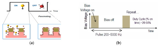
Figure 12.
(a) Bias pulsing power effect and (b) Bias pulsing process. Reproduced with permission from [121]. Copyright IEEE, 2015.
For example, using bias power pulsing, the intra-cell loading can be reduced from 20 nm to 5 nm under 5 nm CD difference structure as shown in Figure 13.
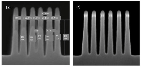
Figure 13.
Bias pulsing improve intra-cell depth loading (a) loading without pulsing and (b) loading with pulsing. Reproduced with permission from [121]. Copyright IEEE, 2015.
5.2. Gate Etching Control
As new 3D structures are introduced, selective and residue-free etch processes will be even more challenging. There are a few new process and materials challenges in processing FinFETs as summarized below. Firstly, the Si surface of fins appears different than in bulk since an excessive Si loss was observed after the usual pre-gate-oxide clean as shown in Figure 14a. Therefore, wet cleaning was optimized with dilute concentration and lower temperatures. Similarly, the oxidation of fin is also faster at corner and tip of fins. Furthermore, the dry etching on fins is more stringent due to the 3D structures (Figure 14b) and a bias plasma pulsing scheme may be viable for minimizing Si loss [124,125].
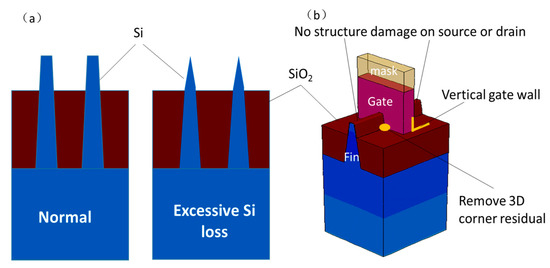
Figure 14.
(a) The Si-loss of fins appears more severe than bulk and (b) the plasma etching is more difficult on 3D structures.
Self-Aligned Contact (SAC) Etching Selectivity Control
In general, SAC is a necessary process for 3D transistor with gate length smaller than 14 nm. It is required to etch the slit pattern of the fine SiO2 layer with ultra-high selectivity to SiN. In the conventional etching methods which fluorocarbon (FC) gas is usually used, the selectivity is enhanced by utilizing the etch rate difference of the protective film, which is caused by the composition difference of SiO2 and SiN [126,127]. However, if the FC film thickness is increased in attempt to improve the SiN selectivity, an excessive FC film is deposited on SiO2 and the slit opening is blocked by excess deposition where finally it causes an etch-stop to occur. Therefore, a better trade-off between the fine process control of the SiO2 layer and SiN selectivity can be reached by applying a new Quasi-Atomic Layer Etch (ALE) technology [128].
Figure 15 shows the concept of Quasi-ALE. In the conventional method, radicals and ions in the plasma are transported to the surface of wafer at the same time. In contrast, in Quasi-ALE, they are separated as the radical flux and ion flux are performed independently in each step time. In this scheme, it is possible to control the etching reaction more precisely.
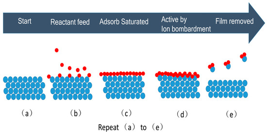
Figure 15.
The concept of Quasi-ALE with (a) process started; (b) reactant feed deposited; (c) adsorb saturated; (d) active by Ion bombardment and (e) film removed.
Figure 16 shows the etching result of SAC structure by the conventional etch and optimized Quasi-ALE. In the conventional etch, etch stop occurs at the fine slit while the amount of SiN loss is large. In Quasi-ALE, the fine slit can be successfully etched while the SiN selectivity is highly preserved. SEM image of Quasi-ALE shows when FC on the bottom of fine slit has been removed but the SiN surface is still protected by FC layer. From the state of the FC layer formation, precise control ability of the etching surface by Quasi-ALE is obtained. Thus, Quasi-ALE enables very sophisticated fabrication.
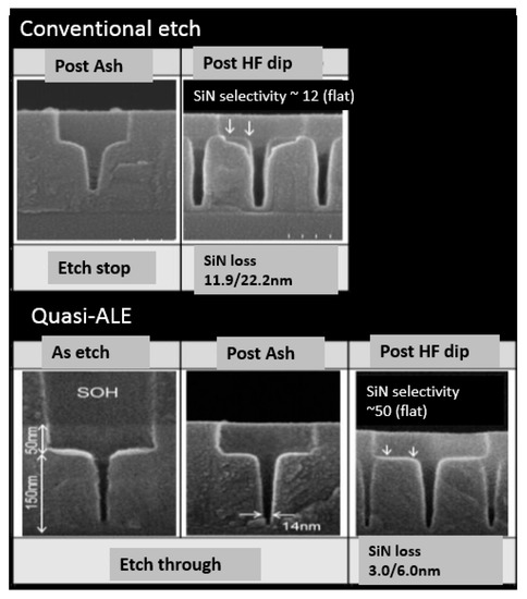
Figure 16.
Cross-section SEM images of self-aligned contact (SAC) structure after the conventional etch and optimized Quasi-ALE. Reproduced with permission from [128]. Copyright IEEE, 2016.
5.3. STI Process for the Gate
The STI process of Si fins is described in Figure 17 [129]. One of the critical processes is to control the fin height (Hfin) since it has influence on the electrical properties of transistors, e.g., the threshold voltage (Vth) decreases as Hfin decreases . In order to etch silicon dioxide, hydrogen fluoride acid (HF) based reagent is used. However, wet etching normally causes footing due to its isotropic etching nature as shown Figure 18a,b [130]. In any case, high temperature annealing has to be avoided to prevent the material inter-diffusion but low temperature processing leaves low quality of STI oxide [4,130].
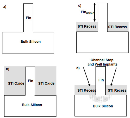
Figure 17.
A schematic of STI process of Si fins with (a) Si fins formation; (b) STI oxide filled in; (c) STI oxide recess and (d) channel stop and well implants. Reproduced with permission from [129]. Copyright Springer, 2008.
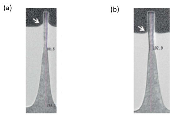
Figure 18.
STI footing by wet etching with (a) an oxide foot at the bottom edge and (b) footing is reduced and recess control is improved due to digital nature of the etching. Reproduced with permission from [130]. Copyright Solid-State Electronics, 2012.
In general, the lower quality of oxide, the higher etch rate (ER) is anticipated. The method to moderate the elevated ER for better process control is to either reduce the concentration of the main species or to decrease the etching time. Normally, the former has better process window compared to the latter.
5.4. Gate Process
The replacement metal gate (RMG) was introduced by using poly-Si as dummy gate and SiO2 as dummy gate oxide [131] where eventually these layers are removed with wet process by means of none metal alkaine solutions, as shown in Figure 19 [132,133,134]. One of benefits of RMG is to avoid crystallization of the high-k dielectric during the rapid thermal annealing (RTA) process for dopants activation [135]. The other important benefit is the chemical reaction between the metal gate and the high-k in RTA processes is also avoided otherwise the boron diffusion into high-k is inevitable. As an example, the boron diffusion for HfO2 is significant higher than SiO2 [135,136].
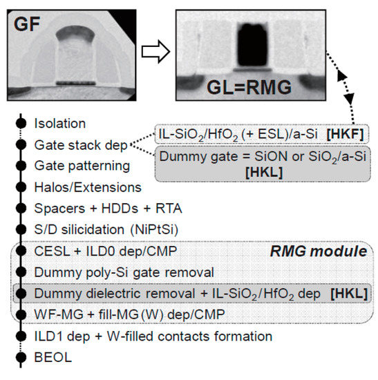
Figure 19.
Planar transistors with high-k metal gate processes, including replacement metal gate (RMG) modules. (Reprinted with permission from [3]. Copyright Japan Society of Applied Physics, 2011).
Compared to the 2D devices, the RMG for 3D structures are even more complicated as shown for vertically stacked nanowire process in Figure 20. Firstly, poly-Si dummy gate has to be completely removed without any residues in narrow and steep trenches [132,133,134], otherwise, due to chemical nature of the HF-based wet etchant for the dummy gate oxide etching could not remove the poly-Si without any oxidizer [137,138,139]. Therefore, the residues occupy the space where the high-k and metal gates should be filled in, which might cause device failure. Besides this problem, a careful selective etching process is required to create dangling structures, for example in the vertically stacked nanowires [130]. In general, the wet processes use aqueous solutions which are using water as the solvent, and the final rinses are using deionized water (DIW) or ultra-pure water (UPW) to clean away the chemicals from wafer surfaces. However, it is well known that some defects can be generated due to the surface tension of water. Normally, during the drying process, the high capillary force of water could pull nearby structures to form permanent defects so called pattern collapse [140] or stiction [141] in terms of micro electro-mechanical systems (MEMS) field. To avoid such defects, gas phase etching (GPE) was carefully studied in the latest decades. In gas phase, the intermolecular force is not too strong compared to the liquid phase, then there is no worry about any pattern collapse. Besides that, the diffusivities in gases are 104 time greater than in a liquid. The commonly used GPE is a HF vapor process. Recently, GAA transistors have been manufactured by using HCl vapor process as well [130,131,132,133,134,135,136,137,138,139,140,141,142].
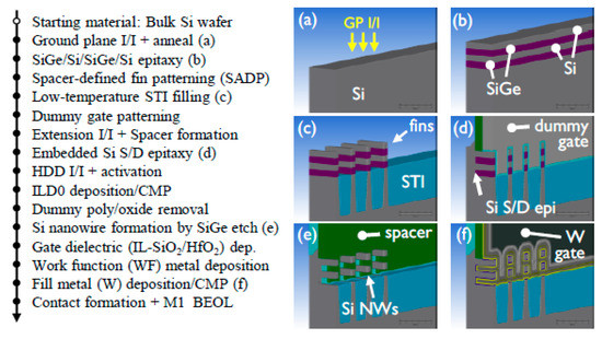
Figure 20.
Vertically stacked nanowire process flow including RMG modules. (a) Ground plane I/I + anneal; (b) SiGe/Si/SiGe/Si epitaxy; (c) Low-temperature STI filling; (d) Embedded Si S/D epitaxy; (e) Si nanowire formation by SiGe etch; (f) Fill metal (W) deposition/CMP. Reprinted with permission from [4]. Copyright IEEE, 2016.
As mentioned before, the devices from 2D to 3D also introduced “new materials”. In many advanced vertical transistor structures, multilayer of SiGe/Si is implemented. Since it is needed to selectively etch either Si or SiGe layers, a lot of efforts were made to use HF:H2O2:CH3COOH mixtures to etch SiGe selectively to Si [143,144,145] or to use tetramethylammonium hydroxide (TMAH) based to remove Si from SiGe [146] and a formulated semi-aqueous reagent to selectively etch SiGe to Ge [147].
Among new materials for nano-scaled transistors have 2D crystals e.g., graphene, black phosphorous, molybdenum disulfide etc. have also delivered exciting results. The main problem for integration of 2D crystal is lack of a reliable synthesis technique for mass production.
6. Challenges in Processing III-V 3D Transistor on Si
The historical down-scaling path for Si-based transistors may drive to integrate new materials in the channel region with high carrier mobility property. In the latest years, III-V compound semiconductors have emerged as a credible alternative. To achieve this technological point, fundamental technical problems have to be solved where many challenges need to be addressed before the first non-Si CMOS technology becomes a reality. Among these difficulties, contact resistance, off-state characteristics, reliability and integration with Si remain serious problems [148]. Figure 21 shows the schematic view of p-and n-FET and their process flow of planar III-V and SiGe-based transistors. There are a series differences in the process, which make III-V compounds problematic with industrial application in future.
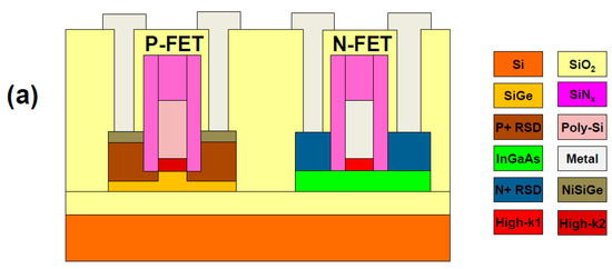
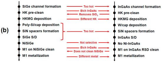
Figure 21.
(a) Schematic of devices cross section and (b) process flow of 2D hybrid InGaAs/SiGe CMOS technology with representative best-known process for n- and p-MOSFET. Non-compatible process steps are highlighted in red in the process flow description.
The main problem with integration of III-V on Si is the difficulty of direct growth of these materials with high epitaxial quality on Si. There are many methods to achieve this goal e.g., lateral growth, wafer bonding and using advanced GeSnSi buffer layers prior to III-V growth. The best way to manufacture 3D transistors is to grow III/V material in a trench when the Si of a Si-fin is etched and refilled by the III-V material for 3D transistor structures.
The full process flow for an InGaAs FinFET is demonstrated in Figure 22. The lowest defect density of 8 × 108 cm−2 was obtained on “V” shaped bottom trenches, where GaAs nucleation occurs only on {111} Si planes, minimizing the interfacial energy and preventing the formation of anti-phase boundaries. InAs and GaSb are thought to be promising candidates to replace Si in sub-7 nm CMOS devices due to their respective high electron and hole mobility [149].
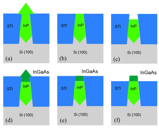
Figure 22.
Summary of process flow of formation fin when (a) post InP deposited; (b) InP chemical mechanical polish (CMP); (c) InP recess; (d) InGaAs growth; (e) InGaAs CMP; (f) STI oxide recess. Reprinted with permission from [151]. Copyright Solid State Electron, 2016.
The deposition of III-V material was done by metal organic chemical vapor deposition (MOCVD) on large CMOS compatible on-axis Si (001) substrates, using a thin buffer layer stack to manage thermal mismatch. The growth rate on the different planes is manipulated by the chosen metal organic vapor phase epitaxy (MOVPE) growth conditions. Parameters such as the growth temperature, reactor pressure, partial pressure of the precursors, V/III ratio, pattern mask ratio as well as the effective SAG rate have a strong impact on the surface reconstruction and on all kinetic processes (ad- and desorption of precursors, decomposition, diffusion, incorporation etc.). The interplay of above parameters defines the final growth rate hierarchy and hence the ridge formation [150].
The replacement of Si fins has proven to be a very versatile technique, allowing for the fabrication of FinFET, GAA and dual nanowire devices from the same basic flow. This process has enabled the first demonstration of fully integrated III-V devices on 300 mm Si substrates in a very large scale integration (VLSI) compatible flow. For the FinFET architecture, the unintentional background doping from the carbon inherent in the metal organic precursors requires development of a p-type doping solution to suppress S/D leakage through the InP buffer layer. Mg doping was found to be effective to p-type dope the InP grown on patterned substrates and consequently reduce the S/D leakage path. However, introducing Mg to the heterostructure results in a significant decrease in mobility due to increased coulombic scattering. By addressing the issue of the p-type doping degrading performance, the InP buffer was removed to create GAA devices.
The GAA architecture has also the advantage of increased electrostatics over that of the FinFET. The GAA transistors showed significant improvement in peak gm (1030 lS/lm vs. 588 lS/lm) as well as in subthreshold swing when Vds = Vdd (SSSAT:125 mV/dec vs. 178 mV/dec) compared to the FinFETs. The thermal budget for the gate stack was found to have a large impact on device performance. A comparison of high-k first to high-k last processing using the FinFET showed that the high-k/III-V interface degrades when exposed to >500 °C processing. This results also a significant decrease in the peak gm and increase in SSSAT.
A dual nanowire structure with a diameter as small as 6 nm was successfully demonstrated in a modified version of the GAA flow. The nanowire devices show excellent SSSAT values as low as 66 mV/dec despite having the same gate stack as the larger GAA devices. While many challenges still remain for 300 mm wafer based III-V devices to achieve the potential lattice matched substrates, these results are significant step towards the ultimate realization of III-V VLSI technology [151]. The TEM cross sectional images of different fabricated device structures using the dummy fin removed process are showed in Figure 23.
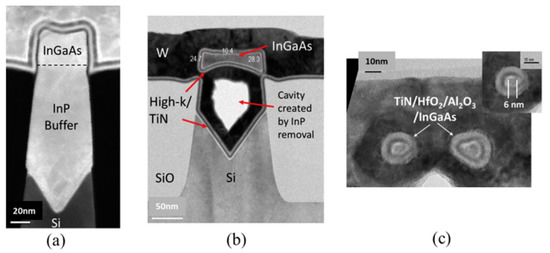
Figure 23.
TEM cross sectional images of different device structures fabricated using the dummy fin removed process as (a) FinFET, (b) Gate-all-around (GAA) and (c) dual-channel nanowires. Reprinted with permission from [151]. Copyright Solid State Electron, 2016.
7. Challenges in Circuit Design
In order to continue the “Moore’s law”, the circuit designs are becoming more and more important. When the critical dimensions (CD) of the IC move to almost atomic size, the simple down scaling cannot be further continued. In circuit design, many issues e.g., leakage increase, gain decrease, and the sensitivity and tolerance of process in the manufacturing need to be pre-consider and calculated. Although many technical challenges may come forward and it is difficult to achieve the CD limit (3 nm), but the circuit designs are still able to evolve novel solutions to address many of these challenges.
8. Conclusions
This article has highlighted and compared the process of planar (2D) and 3D FETs. An overall view over the process flow of 2D and 3D FETs shows many similarities steps except the formation of fins cause new challenges in the fabrication. These challenges are addressed to the issues e.g., gate and spacer patterning, forming uniform fins and the growth of SiGe stressor material on source/drain regions.
At first, a state-of-art lithography to form the nano-scale patterns is required. Nowadays, 193 nm ArF immersion with self-aligned double patterning and self-aligned quadruple patterning techniques are used for lithography of 22 nm node and beyond.
Extreme ultraviolet lithography is a promising technique as well, but the high cost of this technique requires a second thought for implementing it for mass production.
In planar transistors, SiO2 layer as gate oxide was abandoned already in 45 nm technology node and HfO2 was introduced instead due to its high dielectric constant and a relatively large bandgap. However, one of the main challenges of HfO2 integration in nano transistors is the thermal instability of HfO2/Si contact. There is usually a SiOx interlayer between HfO2 and Si substrate. The thickness of SiOx interlayer as well as the high-k dielectric have been constantly decreased leading to a decrease of the equivalent oxide thickness of gate dielectric.
The traditional Si polycrystalline as gate material was also replaced with a metal gate e.g., TiAlN and TiN in a gate-last approach to avoid crystallizaitons of the high-k dielectric during the thermal treatment for dopants activation.
To have a full control to form a Si fin with defined dimensions is a difficult task. It is especially critical to define the fin’s height by etching the shallow trench isolation oxide. The variation in fin height influences electrical properties of transistors, e.g., the threshold voltage. This indicates (dry or wet) etching step needs more attention to be paid for 3D transistors compared to the planar ones.
Dopant implantation of the fins requires a profile with conformal distribution otherwise the drive current of the transistors is degraded. To implant the fins in an array is a difficult task due to the shadowing caused by the neighboring fins. An alternative technique is using plasma doping with optimized process parameters.
SiGe layers are grown selectively in source/drain areas to create strain in the channel region. The selective epitaxy in the planar transistor is performed in the recessed areas while for 3D FETs is intended to elevate in the source/drain. The epi-layers on 3D FETs may involve in several problems e.g., strain relaxation on the fins’ faceted shape leading to higher defect density and pattern dependency effect due to different transistor architecture and their density in the chip.
In final, most of the presented process challenges in this article are undergoing developments or have partially solved. However, the most critical issue of future downscaling of transistors is the dramatic increase of manufacturing cost due to the use of innovative techniques e.g., EUVL. One way to reach a solution is the increase of wafer diameter from present 300 mm to 450 mm. However, there is a big skepticism to use such big wafers due to their heavy weight totally new mechanical robot systems have to be developed. Furthermore, the process time will remarkably increase in terms of low rate of warming and cooling of such big wafers.
There is a better solution to overcome these difficulties by using 3D structures instead of continuously downscaling the transistors. This effort would extend our research for many years in future to integrate many layers or devices vertically in the chip.
Acknowledgments
This work was supported by the National Key Research and Development Program of China under Grant No. 2016YFA0301701, and the Youth Innovation Promotion Association of the Chinese Academy of Sciences under Grant No. 2016112.
Conflicts of Interest
The authors declare no conflicts of interest.
References
- Colinge, J.P. (Ed.) The SOI MOSFET: From Single Gate to Multigate. In FinFETs and Other Multi-Gate Transistors; Tyndall National Institute: Cork, Ireland, 2008; pp. 2–4. [Google Scholar]
- Soitec Official Website. Available online: https://www.soitec.com/en (accessed on 21 June 2017).
- Veloso, A.; Ragnarsson, L.Å.; Cho, M.J.; Devriendt, K.; Kellens, K.; Sebaai, F.; Suhard, S.; Brus, S.; Crabbe, Y.; Schram, T. Gate-last vs. gate-first technology for aggressively scaled EOT logic/RF CMOS. In Proceedings of the IEEE 2011 Symposium on VLSI Technology (VLSIT), Honolulu, HI, USA, 14–16 June 2011; pp. 34–35. [Google Scholar]
- Mertens, H.; Ritzenthaler, R.; Hikavyy, A.; Kim, M.S.; Tao, Z.; Wostyn, K.; Chew, S.A.; de Keersgieter, A.; Mannaert, G.; Rosseel, E.; et al. Gate-All-Around MOSFETs based on Vertically Stacked Horizontal Si Nanowires in a Replacement Metal Gate Process on Bulk Si Substrates. In Proceedings of the 2016 IEEE Symposium on VLSI Technology, Honolulu, HI, USA, 14–16 June 2016. [Google Scholar] [CrossRef]
- Leading at the Edge, Technology and Manufacturing Day (Intel). Available online: https://www.intc.com/default.aspx?SectionId=817fbab8-2828-44a2-91a0-f10cb8ac2b03&LanguageId=1&EventId=637d959b-e595–4f0e-843e-5ee9af9d6520 (accessed on 20 June 2017).
- IBM Research Alliance Builds New Transistor for 5 nm Technology (IBM). Available online: https://www-03.ibm.com/press/us/en/pressrelease/52531.wss (accessed on 20 June 2017).
- Kuhn, K.J. Considerations for Ultimate CMOS Scaling. IEEE Trans. Electron Devices 2012, 59, 1813–1828. [Google Scholar] [CrossRef]
- Pikus, F.G.; Torres, A. Advanced multi-patterning and hybrid lithography techniques. In Proceedings of the 2016 21st Asia and South Pacific Design Automation Conference (ASP-DAC), Macau, China, 25–28 January 2016. [Google Scholar] [CrossRef]
- Yaegashi, H. Pattern Fidelity control in Multi-patterning towards 7 nm node. In Proceedings of the 2016 IEEE 16th International Conference on Nanotechnology (IEEE-NANO), Sendai, Japan, 22–25 August 2016. [Google Scholar] [CrossRef]
- Jiang, J.; Chakrabarty, S.; Yu, M.; Ober, C.K. Metal oxide nanoparticle photoresists for EUV patterning. J. Photopolym. Sci. Technol. 2014, 27, 663–666. [Google Scholar] [CrossRef]
- Mulkens, J.; Hanna, M. Overlay and Edge Placement Control Strategies for the 7-nm node using EUV and ArF lithography. In Extreme Ultraviolet (EUV) Lithography VI; SPIE: San Jose, CA, USA, 2016; Volume 9422. [Google Scholar] [CrossRef]
- Wu, Q. Key points in 14 nm photolithographic process development, challenges and process window capability. In Proceedings of the 2017 China Semiconductor Technology International Conference (CSTIC), Shanghai, China, 12–13 March 2017. [Google Scholar] [CrossRef]
- Verstappen, L.; Mos, E. Holistic overlay control for multi patterning process layers at the 10 nm and 7 nm nodes. In Metrology, Inspection, and Process Control for Microlithography XXX; SPIE: San Jose, CA, USA, 2016; Volume 9778. [Google Scholar] [CrossRef]
- Pirati, A.; Peeters, R. EUV lithography performance for manufacturing: Status and outlook. In Extreme Ultraviolet (EUV) Lithography VII; SPIE: San Jose, CA, USA, 2016; Volume 9776. [Google Scholar] [CrossRef]
- Pirati, A.; Peeters, R. Performance overview and outlook of EUV lithography systems. In Extreme Ultraviolet (EUV) Lithography VI; SPIE: San Jose, CA, USA, 2016; Volume 9422. [Google Scholar] [CrossRef]
- Simone, D.D.; Mao, M. Metal Containing Resist Readiness for HVM EUV Lithography. J. Photopolym. Sci. Technol. 2016, 29, 501–507. [Google Scholar] [CrossRef]
- Mamezaki, D.; Watanabe, M. Development of the Transmittance Measurement for EUV Resist by Direct Resist Coating on a Photodiode. J. Photopolym. Sci. Technol. 2016, 29, 749–752. [Google Scholar] [CrossRef]
- Yoda, Y.; Hayakawa, A. Next-generation immersion scanner optimizing on-product performance for 7 nm node. In Optical Microlithography XXIX; SPIE: San Jose, CA, USA, 2016; Volume 9780. [Google Scholar] [CrossRef]
- Wojdyla, A.; Donoghue, A. Aerial imaging study of the mask-induced line-width roughness of EUV lithography masks. In Extreme Ultraviolet (EUV) Lithography VII; SPIE: San Jose, CA, USA, 2015; Volume 9776. [Google Scholar] [CrossRef]
- Antohe, A.O.; Balachandran, D. SEMATECH produces defect-free EUV mask blanks: Defect yield and immediate challenges. In Extreme Ultraviolet (EUV) Lithography VI; SPIE: San Jose, CA, USA, 2015; Volume 94221B. [Google Scholar] [CrossRef]
- Jan, C.-H.; Bhattacharya, U.; Brain, R.; Choi, S.-J.; Curello, G.; Gupta, G.; Hafez, W.; Jang, M.; Kang, M.; Komeyli, K.; et al. A 22 nm SoC Platform Technology Featuring 3-D Tri-Gate and High-k/Metal Gate, Optimized for Ultra Low Power, High Performance and High Density SoC Applications. In Proceedings of the 2012 IEEE International Electron Devices Meeting (IEDM), San Francisco, CA, USA, 10–13 December 2012; pp. 44–47. [Google Scholar]
- Jan, C.-H.; Agostinelli, M.; Buehler, M.; Chen, Z.-P.; Choi, S.-J.; Curello, G.; Deshpande, H.; Gannavaram, S.; Hafez, W.; Jalan, U.; et al. A 32 nm SoC Platform Technology with 2nd Generation High-k/Metal Gate Transistors Optimized for Ultra Low Power, High Performance, and High Density Product Applications. In Proceedings of the 2009 IEEE International Electron Devices Meeting (IEDM), Baltimore, MD, USA, 7–9 December 2009; pp. 647–650. [Google Scholar]
- Conley, A. FinFET vs. FD-SOI Key Advantages & Disadvantages. ChipEx 2014, 30 April 2014. [Google Scholar]
- Kuhn, K.J.; Murthy, A.; Kotlyar, R.; Kuhn, M. Past, Present and Future: SiGe and CMOS Transistor Scaling. ECS Trans. 2010, 33, 3–17. [Google Scholar]
- Kise, N.; Kinoshita, H.; Yukimachi, A.; Kanazawa, T.; Miyamoto, Y. Fin width dependence on gate controllability of InGaAs channel FinFETs with regrown source/drain. Solid-State Electron. 2016, 126, 92–95. [Google Scholar] [CrossRef]
- Jan, C.-H.; Al-Amoody, F.; Chang, H.-Y.; Chang, T.; Chen, Y.-W.; Dias, N.; Hafez, W.; Ingerly, D.; Jang, M.; Karl, E.; et al. A 14 nm SoC Platform Technology Featuring 2nd Generation Tri-Gate Transistors, 70 nm Gate Pitch, 52 nm Metal Pitch, and 0.0499 μm2 SRAM cells, Optimized for Low Power, High Performance and High Density SoC Products. In Proceedings of the 2015 Symposium on VLSI Technology (VLSI Technology), Kyoto, Japan, 16–18 June 2015; pp. T12–T13. [Google Scholar]
- Jacob, A.P.; Xie, R.; Sung, M.G.; Liebmann, L.; Lee, R.T.P.; Taylor, B. Scaling Challenges for Advanced CMOS Devices. Int. J. High Speed Electron. Syst. 2017, 26, 2–76. [Google Scholar] [CrossRef]
- Matsukawa, T.; Liu, Y.; Endo, K.; Ouchi, S.-I.; Masahara, M. Variability origins of FinFETs and perspective beyond 20 nm node. In Proceedings of the 2011 IEEE International SOI Conference (SOI), Tempe, AZ, USA, 3–6 October 2011. [Google Scholar] [CrossRef]
- Kavalieros, J.; Doyle, B.; Datta, S.; Dewey, G.; Doczy, M.; Jin, B.; Lionberger, D.; Metz, M.; Rachmady, W.; Radosavljevic, M. Tri-gate Transistor Architecture with High-k Gate Dielectrics, Metal Gates and Strain Engineering. In Proceedings of the 2006 Symposium on VLSI Technology, Digest of Technical Papers, Honolulu, HI, USA, 13–15 June 2006. [Google Scholar] [CrossRef]
- Kuhn, K.J. CMOS Transistor Scaling Past 32 nm and Implications on Variation. In Proceedings of the 2010 IEEE/SEMI Advanced Semiconductor Manufacturing Conference (ASMC), San Francisco, CA, USA, 11–13 July 2010. [Google Scholar] [CrossRef]
- Veloso, A.; De Keersgieter, A.; Matagne, P.; Horiguchi, N.; Collaert, N. Advances on doping strategies for triple-gate finFETs and lateral gate-all-around nanowire FETs and their impact on device performance. Mater. Sci. Semicond. Proc. 2017, 62, 2–12. [Google Scholar] [CrossRef]
- Current, M.I. Ion implantation of advanced silicon devices: Past, present and future. Mater. Sci. Semicond. Proc. 2017, 62, 13–22. [Google Scholar] [CrossRef]
- Ang, K.-W.; Barnett, J.; Loh, W.-Y.; Huang, J.; Min, B.-G.; Hung, P.Y.; Ok, I.; Yum, J.H.; Bersuker, G.; Rodgers, M.; et al. 300 mm FinFET results utilizing conformal, damage free, ultra shallow junctions (Xj∼5 nm) formed with molecular monolayer doping technique. In Proceedings of the 2011 IEEE International Electron Devices Meeting (IEDM), Washington, DC, USA, 5–7 December 2011; Volume 1–35, p. 35. [Google Scholar]
- Pidin, S.; Mori, T.; Inoue, K.; Fukuta, S.; Itoh, N.; Mutoh, E.; Ohkoshi, K.; Nakamura, R.; Kobayashi, K.; Kawamura, K.; et al. A novel strain enhanced CMOS architecture using selectively deposited high tensile and high compressive silicon nitride films. In Proceedings of the IEEE International Electron Devices Meeting, IEDM Technical Digest, San Francisco, CA, USA, 13–15 December 2004; pp. 213N–216N. [Google Scholar]
- Xu, N.; Ho, B.; Choi, M.; Moroz, V.; Liu, T.J.K. Effectiveness of stressors in aggressively scaled FinFETs. IEEE Trans. Electron Devices 2012, 59, 1592–1598. [Google Scholar] [CrossRef]
- Ghani, T.; Armstrong, M.; Auth, C.; Bost, M.; Charvat, P.; Glass, G.; Hoffmann, T.; Johnson, K.; Kenyon, C.; Klaus, J.; et al. A 90 nm high volume manufacturing logic technology featuring novel 45 nm gate length strained silicon CMOS transistors. In Proceedings of the IEEE International Electron Devices Meeting, IEDM ′03 Technical Digest, Washington, DC, USA, 8–10 December 2003. [Google Scholar]
- Auth, C.; Allen, C.; Blattner, A.; Bergstrom, D.; Brazier, M.; Bost, M.; Buehler, M.; Chikarmane, V.; Ghani, T.; Glassman, T. A 22 nm high performance and low-power CMOS technology featuring fully-depleted tri-gate transistors, self-aligned contacts and high density MIM capacitors. In Proceedings of the 2012 IEEE Symposium on VLSI Technology, Honolulu, HI, USA, 12–14 June 2012; pp. 131–132. [Google Scholar]
- Thompson, S.; Sun, G.; Wu, K.; Lim, J.; Nishida, T. Key differences for process-induced uniaxial vs. substrate-induced biaxial stressed Si and Ge channel MOSFETs. In Proceedings of the IEEE International Electron Devices Meeting, IEDM Technical Digest, San Francisco, CA, USA, 13–15 December 2004; pp. 221–224. [Google Scholar]
- Mistry, K.; Allen, C.; Auth, C.; Beattie, B.; Bergstrom, D.; Bost, M.; Brazier, M.; Buehler, M.; Cappellani, A.; Chau, R.; et al. A 45 nm logic technology with high-k+ metal gate transistors, strained silicon, 9 Cu interconnect layers, 193 nm dry patterning, and 100% Pb-free packaging. In Proceedings of the IEEE International Electron Devices Meeting (IEDM), Washington, DC, USA, 10–12 December 2007; pp. 247–250. [Google Scholar]
- Bohr, M.; Mistry, K. Intel’s Revolutionary 22 nm Transistor Technology. 2011. Available online: http://download.intel.com/newsroom/kits/22nm/pdfs/22nm-Details_Presentation.pdf (accessed on 2 October 2017).
- Ohta, H.; Kim, Y.; Shimamune, Y.; Sakuma, T.; Hatada, A.; Katakami, A.; Soeda, T.; Kawamura, K.; Kokura, H.; Morioka, H.; et al. High performance 30 nm gate bulk CMOS for 45 nm node with/spl Sigma/-shaped SiGe-SD. In Proceedings of the IEEE International Electron Devices Meeting, IEDM Technical Digest, Washington, DC, USA, 5 December 2005; pp. 247–250. [Google Scholar]
- Tamura, N.; Shimamune, Y. 45 nm CMOS technology with low temperature selective epitaxy of SiGe. Appl. Surf. Sci. 2008, 254, 6067–6071. [Google Scholar] [CrossRef]
- Qin, C.; Yin, H.; Wang, G.; Hong, P.; Ma, X.; Cui, H.; Lu, Y.; Meng, L.; Yin, H.; Zhong, H.; et al. Study of sigma-shaped source/drain recesses for embedded-SiGe pMOSFETs. Microelectron. Eng. 2017, 181, 22–28. [Google Scholar] [CrossRef]
- Xiao, H. 3D IC Devices. In Technologies, and Manufacturing; Society of Photo-Optical Instrumentation Engineers (SPIE): Bellingham, WA, USA, 2016. [Google Scholar]
- Dutartre, D.; Talbot, A.; Loubet, N. Facet propagation in Si and SiGe epitaxy or etching. ECS Trans. 2006, 3, 473–487. [Google Scholar]
- Mujumdar, S.; Maitra, K.; Datta, S. Layout-dependent strain optimization for p-channel trigate transistors. IEEE Trans. Electron Devices 2012, 59, 72–78. [Google Scholar] [CrossRef]
- Hållstedt, J.; Kolahdouz, M.; Ghandi, R.; Radamson, H.H.; Wise, R. Pattern dependency in selective epitaxy of B-doped SiGe layers for advanced metal oxide semiconductor field effect transistors. J. Appl. Phys. 2008, 103, 054907. [Google Scholar] [CrossRef]
- Kolahdouz, M.; Hållstedt, J.; Khatibi, A.; Östling, M.; Wise, R.; Riley, D.J.; Radamson, H.H. Comprehensive evaluation and study of pattern dependency behavior in selective epitaxial growth of B-doped SiGe layers. IEEE Trans. Nanotechnol. 2009, 8, 291–297. [Google Scholar] [CrossRef]
- Wang, G.; Moeen, M.; Abedin, A.; Xu, Y.; Luo, J.; Guo, Y.; Qin, C.; Tang, Z.; Yin, H.; Li, J.; et al. Impact of pattern dependency of SiGe layers grown selectively in source/drain on the performance of 22 nm node pMOSFETs. Solid-State Electron. 2015, 114, 43–48. [Google Scholar] [CrossRef]
- Qin, C.; Wang, G.; Kolahdouz, M.; Luo, J.; Yin, H.; Yang, P.; Radamson, H.H. Impact of pattern dependency of SiGe layers grown selectively in source/drain on the performance of 14 nm node FinFETs. Solid-State Electron. 2016, 124, 10–15. [Google Scholar] [CrossRef]
- Radamson, H.; Thylen, L. Monolithic Nanoscale Photonics-Electronics Integration in Silicon and Other Group IV Elements; Elsevier: San Diego, CA, USA, 2014. [Google Scholar]
- Wang, G.; Luo, J.; Liu, J.; Yang, T.; Xu, Y.; Li, J.; Yin, H.; Yan, J.; Zhu, H.; Zhao, C.; et al. pMOSFETs Featuring ALD W Filling Metal Using SiH4 and B2H6 Precursors in 22 nm Node CMOS Technology. Nanoscale Res. Lett. 2017, 12, 306. [Google Scholar] [CrossRef] [PubMed]
- Hansson, G.V.; Radamsson, H.H.; Ni, W.X. Strain and relaxation in Si-MBE structures studied by reciprocal space mapping using high resolution X-ray diffraction. J. Mater. Sci. Mater. Electron. 1995, 6, 292–297. [Google Scholar] [CrossRef]
- Wang, G.L.; Moeen, M.; Abedin, A.; Kolahdouz, M.; Luo, J.; Qin, C.L.; Zhu, H.L.; Yan, J.; Yin, H.; Li, J.; et al. Optimization of SiGe selective epitaxy for source/drain engineering in 22 nm node complementary metal-oxide semiconductor (CMOS). J. Appl. Phys. 2013, 114, 123511. [Google Scholar] [CrossRef]
- Radamson, H.H.; Joelsson, K.B.; Ni, W.-X.; Hultman, L.; Hansson, G.V. Characterization of highly boron-doped Si, Si1−xGex and Ge layers by high-resolution transmission electron microscopy. J. Cryst. Growth 1995, 157, 80–84. [Google Scholar] [CrossRef]
- Nur, O.; Willander, M.; Hultman, L.; Radamson, H.H.; Hansson, G.V. CoSi2/Si1−xGex/Si(001) heterostructures formed through different reaction routes: Silicidation-induced strain relaxation, defect formation, and interlayer diffusion. J. Appl. Phys. 1995, 78, 7063–7069. [Google Scholar] [CrossRef]
- Hallstedt, J.; Blomqvist, M.; Persson, P.O.A.; Hultman, L.; Radamson, H.H. The effect of carbon and germanium on phase transformation of nickel on Si1−x−yGexCy epitaxial layers. J. Appl. Phys. 2004, 95, 2397. [Google Scholar] [CrossRef]
- Takeuchi, H.; King, T.-J. Scaling limits of hafnium—Silicate films for gate-dielectric applications. Appl. Phys. Lett. 2003, 83, 788–790. [Google Scholar] [CrossRef]
- Seong, N.J.; Yoon, S.G.; Yeom, S.J.; Woo, H.K.; Kil, D.S.; Roh, J.S.; Sohn, H.C. Effect of nitrogen incorporation on improvement of leakage properties in high-k HfO2 capacitors treated by N2-plasma. Appl. Phys. Lett. 2005, 87, 132903. [Google Scholar] [CrossRef]
- Zhao, C.; Witters, T.; Brijs, B.; Bender, H.; Richard, O.; Caymax, M.; Heeg, T.; Schubert, J.; Afanas’ev, V.V.; Stesmans, A.; Schlom, D.G. Ternary rare-earth metal oxide high-k layers on silicon oxide. Appl. Phys. Lett. 2005, 86, 132903. [Google Scholar] [CrossRef]
- Barlage, D.; Arghavani, R.; Dewey, G.; Doczy, M.; Doyle, B.; Kavalieros, J.; Murthy, A.; Roberds, B.; Stokley, P.; Chau, R. High-frequency response of 100 nm integrated CMOS transistors with high-k gate dielectrics. In Proceedings of the IEEE International Electron Devices Meeting, Washington, DC, USA, 2–5 December 2001. [Google Scholar]
- Robertson, J. Band offsets of wide-band-gap oxides and implications for future electronic devices. J. Vac. Sci. Technol. B Microelectron. Nanom. Struct. Proc. Meas. Phenom. 2000, 18, 1785–1791. [Google Scholar] [CrossRef]
- Brar, B.; Wilk, G.D.; Seabaugh, A.C. Direct extraction of the electron tunneling effective mass in ultrathin SiO2. Appl. Phys. Lett. 1996, 69, 2728–2730. [Google Scholar] [CrossRef]
- Vogel, E.M.; Ahmed, K.Z.; Hornung, B.; Henson, W.K.; McLarty, P.K.; Lucovsky, G.; Hauser, J.R.; Wortman, J.J. Modeled tunnel currents for high dielectric constant dielectrics. IEEE Trans. Electron Devices 1998, 45, 1350–1355. [Google Scholar] [CrossRef]
- Johansson, M.; Yousif, M.Y.A.; Lundgren, P.; Bengtsson, S.; Sundqvist, J.; Hårsta, A.; Radamson, H.H. HfO2 gate dielectrics on strained-Si and strained-SiGe layers. Semicond. Sci. Technol. 2003, 18, 820. [Google Scholar] [CrossRef]
- Choi, J.H.; Mao, Y.; Chang, J.P. Development of hafnium based high-k materials—A review. Mater. Sci. Eng. R Rep. 2011, 72, 97–136. [Google Scholar] [CrossRef]
- Zheng, Y.B.; Wang, S.J.; Huan, C.H.A. Microstructure-dependent band structure of HfO2 thin films. Thin Solid Films 2006, 504, 197–200. [Google Scholar] [CrossRef]
- Hwang, W.S.; Shen, C.; Wang, X.; Chan, D.S.H.; Cho, B.J. A Novel Hafnium Carbide HfCx Metal Gate Electrode for NMOS Device Application. In Proceedings of the IEEE Symposium on VLSI Technology, Kyoto, Japan, 12–14 June 2007; pp. 156–157. [Google Scholar]
- Wilk, G.D.; Wallace, R.M.; Anthony, J.M. High-k gate dielectrics: Current status and materials properties considerations. J. Appl. Phys. 2001, 89, 5243–5275. [Google Scholar] [CrossRef]
- Robertson, J. High dielectric constant gate oxides for metal oxide Si transistors. Rep. Prog. Phys. 2006, 69, 327–396. [Google Scholar] [CrossRef]
- Xiong, K.; Peacock, P.W.; Robertson, J. Fermi level pinning and Hf–Si bonds at HfO2: Polycrystalline silicon gate electrode interfaces. Appl. Phys. Lett. 2005, 86, 012904. [Google Scholar] [CrossRef]
- Hobbs, C.C.; Fonseca, L.R.C.; Knizhnik, A.; Dhandapani, V.; Samavedam, S.B.; Taylor, W.J.; Grant, J.M.; Dip, L.G.; Triyoso, D.H.; Hegde, R.I.; et al. Fermi-level pinning at the polysilicon/metal oxide interface-Part I. IEEE Trans. Electron Devices 2004, 51, 971–977. [Google Scholar] [CrossRef]
- George, S.M. Atomic Layer Deposition: An Overview. Chem. Rev. 2010, 110, 111–131. [Google Scholar] [CrossRef] [PubMed]
- Puurunen, R.L. Surface chemistry of atomic layer deposition: A case study for the trimethylaluminum/water process. J. Appl. Phys. 2005, 97, 121301. [Google Scholar] [CrossRef]
- Heo, S.C.; Choi, C. Plasma atomic layer deposited TiN metal gate for three dimensional device applications: Deposition temperature, capping metal and post annealing. Microelectron. Eng. 2012, 94, 11–13. [Google Scholar] [CrossRef]
- Jeon, S.; Park, S. Fabrication of Robust Triple- Ti1−xAlxN Metal Gate by Atomic Layer Deposition. J. Electrochem. Soc. 2010, 157, H1101–H1105. [Google Scholar] [CrossRef]
- Lee, A.; Fuchigami, N.; Pisharoty, D.; Hong, Z.; Haywood, E.; Joshi, A.; Mujumdar, S.; Bodke, A.; Karlsson, O.; Kim, H.; et al. Atomic layer deposition of HfxAlyCz as a work function material in metal gate MOS devices. J. Vac. Sci. Technol. A 2014, 32, 01A118. [Google Scholar] [CrossRef]
- Dekkers, H.F.W.; Lima, L.P.B.; Van Elshocht, S. Conductivity Improvements of Atomic Layer Deposited Ta3N5. ECS Trans. 2013, 58, 195–202. [Google Scholar] [CrossRef]
- Ragnarsson, L.A.; Chew, S.A.; Dekkers, H.; Luque, M.T.; Parvais, B.; De Keersgieter, A.; Devriendt, K.; Van Ammel, A.; Schram, T.; Yoshida, N.; et al. Highly scalable bulk FinFET Devices with Multi-VT options by conductive metal gate stack tuning for the 10-nm node and beyond. In Proceedings of the 2014 Symposium on VLSI Technology (VLSI-Technology): Digest of Technical Papers, Honolulu, HI, USA, 9–12 June 2014; pp. 1–2. [Google Scholar]
- Cho, G.H.; Rhee, S.W. Plasma-Enhanced Atomic Layer Deposition of TaCxNy Films with tert-Butylimido Tris-diethylamido Tantalum and Methane/Hydrogen Gas. Electrochem. Solid-State Lett. 2010, 13, H426–H427. [Google Scholar] [CrossRef]
- Triyoso, D.H.; Gregory, R.; Schaeffer, J.K.; Werho, D.; Li, D.; Marcus, S.; Wilk, G.D. Atomic layer deposited TaCy metal gates: Impact on microstructure, electrical properties, and work function on HfO2 high-k dielectrics. J. Appl. Phys. 2007, 102, 104509. [Google Scholar] [CrossRef]
- Xiang, J.; Zhang, Y.; Li, T.; Wang, X.; Gao, J.; Yin, H.; Li, J.; Wang, W.; Ding, Y.; Xu, C.; et al. Investigation of thermal atomic layer deposited TiAlX (X = N or C) film as metal gate. Solid-State Electron. 2016, 122, 64–69. [Google Scholar] [CrossRef]
- Xiang, J.; Li, T.; Zhang, Y.; Wang, X.; Gao, J.; Cui, H.; Yin, H.; Li, J.; Wang, W.; Ding, Y.; et al. Investigation of TiAlC by Atomic Layer Deposition as N Type Work Function Metal for FinFET. ECS J. Solid State Sci. Technol. 2015, 4, 441–444. [Google Scholar] [CrossRef]
- Xiang, J.; Ding, Y.; Du, L.; Xu, C.; Li, T.; Wang, X.; Li, J.; Zhao, C. Investigation of N Type Metal TiAlC by Thermal Atomic Layer Deposition Using TiCl4 and TEA as Precursors. ECS J. Solid State Sci. Technol. 2016, 5, 299–303. [Google Scholar] [CrossRef]
- Xiang, J.; Li, T.; Wang, X.; Du, L.; Ding, Y.; Wang, W.; Li, J.; Zhao, C. Thermal Atomic Layer Deposition of TaAlC with TaCl5 and TMA as Precursors. ECS J. Solid State Sci. Technol. 2016, 5, 633–636. [Google Scholar] [CrossRef]
- Xiang, J.; Wang, X.; Li, T.; Gao, J.; Han, K.; Yu, J.; Wang, W.; Li, J.; Zhao, C. Investigation of Thermal Atomic Layer Deposited TaAlC with Low Effective Work-Function on HfO2 Dielectric Using TaCl5 and TEA as Precursors. ECS J. Solid State Sci. Technol. 2017, 6, 38–41. [Google Scholar] [CrossRef]
- Wang, G.; Xu, Q.; Yang, T.; Xiang, J.; Xu, J.; Gao, J.; Li, C.; Li, J.; Yan, J.; Chen, D.; et al. Application of atomic layer deposition tungsten (ALD W) as gate filling metal for 22 nm and beyond nodes CMOS technology. ECS J. Solid State Sci. Technol. 2014, 3, 82–85. [Google Scholar] [CrossRef]
- Xu, Q.; Luo, J.; Wang, G.; Yang, T.; Li, J.; Ye, T.; Chen, D.; Zhao, C. Application of ALD W films as gate filling metal in 22 nm HKMG-last integration: evaluation and improvement of the adhesion in CMP process. Microelectron. Eng. 2015, 137, 43–46. [Google Scholar] [CrossRef]
- Li, J.; Domenicucci, A.; Chidambarrao, D.; Greene, B.; Rovdedo, N.; Holt, J. Stress and strain measurements in semiconductor device channel areas by convergent beam electron diffraction. Mater. Res. Soc. Symp. Proc. 2006, 913. [Google Scholar] [CrossRef]
- Maszara, W.P.; Lin, M.R. FinFETs-Technology and circuit design challenges. In Proceedings of the 2013 ESSCIRC (ESSCIRC), Bucharest, Romania, 16–20 September 2013; pp. 3–8. [Google Scholar]
- Mérelle, T.; Curatola, G.; Nackaerts, A.; Collaert, N.; Van Dal, M.J.H.; Doornbos, G.; Doorn, T.S.; Christie, P.; Vellianitis, G.; Duriez, B.; et al. First observation of FinFET specific mismatch behavior and optimization guidelines for SRAM scaling. In Proceedings of the IEEE International Electron Devices Meeting (IEDM), San Francisco, CA, USA, 15–17 December 2008; pp. 241–244. [Google Scholar]
- Maeda, S.; Ko, Y.; Jeong, J.; Fukutome, H.; Kim, M.; Kim, S.; Choi, J.; Shin, D.; Oh, Y.; Lim, W.; et al. 3 Dimensional Scaling Extensibility on Epitaxial Source Drain Strain Technology toward Fin FET and Beyond. In Proceedings of the 2013 Symposium on VLSI Technology, Kyoto, Japan, 11–13 June 2013; pp. T88–T89. [Google Scholar]
- Huang, R.; Wang, R.; Zhuge, J.; Liu, C.; Yu, T.; Zhang, L.; Huang, X.; Ai, Y.; Zou, J.; Liu, Y.; et al. Characterization and analysis of gate-all-around Si nanowire transistors for extreme scaling. In Proceedings of the 2011 IEEE Custom Integrated Circuits Conference (CICC), San Jose, CA, USA, 19–21 September 2011; pp. 1–8. [Google Scholar]
- Lauer, I.; Loubeta, N.; Kimb, S.D.; Ott, J.A.; Mignot, S.; Venigalla, R.; Yamashita, T.; Standaert, T.; Faltermeier, J.; Basker, V.; et al. Si Nanowire CMOS Fabricated with Minimal Deviation from RMG FinFET Technology Showing Record Performance. In Proceedings of the 2015 Symposium on VLSI Technology Digest of Technical, Kyoto, Japan, 16–18 June 2015; pp. T140–T141. [Google Scholar]
- Bangsaruntip, S.; Balakrishnan, K.; Cheng, S.L.; Chang, J.; Brink, M.; Lauer, I.; Bruce, R.L.; Engelmann, S.U.; Pyzyna, A.; Cohen, G.M.; et al. Density scaling with gate-all-around silicon nanowire MOSFETs for the 10 nm node and beyond. In Proceedings of the 2013 IEEE International Electron Devices Meeting (IEDM), Washington, DC, USA, 9–11 December 2013. [Google Scholar]
- Yakimets, D.; Eneman, G.; Schuddinck, P.; Bao, T.H.; Bardon, M.G.; Raghavan, P.; Veloso, A.; Collaert, N.; Mercha, A.; Verkest, D.; et al. Vertical GAAFETs for the Ultimate CMOS Scaling. IEEE Trans. Electron Devices 2015, 62, 1433–1439. [Google Scholar] [CrossRef]
- Hergenrother, J.M.; Oh, S.-H.; Nigam, T.; Monroe, D.; Klemens, F.P.; Kornblit, A. The vertical replacement-gate (VRG) MOSFET. Solid-State Electron. 2002, 46, 939–950. [Google Scholar] [CrossRef]
- Basaran, C.; Lin, M. Damage mechanics of electromigration in microelectronics copper interconnects. Int. J. Mater. Struct. Integr. 2007, 1, 16–39. [Google Scholar] [CrossRef]
- Yau, L.D. Short Channel Effects: The Need for Junction Scaling. Solid-State Electron. 1974, 17, 1059–1063. [Google Scholar] [CrossRef]
- Jeong, U.; Zhao, U.; Guo, B.; Li, G.; Mehta, S. Requirements and Challenges in Ion Implanters for Sub-100 nm CMOS Device Fabrication, principles and practice of constraint programming. Appl. Accel. Res. Ind. 2003, 680, 697–700. [Google Scholar]
- Erokhin, Y.; Romig, T.; Kim, E.; Xu, J.; Guo, B.; Liu, J.; Shim, K.; Nunan, P. High Current Implant Precision Requirements for Sub-65 nm Logic Devices. In Proceedings of the AIP Conference, Marseille, France, 11–16 June 2006; Volume 866, pp. 520–523. [Google Scholar]
- Craig, M.; Sultan, A.; Banerjee, S.K. Carbon co-implantation for ultra-shallow P/sup +/−N junction formation. In Proceedings of the 11th International Conference on Ion Implantation Technology, Austin, TX, USA, 16–21 June 1996; pp. 665–667. [Google Scholar]
- Chiu, H.Y.; Fang, Y.K.; Juang, F.R. Effects of Carbon Co-Implantation on Transient Enhanced Diffusion and Performances of the Phosphorus Doped Ultra-Shallow Junction Nano NMOSFET. In Applied Mechanics and Materials; Trans Tech Publications: Zurich, Switzerland, 2013; pp. 98–102. [Google Scholar]
- Jacobson, D.C.; Bourdelle, K.; Gossmann, H.J.; Sosnowski, M.; Albano, M.A.; Babaram, V.; Poate, J.M.; Agarwal, A.; Perel, A.; Horsky, T. Decaborane, an alternative approach to ultra low energy ion implantation. In Proceedings of the Conference on Ion Implantation Technology, Alpbach, Austria, 17–22 September 2000; pp. 300–303. [Google Scholar]
- Renau, A. A better approach to molecular implantation. In Proceedings of the 2007 International Workshop on Junction Technology, Kyoto, Japan, 8–9 June 2007; pp. 107–112. [Google Scholar]
- Yang, C.L.; Li, C.I.; Lin, G.P.; Liu, R.; Hsu, B.C.; Chan, M.; Wu, J.; Colombeau, B.; Guo, B.; Gossmann, B.; et al. Benefits of cryo-implantation for 28 nm NMOS advanced junction formation. Semicond. Sci. Technol. 2012, 27, 045003. [Google Scholar] [CrossRef]
- Hu, C.; Xu, P.; Fu, C.; Zhu, Z.; Gao, X.; Jamshidi, A.; Noroozi, M.; Radamson, H. Characterization of Ni (Si, Ge) films on epitaxial SiGe (100) formed by microwave annealing. Appl. Phys. Lett. 2012, 101, 092101. [Google Scholar] [CrossRef]
- Liu, J.; Luo, J.; Simoen, E.; Niu, Y.X.; Yang, F.; Wang, G.; Wang, W.; Chen, D.; Li, J.; Zhao, C.; et al. Junction Control by Carbon and Phosphorus Co-Implantation in Pre-Amorphized Germanium. ECS J. Solid State Sci. Technol. 2016, 5, 315–319. [Google Scholar] [CrossRef]
- Foggiato, J.; Yoo, W.S. Millisecond flash annealing: Applications for USJ formation and optimization of device electrical characteristics. Mater. Sci. Eng. B 2005, 124, 219–222. [Google Scholar] [CrossRef]
- Paul, S.; Lerch, W. Implant Annealing: An Evolution from Soak over Spike to Millisecond Annealing. Mater. Sci. Forum 2008, 573–574, 207–228. [Google Scholar] [CrossRef]
- Xu, P.; Zhou, X.; Zhao, N.; Zhao, D.; Wu, D. Formation of ultra-shallow junctions with pre-amorphization implant and microwave annealing. In Proceedings of the 2013 13th International Workshop on Junction Technology (IWJT), Kyoto, Japan, 6–7 June 2013; pp. 91–93. [Google Scholar]
- Pawlak, B.J.; Duffy, R.; De Keersgieter, A. Doping Strategies for FinFETs. In Materials Science Forum; Trans Tech Publications: Zurich, Switzerland, 2008; Volume 573, pp. 333–338. [Google Scholar]
- Borland, J.O. Smartphones: Driving Technology to More than Moore 3-D Stacked Devices/Chips and More Moore FinFET 3-D Doping with High Mobility Channel Materials from 20/22 nm Production to 5/7 nm Exploratory Research. ECS Trans. 2015, 69, 11–20. [Google Scholar] [CrossRef]
- Vandervorst, W.; Eyben, P.; Jurzack, M.; Pawlak, B.; Duffye, R. Conformal doping of FINFETs: A fabrication and metrology challenge. In Proceedings of the International Symposium on VLSI Technology, Systems and Applications, Hsinchu, Taiwan, 21–23 April 2008; Volume 1066, pp. 449–456. [Google Scholar]
- Han, K.; Tang, S.; Rockwell, T.; Godet, L.; Persing, H.; Campbell, C.; Salimian, S. A novel plasma-based technique for conformal 3D FINFET doping. In Proceedings of the 2012 12th International Workshop on Junction Technology (IWJT), Shanghai, China, 14–15 May 2012; pp. 35–37. [Google Scholar]
- Izumida, T.; Okano, K.; Kanemura, T.; Kondo, M.; Inaba, S.; Itoh, S.I.; Aoki, N.; Toyoshima, Y. Advantage of Plasma Doping for Source/Drain Extension in Bulk Fin Field Effect Transistor. Jpn. J. Appl. Phys. 2011, 50, 04DC15. [Google Scholar] [CrossRef]
- Lenoble, D.; Anil, K.; De Keersgieter, A.; Eybens, P.; Collaert, N.; Rooyackers, R.; Brus, S.; Zimmerman, P.; Goodwin, M.; Vanhaeren, D.; et al. Enhanced performance of PMOS MUGFET via integration of conformal plasma-doped source/drain extensions. In Proceedings of the 2006 Symposium on VLSI Technology, Digest of Technical Papers, Honolulu, HI, USA, 13–15 June 2006; pp. 168–169. [Google Scholar]
- Duffy, R.; Shayesteh, M. FinFET doping; material science, metrology, and process modeling studies for optimized device performance. In Proceedings of the AIP Conference 18th International Conference on Ion Implantation Technology, Kyoto, Japan, 6–11 June 2010; Volume 1321, pp. 17–22. [Google Scholar]
- Colombeau, B.; Guo, B.; Gossmann, H.J.; Khaja, F.; Pradhan, N.; Waite, A.; Rao, K.V.; Thomidis, C.; Shim, K.; Henry, T.; et al. Advanced CMOS devices: Challenges and implant solutions. Phys. Status Solidi (a) 2014, 211, 101–108. [Google Scholar] [CrossRef]
- Wood, B.S.; Khaja, F.A.; Colombeau, B.P.; Sun, S.; Waite, A.; Jin, M.; Chen, H.; Chan, O.; Thanigaivelan, T.; Thanigaivelan, T.; et al. Fin doping by hot implant for 14 nm finfet technology and beyond. ECS Trans. 2013, 58, 249–256. [Google Scholar] [CrossRef]
- Huang, J.; Li, Q.; Chong, E. Challenges and solutions for 14 nm FinFET etching. In Proceedings of the IEEE 2015 China Semiconductor Technology International Conference (CSTIC), Shanghai, China, 15–16 March 2015. [Google Scholar]
- Barraud, S.; Lapras, V.; Samson, M.P. Vertically Stacked-NanoWires MOSFETs in a Replacement Metal Gate Process with Inner Spacer and SiGe Source/Drain. In Proceedings of the 2016 IEEE International Electron Devices Meeting (IEDM), San Francisco, CA, USA, 3–7 December 2016. [Google Scholar] [CrossRef]
- Banna, S.; Agarwal, A. Pulsed high-density plasmas for advanced dry etching processes. J. Vac. Sci. Technol. 2012, 30, 040801. [Google Scholar] [CrossRef]
- Kanarik, K.J.; Kamarthy, G.; Gottscho, R.A. Plasma etch challenges for FinFET transistors. Solid State Technol. 2012, 55, 15. [Google Scholar]
- Endo, K.; Noda, S.; Masahara, M. Fabrication of FinFETs by Damage-Free Neutral-Beam Etching Technology. IEEE Trans. Electron Devices 2006, 53, 1826–1832. [Google Scholar] [CrossRef]
- Brun, P.; Bailly, F.; Guillermet, M. Plasma etch challenges at 14 nm and beyond technology nodes in the BEOL. In Proceedings of the 2015 IEEE International Interconnect Technology Conference and 2015 IEEE Materials for Advanced Metallization Conference (IITC/MAM), Grenoble, France, 18–21 May 2015. [Google Scholar] [CrossRef]
- Schaepkens, M.; Standaert, T.E.F.M.; Rueger, N.R. Study of the SiO2-to-Si3N4 etch selectivity mechanism in inductively coupled fluorocarbon plasmas and a comparison with the SiO2-to-Si mechanism. Am. Vac. Soc. 1999, 17, 26–37. [Google Scholar] [CrossRef]
- Honda, M.; Katsunuma, T. Etch Challenges and Evolutions for Atomic-order Control. In Proceedings of the IEEE 16th International Conference on Nanotechnology (IEEE-NANO), Sendai, Japan, 22–25 August 2016. [Google Scholar]
- Xiong, W.W. Multigate MOSFET technology. In FinFETs and Other Multi-Gate Transistors; Colinge, J.-P., Ed.; Tyndall National Institute: Cork, Ireland, 2008; pp. 49–111. [Google Scholar]
- Redolfi, A.; Sleeckx, E.; Devriendt, K.; Shamiryan, D.; Vandeweyer, T.; Horiguchi, N.; Togo, M.; Wouter, J.M.D.; Jurczak, M.; Hoffmann, T.; et al. Bulk FinFET fabrication with new approaches for oxide topography control using dry removal techniques. Solid-State Electron. 2012, 71, 106–112. [Google Scholar] [CrossRef]
- Auth, C.; Cappellani, A.; Chun, J.-S.; Dalis, A.; Davis, A.; Ghani, T.; Glass, G.; Glassman, T.; Harper, M.; Hattendorf, M.; et al. 45 nm High-k + metal gate strain-enhanced transistors. In Proceedings of the IEEE Symposium on VLSI Technology, Honolulu, HI, USA, 17–19 June 2008. [Google Scholar]
- Sebaai, F.; Del Agua Borniquel, J.I.; Vos, R.; Absil, P.; Chiarella, T.; Vrancken, C.; Boelen, P.; Baiya, E. Poly-Silicon Etch with Diluted Ammonia: Application to Replacement Gate Integration Scheme. Solid State Phenom. 2009, 145, 207–210. [Google Scholar] [CrossRef]
- Sebaai, F.; Veloso, A.; Claes, M.; Devriendt, K.; Brus, S.; Absil, P.; Mertens, P.; De Gendt, S. Poly-Silicon Wet Removal for Replacement Gate Integration Scheme: Impact of Process Parameters on the Removal Rate. Solid State Phenom. 2012, 187, 53–56. [Google Scholar] [CrossRef]
- Takahashi, H.; Otsuji, M.; Snow, J.; Sebaai, F.; Arai, K.; Sato, M.; Nadahara, S. Wet Etching Behavior of Poly-Si in TMAH Solution. Solid State Phenom. 2012, 195, 42–45. [Google Scholar] [CrossRef]
- Hussain, M.M. Cleaning Challenges of High-k/Metal Gate Structure. In Handbook of Cleaning for Semiconductor Manufacturing—Fundamentals and Applications; Reinhardt, K.A., Reidy, R.F., Eds.; John Wiley & Sons, Inc.: Hoboken, NJ, USA, 2011; pp. 249–251. [Google Scholar] [CrossRef]
- Huff, H.R.; Richter, C.A.; Green, M.L.; Lucovsky, G.; Hattori, T. Ultrathin SiO2 and High-k Materials for ULSI Gate Dielectrics. In Proceedings of the Materials Research Society (MRS), Pittsburgh, PA, USA, 5–7 April 1999. [Google Scholar]
- Knotter, D.M. Etching Mechanism of Vitreous Silicon Dioxide in HF-Based Solutions. J. Am. Chem. Soc. 2000, 122, 4345–4351. [Google Scholar] [CrossRef]
- Kikyuama, H.; Miki, N.; Saka, K.; Takano, J.; Kawanabe, I.; Miyashita, M.; Ohmi, T. Principles of wet chemical processing in ULSI microfabrication. IEEE Trans. Semicond. Manuf. 1991, 4, 26–35. [Google Scholar] [CrossRef]
- Robbins, H.; Schwartz, B. Chemical Etching of Silicon I. The System HF, HNO3, and H2O. J. Electrochem. Soc. 1959, 106, 505–508. [Google Scholar] [CrossRef]
- Yoshimoto, K.; Stoykovich, M.P.; Cao, H.B.; de Pablo, J.J.; Nealey, P.F.; Drugan, W.J. A two-dimensional model of the deformation of photoresist structures using elastoplastic polymer properties. J. Appl. Phys. 2004, 96, 1857–1865. [Google Scholar] [CrossRef]
- Tas, N.; Sonnenberg, T.; Jansen, H.; Legtenberg, R.; Elwenspoek, M. Stiction in surface micromachining. J. Micromech. Microeng. 1996, 6, 385–397. [Google Scholar] [CrossRef]
- Yamamoto, Y.; Köpke, K.; Tillack, B. Selective vapor phase etching of SiGe versus Si by HCl. Thin Solid Films 2008, 517, 90–92. [Google Scholar] [CrossRef]
- Chang, G.K.; Carns, T.K.; Rhee, S.S.; Wang, K.L. Selective Etching of SiGe on SiGe/Si Heterostructures. J. Electrochem. Soc. 1991, 138, 202–204. [Google Scholar] [CrossRef]
- Cams, T.K.; Tanner, M.O.; Wang, K.L. Chemical Etching of Si1−xGex in HF:H2O2:CH3COOH. J. Electrochem. Soc. 1995, 142, 1260–1266. [Google Scholar] [CrossRef]
- Holländer, B.; Buca, D.; Mantl, S.; Hartmann, J.M. Wet Chemical Etching of Si, Si1−xGex, and Ge in HF:H2O2:CH3COOH. J. Electrochem. Soc. 2010, 157, 643–646. [Google Scholar] [CrossRef]
- Wostyn, K.; Sebaai, F.; Rip, J.; Mertens, H.; Witters, L.; Loo, R.; Hikavyy, A.Y.; Milenin, A.; Thean, A.; Horiguchi, N.; et al. Selective Etch of Si and SiGe for Gate All-Around Device Architecture. ECS Trans. 2015, 69, 147–152. [Google Scholar] [CrossRef]
- Sebaai, F.; Witters, L.; Holsteyns, F.; Wostyn, K.; Rip, J.; Yukifumi, Y.; Lieten, R.; Bilodeau, S.; Cooper, E. Wet Selective SiGe Etch to Enable Ge Nanowire Formation. Solid State Phenom. 2016, 255, 3–7. [Google Scholar] [CrossRef]
- Czornomaz, L.; Deshpande, V.V.; O’Connor, E.; Caimi, D.; Sousa, M.; Fompeyrine, J. Bringing III-Vs into CMOS: From Materials to Circuits. ECS Trans. 2017, 77, 173–184. [Google Scholar] [CrossRef]
- Orzali, T.; Vert, A.; O’Brian, B.; Herman, J.L.; Vivekanand, S.; Papa Rao, S.S.; Oktyabrsky, S.R. Epitaxial growth of GaSb and InAs fins on 300 mm Si (001) by Aspect Ratio Trapping. J. Appl. Phys. 2016, 120, 085308. [Google Scholar] [CrossRef]
- Kunert, B.; Guo, W.; Mols, Y.; Langer, R.; Barla, K. Integration of III/V Hetero-Structures by Selective Area Growth on Si for Nano- and Optoelectronics. ECS Trans. 2016, 75, 409–419. [Google Scholar] [CrossRef]
- Merckling, C.; Teugels, L.; Ong, P.; Sebaai, F.; Barla, K.; Collaert, N.; Thean, V.-Y. Replacement fin processing for III-V on Si: From FinFETs to nanowires. Solid State Electron. 2016, 115, 81–91. [Google Scholar]
© 2017 by the authors. Licensee MDPI, Basel, Switzerland. This article is an open access article distributed under the terms and conditions of the Creative Commons Attribution (CC BY) license (http://creativecommons.org/licenses/by/4.0/).