Terahertz Optoelectronic Property of Graphene: Substrate-Induced Effects on Plasmonic Characteristics

Abstract
:1. Introduction
2. Scattering Rate
2.1. Elastic Scattering


 = e2 /2εavgq is the Fourier transform of the 2D potential energy, and qs is the screening wave number. With q = 2k sin (θ/2) , where k is the wave number of carriers and θ is the scattering angle, we obtain the analytical expression for the impurity scattering rate in the limit of k ˃˃ qs:

2.2. Inelastic Scattering
 contributed by various SP modes v with the phonon energy ħωv is approximately given by [33]

 , with ± standing for the phonon emission (plus sign) and absorption (minus sign) in the scattering process; e is the electronic charge;
  is the equilibrium phonon occupation number of the surface phonon mode v; d is the spacing between the graphene layer and the substrate;
  is the Fermi–Dirac function, with μ being the chemical potential; Fv is the electron-phonon coupling parameter given by [31,34]
 if the phonon energy ħωv is small. For large phonon energies, each term in the summation of Equation (4) has to be multiplied by a correction factor cv = 1 + 0.0027ħωv, where ħωv is in the unit of meV [33].
 as a function of the carrier energy calculated from Equations (1), (3), and (4) for graphene in the air at a distance of d = 0.34 nm above a semi-infinite SiO2 substrate is shown in Figure 1a. The physical parameters of graphene used in the calculation are EF ≅ μ = 100 meV, T = 300 K, and charged impurity density ni = 4.4 × 1011 cm−2 on the same order of magnitude as the carrier density given by kF2 / π, where kF = EF / ħvF. The physical parameters of SiO2 for the calculation of can be found in Reference [32]. As can be seen from the data plotted in Figure 1a,
  contributes the most to the total scattering rate. For carriers of large carrier energy E, decreases with increasing E, approaching the behavior described by Equation (3). The second important scattering mechanism is , which is contributed by two surface phonon modes ħω1 and ħω2 of SiO2. The overall increases with E mostly due to the fact that the density of states increases with the carrier energy. Most notably begins to increase rapidly for E > ħω2 ≅ 156meV, which marks the onset of the intraband phonon emission of ħω2. decreases with EF because of the enhanced screening by the increasing carrier density
  .
. (blue curves),
  (red curves), and
  (black curves). Curves plotted in (c) are scattering rates plotted in (b) but normalized to the total scattering rate.
(blue curves), (red curves), and (black curves). Curves plotted in (c) are scattering rates plotted in (b) but normalized to the total scattering rate.
(black curves). Curves plotted in (c) are scattering rates plotted in (b) but normalized to the total scattering rate.
(blue curves), (red curves), and (black curves). Curves plotted in (c) are scattering rates plotted in (b) but normalized to the total scattering rate.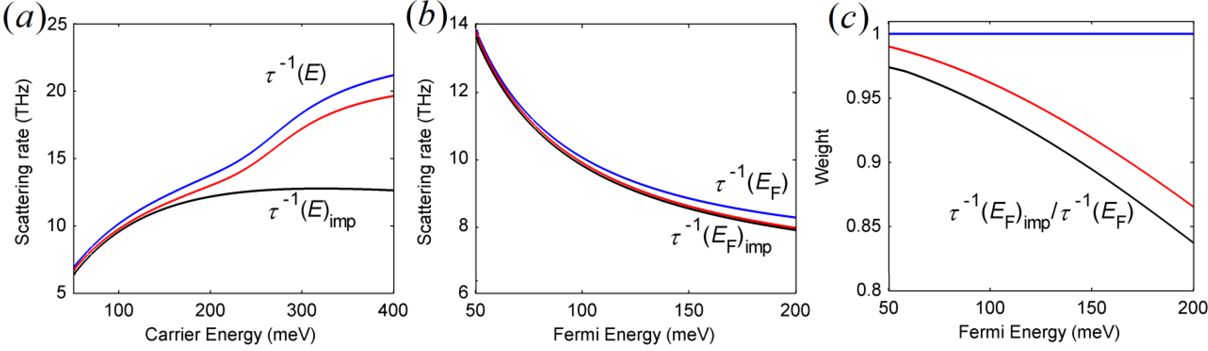
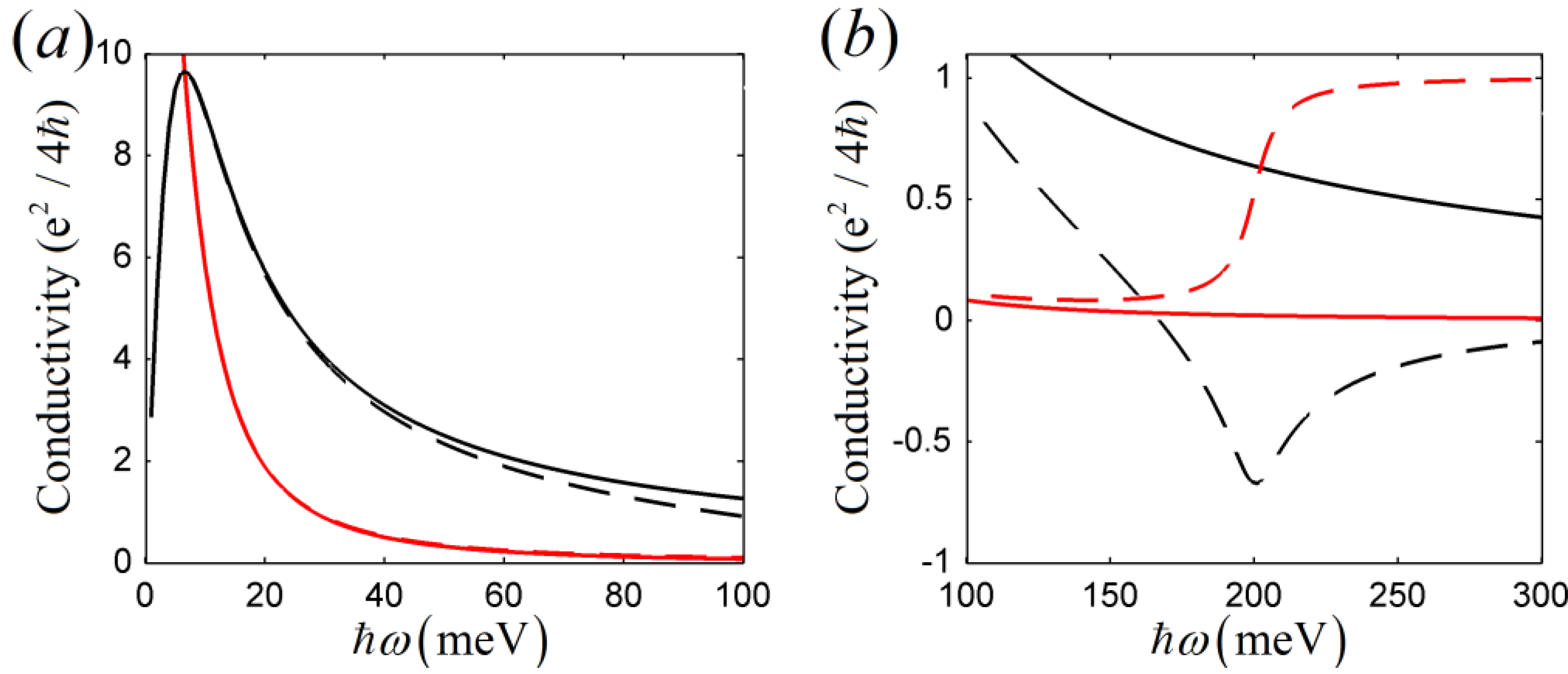
3. Optical Conductivity
3.1. Drude Model

 to obtain an analytical expression [33]:
 ≅ τ−1 (EF) and Equation (7) becomes the familiar simple Drude model σ0/(1 − iωτoff) with σ0 = e2EFτeff / πħ2, which is commonly used in fitting the experimental data. If the condition μ ˃˃ kBT is not valid, has to be calculated numerically. Nevertheless, with EF ≥ 100meV and T = 300 K , it has been shown that is a weak function of frequency, and ≅ τ−1 (EF) is a fairly good approximation for Equation (7) [33].
3.2. RPA Model


 ; sgn(x) = 1 if x ≤ 0 and −1 otherwise. Equation (9) is identical to Equation (7) of Reference [42] in a slightly different form. Apparently, by setting τ−1 (EF) → 0 for ωγ → ω, Equation (9) reduces to the collisionless results in References [40,41]. To comply with local electron conservation, Equation (9) needs to be modified to [43,44]


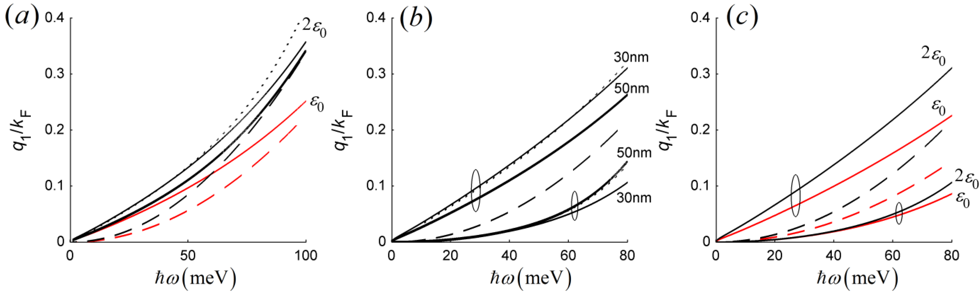
4. Plasmon Dispersion


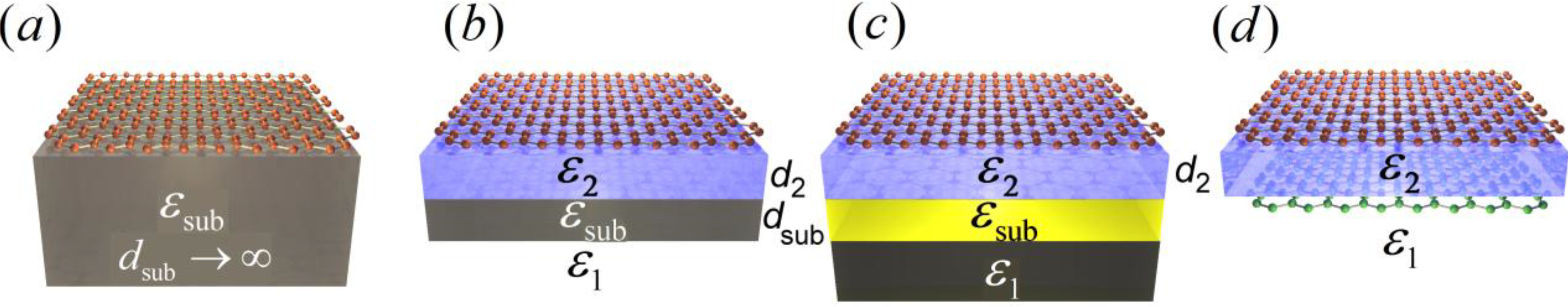
4.1. Graphene on A Polar Substrate


4.2. Graphene on A Metal Substrate

4.3. Double-Layer Graphene


5. Conclusions
Acknowledgments
Conflicts of Interest
References
- Morozov, S.V.; Novoselov, K.S.; Katsnelson, M.I.; Schedin, F.; Elias, D.C.; Jaszczak, J.A.; Geim, A.K. Giant intrinsic carrier mobilities in graphene and its bilayer. Phys. Rev. Lett. 2008, 100, 016602. [Google Scholar] [CrossRef]
- Christensen, J.; Manjavacas, A.; Thongrattanasiri, S.; Koppens, F.H.L.; de Abajo, F.J.G. Graphene plasmon waveguiding and hybridization in individual and paired nanoribbons. ACS Nano 2011, 6, 431–440. [Google Scholar]
- Yan, H.; Low, T.; Zhu, W.; Wu, Y.; Freitag, M.; Li, X.; Guinea, F.; Avouris, P.; Xia, F. Damping pathways of mid-infrared plasmons in graphene nanostructures. Nat. Photonics 2013, 7, 394–399. [Google Scholar] [CrossRef]
- Ju, L.; Geng, B.; Horng, J.; Girit, C.; Martin, M.; Hao, Z.; Bechtel, H.A.; Liang, X.; Zettl, A.; Shen, Y.R.; et al. Graphene plasmonics for tunable terahertz metamaterials. Nat. Nanotechnol. 2011, 6, 630–634. [Google Scholar] [CrossRef]
- Zhan, T.R.; Zhao, F.Y.; Hu, X.H.; Liu, X.H.; Zi, J. Band structure of plasmons and optical absorption enhancement in graphene on subwavelength dielectric gratings at infrared frequencies. Phys. Rev. B 2012, 86, 165416. [Google Scholar]
- Bludov, Y.V.; Peres, N.M.R.; Vasilevskiy, M.I. Graphene-based polaritonic crystal. Phys. Rev. B 2012, 85, 245409. [Google Scholar] [CrossRef]
- Gu, X.; Lin, I.T.; Liu, J.-M. Extremely confined terahertz surface plasmon-polaritons in graphene-metal structures. Appl. Phys. Lett. 2013, 103, 071103. [Google Scholar] [CrossRef]
- Popov, V.V.; Polischuk, O.V.; Davoyan, A.R.; Ryzhii, V.; Otsuji, T.; Shur, M.S. Plasmonic terahertz lasing in an array of graphene nanocavities. Phys. Rev. B 2012, 86, 195437. [Google Scholar] [CrossRef]
- Fei, Z.; Rodin, A.S.; Gannett, W.; Dai, S.; Regan, W.; Wagner, M.; Liu, M.K.; McLeod, A.S.; Dominguez, G.; Thiemens, M.; et al. Electronic and plasmonic phenomena at graphene grain boundaries. Nat. Nanotechnol. 2013, 8, 821–825. [Google Scholar] [CrossRef]
- Niu, J.; Shin, Y.J.; Lee, Y.; Ahn, J.-H.; Yang, H. Graphene induced tunability of the surface plasmon resonance. Appl. Phys. Lett. 2012, 100, 061116. [Google Scholar] [CrossRef]
- Farhat, M.; Guenneau, S.; Bağcı, H. Exciting graphene surface plasmon polaritons through light and sound interplay. Phys. Rev. Lett. 2013, 111, 237404. [Google Scholar] [CrossRef]
- Liu, Y.; Willis, R.F. Plasmon-phonon strongly coupled mode in epitaxial graphene. Phys. Rev. B 2010, 81, 081406. [Google Scholar] [CrossRef]
- Politano, A.; Marino, A.R.; Formoso, V.; Farías, D.; Miranda, R.; Chiarello, G. Evidence for acoustic-like plasmons on epitaxial graphene on Pt(111). Phys. Rev. B 2011, 84, 033401. [Google Scholar]
- Fei, Z.; Andreev, G.O.; Bao, W.; Zhang, L.M.; McLeod, S.A.; Wang, C.; Stewart, M.K.; Zhao, Z.; Dominguez, G.; Thiemens, M.; et al. Infrared nanoscopy of dirac plasmons at the graphene–SiO2 interface. Nano Lett. 2011, 11, 4701–4705. [Google Scholar] [CrossRef]
- Lin, I.-T.; Liu, J.-M. Coupled surface plasmon modes of graphene in close proximity to a plasma layer. Appl. Phys. Lett. 2013, 103, 201104. [Google Scholar] [CrossRef]
- Wang, B.; Zhang, X.; Yuan, X.; Teng, J. Optical coupling of surface plasmons between graphene sheets. Appl. Phys. Lett. 2012, 100, 131111. [Google Scholar] [CrossRef]
- Profumo, R.E.V.; Asgari, R.; Polini, M.; MacDonald, A.H. Double-layer graphene and topological insulator thin-film plasmons. Phys. Rev. B 2012, 85, 085443. [Google Scholar]
- Stauber, T.; Gómez-Santos, G. Plasmons in layered structures including graphene. New J. Phys. 2012, 14, 105018. [Google Scholar] [CrossRef]
- Correas-Serrano, D.; Gomez-Diaz, J.S.; Perruisseau-Carrier, J.; Alvarez-Melcon, A. Spatially dispersive graphene single and parallel plate waveguides: Analysis and circuit model. IEEE Trans. Microw. Theory Tech. 2013, 61, 4333–4344. [Google Scholar] [CrossRef]
- Hwang, E.H.; Adam, S.; Das Sarma, S. Carrier transport in two-dimensional graphene layers. Phys. Rev. Lett. 2007, 98, 186806. [Google Scholar] [CrossRef]
- Chen, J.H.; Jang, C.; Adam, S.; Fuhrer, M.S.; Williams, E.D.; Ishigami, M. Charged-impurity scattering in graphene. Nat. Phys. 2008, 4, 377–381. [Google Scholar]
- Chen, J.-H.; Jang, C.; Xiao, S.; Ishigami, M.; Fuhrer, M.S. Intrinsic and extrinsic performance limits of graphene devices on SiO2. Nat. Nanotechnol. 2008, 3, 206–209. [Google Scholar] [CrossRef]
- Tan, Y.W.; Zhang, Y.; Bolotin, K.; Zhao, Y.; Adam, S.; Hwang, E.H.; Das Sarma, S.; Stormer, H.L.; Kim, P. Measurement of scattering rate and minimum conductivity in graphene. Phys. Rev. Lett. 2007, 99, 246803. [Google Scholar] [CrossRef]
- Tanabe, S.; Sekine, Y.; Kageshima, H.; Nagase, M.; Hibino, H. Carrier transport mechanism in graphene on SiC(0001). Phys. Rev. B 2011, 84, 115458. [Google Scholar]
- Zou, K.; Hong, X.; Keefer, D.; Zhu, J. Deposition of high-quality HfO2 on graphene and the effect of remote oxide phonon scattering. Phys. Rev. Lett. 2010, 105, 126601. [Google Scholar] [CrossRef]
- Hwang, E.H.; Das Sarma, S. Acoustic phonon scattering limited carrier mobility in two-dimensional extrinsic graphene. Phys. Rev. B 2008, 77, 115449. [Google Scholar] [CrossRef]
- Castro, E.V.; Ochoa, H.; Katsnelson, M.I.; Gorbachev, R.V.; Elias, D.C.; Novoselov, K.S.; Geim, A.K.; Guinea, F. Limits on charge carrier mobility in suspended graphene due to flexural phonons. Phys. Rev. Lett. 2010, 105, 266601. [Google Scholar] [CrossRef]
- Dean, C.R.; Young, A.F.; Meric, I.; Lee, C.; Wang, L.; Sorgenfrei, S.; Watanabe, K.; Taniguchi, T.; Kim, P.; Shepard, K.L.; et al. Boron nitride substrates for high-quality graphene electronics. Nat. Nanotechnol. 2010, 5, 722–726. [Google Scholar] [CrossRef]
- Hwang, E.H.; Das Sarma, S. Screening-induced temperature-dependent transport in two-dimensional graphene. Phys. Rev. B 2009, 79, 165404. [Google Scholar] [CrossRef]
- Wang, S.Q.; Mahan, G.D. Electron scattering from surface excitations. Phys. Rev. B 1972, 6, 4517–4524. [Google Scholar] [CrossRef]
- Konar, A.; Fang, T.; Jena, D. Effect of high-κ gate dielectrics on charge transport in graphene-based field effect transistors. Phys. Rev. B 2010, 82, 115452. [Google Scholar]
- Lin, I.T.; Liu, J.-M. Surface polar optical phonon scattering of carriers in graphene on various substrates. Appl. Phys. Lett. 2013, 103, 081606. [Google Scholar] [CrossRef]
- Lin, I.T.; Liu, J.M. Terahertz frequency-dependent carrier scattering rate and mobility of monolayer and AA-stacked multilayer graphene. IEEE J. Sel. Top. Quantum Electron. 2014, 20, 8400108. [Google Scholar]
- Fratini, S.; Guinea, F. Substrate-limited electron dynamics in graphene. Phys. Rev. B 2008, 77, 195415. [Google Scholar] [CrossRef]
- Malard, L.M.; Pimenta, M.A.; Dresselhaus, G.; Dresselhaus, M.S. Raman spectroscopy in graphene. Phys. Rep. 2009, 473, 51–87. [Google Scholar]
- Piscanec, S.; Lazzeri, M.; Mauri, F.; Ferrari, A.C.; Robertson, J. Kohn anomalies and electron-phonon interactions in graphite. Phys. Rev. Lett. 2004, 93, 185503. [Google Scholar] [CrossRef]
- Yao, Z.; Kane, C.L.; Dekker, C. High-field electrical transport in single-wall carbon nanotubes. Phys. Rev. Lett. 2000, 84, 2941–2944. [Google Scholar] [CrossRef]
- Stauber, T.; Peres, N.M.R.; Guinea, F. Electronic transport in graphene: A semiclassical approach including midgap states. Phys. Rev. B 2007, 76, 205423. [Google Scholar] [CrossRef]
- Bohm, D.; Pines, D. A collective description of electron interactions. I. magnetic interactions. Phys. Rev. 1951, 82, 625–634. [Google Scholar] [CrossRef]
- Hwang, E.H.; Das Sarma, S. Dielectric function, screening, and plasmons in two-dimensional graphene. Phys. Rev. B 2007, 75, 205418. [Google Scholar] [CrossRef]
- Wunsch, B.; Stauber, T.; Sols, F.; Guinea, F. Dynamical polarization of graphene at finite doping. New J. Phys. 2006, 8, 318. [Google Scholar] [CrossRef]
- Pyatkovskiy, P.K. Dynamical polarization, screening, and plasmons in gapped graphene. J. Phys. Condens. Matter 2009, 21, 025506. [Google Scholar] [CrossRef]
- Jablan, M.; Buljan, H.; Soljačić, M. Plasmonics in graphene at infrared frequencies. Phys. Rev. B 2009, 80, 245435. [Google Scholar] [CrossRef]
- Mermin, N.D. Lindhard dielectric function in the relaxation-time approximation. Phys. Rev. B 1970, 1, 2362–2363. [Google Scholar] [CrossRef]
- Koppens, F.H.L.; Chang, D.E.; de Abajo, F.J.G. Graphene plasmonics: A platform for strong light–matter interactions. Nano Lett. 2011, 11, 3370–3377. [Google Scholar] [CrossRef]
- West, P.R.; Ishii, S.; Naik, G.V.; Emani, N.K.; Shalaev, V.M.; Boltasseva, A. Searching for better plasmonic materials. Laser Photonics Rev. 2010, 4, 795–808. [Google Scholar] [CrossRef]
- Gan, C.H.; Chu, H.S.; Li, E.P. Synthesis of highly confined surface plasmon modes with doped graphene sheets in the midinfrared and terahertz frequencies. Phys. Rev. B 2012, 85, 125431. [Google Scholar] [CrossRef]
- Zeman, E.J.; Schatz, G.C. An accurate electromagnetic theory study of surface enhancement factors for silver, gold, copper, lithium, sodium, aluminum, gallium, indium, zinc, and cadmium. J. Phys. Chem. 1987, 91, 634–643. [Google Scholar] [CrossRef]
© 2014 by the authors; licensee MDPI, Basel, Switzerland. This article is an open access article distributed under the terms and conditions of the Creative Commons Attribution license (http://creativecommons.org/licenses/by/3.0/).
Share and Cite
Lin, I.-T.; Lai, Y.-P.; Wu, K.-H.; Liu, J.-M. Terahertz Optoelectronic Property of Graphene: Substrate-Induced Effects on Plasmonic Characteristics. Appl. Sci. 2014, 4, 28-41. https://doi.org/10.3390/app4010028
Lin I-T, Lai Y-P, Wu K-H, Liu J-M. Terahertz Optoelectronic Property of Graphene: Substrate-Induced Effects on Plasmonic Characteristics. Applied Sciences. 2014; 4(1):28-41. https://doi.org/10.3390/app4010028
Chicago/Turabian StyleLin, I-Tan, Yi-Ping Lai, Kuang-Hsiung Wu, and Jia-Ming Liu. 2014. "Terahertz Optoelectronic Property of Graphene: Substrate-Induced Effects on Plasmonic Characteristics" Applied Sciences 4, no. 1: 28-41. https://doi.org/10.3390/app4010028
APA StyleLin, I.-T., Lai, Y.-P., Wu, K.-H., & Liu, J.-M. (2014). Terahertz Optoelectronic Property of Graphene: Substrate-Induced Effects on Plasmonic Characteristics. Applied Sciences, 4(1), 28-41. https://doi.org/10.3390/app4010028