1. Introduction
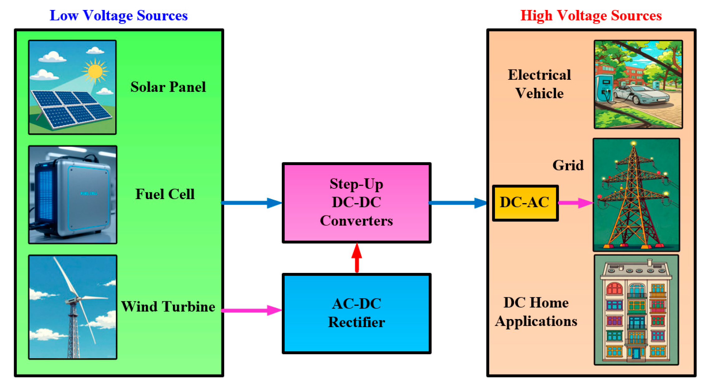
Over the last ten years, priorities across the global energy sector have increasingly centered on cutting greenhouse gas emissions and expanding the contribution of renewable resources to electricity production. As illustrated schematically in
Figure 1, renewables are now broadly viewed as the leading pathway for phasing out conventional, fossil-fuel-based generation. Among these options, photovoltaic (PV) technology has become especially prominent because sunlight is abundant and widely accessible, solar power is sustainable over the long term, and PV systems generally impose a relatively small environmental burden [
1].
From an engineering perspective, a major challenge is that photovoltaic arrays and fuel cells naturally produce low-magnitude DC voltages, which cannot be connected to the grid without additional conditioning. To address this mismatch, a high step-up DC–DC conversion stage is typically introduced. Such converters elevate the modest DC output of the renewable source to a level suitable for subsequent power processing and eventual grid integration [
2,
3,
4]. As a result, they are a core element of contemporary renewable-energy systems, enabling cleaner electricity production and supporting worldwide efforts to curb air pollution, reduce environmental harm, and lessen the climate impacts linked to fossil fuel dependence [
5,
6].
To achieve high output voltages and step up the naturally low DC levels delivered by clean sources such as photovoltaic (PV) arrays, designers have incorporated a wide range of specialized step-up strategies into boost-type DC–DC converter structures [
7,
8,
9]. Frequently adopted solutions include switched-capacitor (SC) and switched-inductor (SL) networks, active switched-inductor (A-SL) techniques, converter topologies employing coupled inductors (CIs), voltage-lift and voltage-multiplier (VM) principles, and both interleaved and multi-stage (cascaded) architectures [
10,
11,
12,
13]. In many reported designs, two or more of these concepts are also merged into hybrid forms to further increase voltage gain and enhance overall converter performance [
14,
15,
16,
17,
18].
Within the family of high step-up converters created by blending the above techniques, quadratic topologies are particularly attractive because they can produce exceptionally high voltage conversion ratios [
19,
20,
21,
22,
23,
24]. This advantage stems from the appearance of the (1 − D)
2 term in the denominator of their VG expression. In [
25], a quadratic step-up circuit that integrates switched-inductor and switched-capacitor networks is proposed, achieving a relatively high step-up ratio. However, since one of the capacitors is directly linked to the input source, the configuration draws a pulsating input current, which is an undesirable characteristic for many applications. In another topology reported in [
26], switched-inductor and switched-capacitor cells are again combined, but this time two series-connected capacitors are employed to control the converter’s output voltage. This arrangement succeeds in lowering the VS on the capacitors and ensures a continuous input current. However, the main switch is still exposed to a voltage stress equal to the full output voltage. Although the converters proposed in [
25,
26] all exhibit quadratic voltage gain characteristics, the elevated VS on the switch contributes to significant conduction and switching losses. As a result, these configurations are not appropriate for applications requiring very high output voltages.
In [
27], a family of quadratic configurations is presented that combines coupled inductors with voltage multiplier stages while aiming to reduce device voltage stress. Although these configurations can acquire a high step-up ratio, they are affected by considerable input current ripple, which constrains their applicability in DC microgrid environments. In [
28], another quadratic topology based on a CI with two cascaded boosting stages is introduced to obtain large voltage gain; however, this structure incurs noticeable power losses in the input diodes and is characterized by a high input current.
A different quadratic architecture with low device voltage stress is designed in [
29]. Although it achieves a high voltage step-up, the series connection between the coupled-inductor primary winding and the input DC source leads to pronounced ripple in the input current, which in turn places extra stress on the source. High-gain topologies with improved input-current ripple characteristics are presented in [
30,
31], where two- or three-winding CIs are integrated with voltage-multiplier cells. This approach offers additional design flexibility, allowing the conversion ratio to be tuned over a broad range. However, these converters still suffer from high voltage stress on the main switch and significant current stress in the input diodes.
References [
32,
33,
34] propose quadratic converter designs that combine coupled inductors with switched-capacitor networks in order to obtain high voltage gains. A key limitation of these structures is the large capacitor peak currents, which can increase power dissipation and worsen electromagnetic interference. In [
35], a quadratic impedance-source converter augmented with a CI is presented, providing strong step-up performance with a comparatively low component count. Even so, the semiconductor devices in this topology continue to experience considerable voltage stress.
In [
21], a quadratic boost converter incorporating a SEPIC-like stage is proposed and examined. The converter achieves a high conversion ratio while keeping the input-current ripple small, which helps overcome issues commonly faced in DC microgrid environments. However, the additional passive parts—most notably the coupling capacitor—add resistive and reactive losses, which ultimately reduce efficiency.
Reference [
36] introduces a quadratic topology featuring soft switching, a continuous input current, and reduced voltage stress on the semiconductor devices. While this approach successfully alleviates voltage-stress concerns, it relies on a comparatively high component count, particularly in magnetic components. This increases cost and reduces power density, making practical implementation less attractive.
Driven by the strengths and limitations of current high boost configuration designs, this article describes a novel quadratic ultra-high boost DC–DC topology tailored for renewable energy systems. The proposed configuration provides two independent degrees of freedom for adjusting the VG, namely the duty cycles of the power switches and the turns ratio of the CI, which gives the designer considerable flexibility. Unlike many conventional high-gain converters, the suggested configuration can achieve a substantial step-up ratio without being restricted to severe duty-cycle values, allowing the duty cycle to vary over the entire range from 0 to 1. Furthermore, it can deliver an ultra-high output voltage even at relatively small duty cycles, which helps reduce conduction losses. Another important advantage is the low VS on the MOSFETs, enabling the employment of low-voltage-rating switches with small on-state resistance, thereby minimizing conduction losses and enhancing overall efficiency. The topology also features a continuous input current with low ripple, which is highly favorable when interfacing with vulnerable renewable sources such as PV modules. In addition, the converter operates with two active power switches driven synchronously and maintains a common ground capability, simplifying system integration and control. Finally, the proposed structure ensures soft-switching operation for diodes D3 and D4, effectively reducing switching losses and mitigating electromagnetic interference.
2. Proposed Configuration and Operation Modes
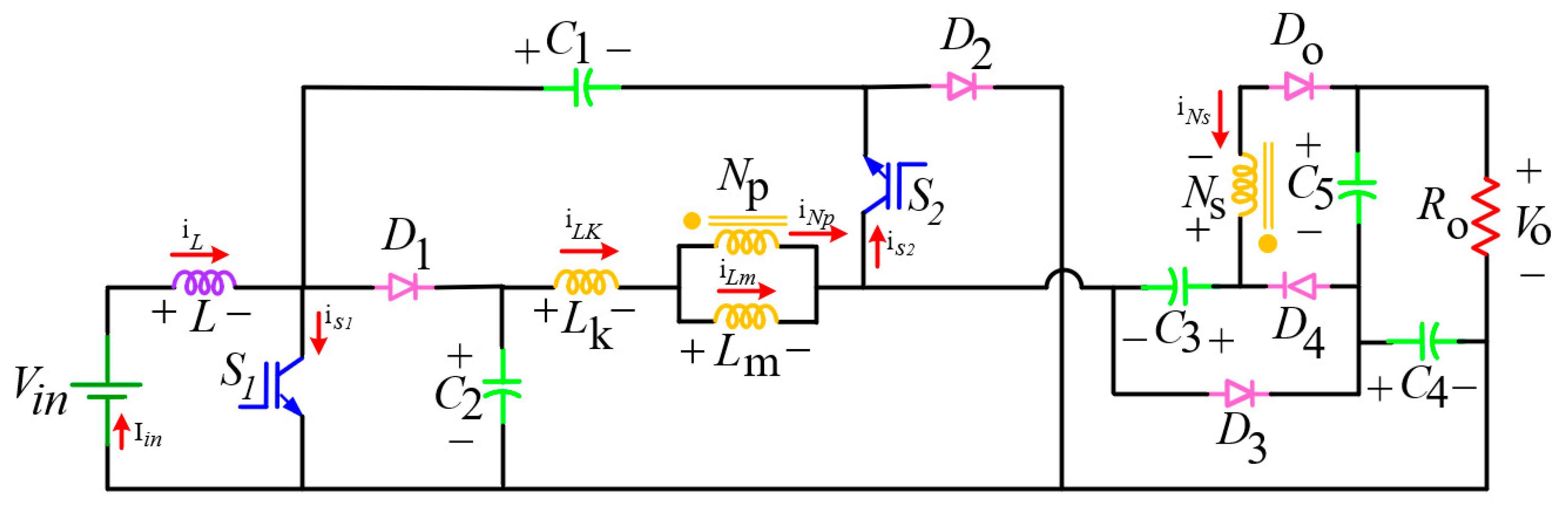
The proposed quadratic topology depicted in
Figure 2 illustrates the layout of the new converter. It incorporates an input inductor L, two active switches S
1 and S
2, five capacitors (C
1–C
5), five diodes (D
1–D
4 and D
O) and a CI composed of two windings: a primary winding N
P and a secondary winding N
S. The turns ratio of this CI is expressed as n = N
S/N
P, and the coupling coefficient is defined as k = L
m/(L
m + L
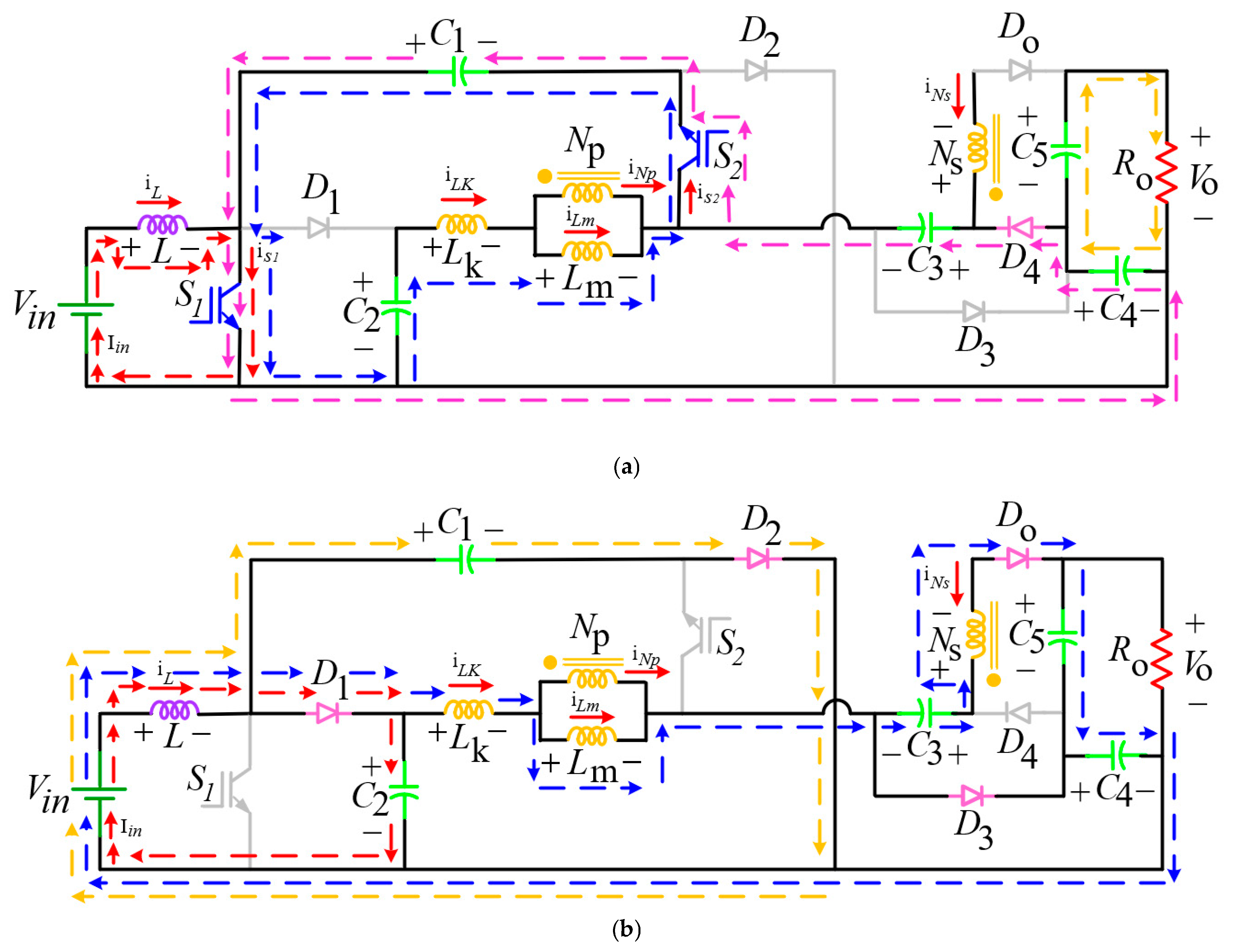
k). The configuration functions under continuous conduction mode (CCM), and its switching period can be separated into two operating intervals, illustrated in
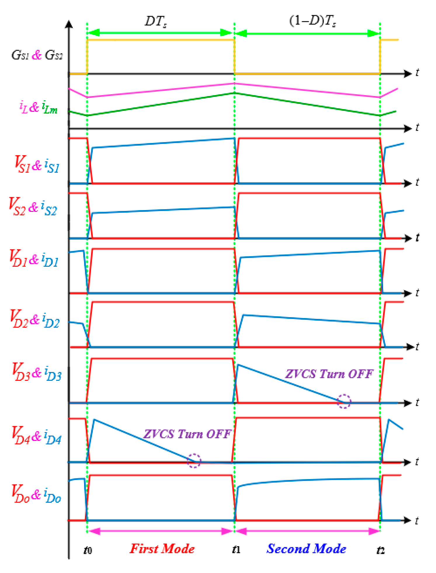
Figure 3. The corresponding key voltage and current waveforms of the circuit elements are shown in
Figure 4.
First Mode: In this mode, both switches S
1 and S
2 are in the ON state, and diode D
4 conducts, while all other diodes remain reverse-biased. At t
0 = 0, diode D
3 turns off under zero-voltage and zero-current switching (ZVCS) conditions. The magnetizing inductance L
m is energized through the loop composed of C
2, L
m, S
2, C
1, and S
1, causing the magnetizing current i
Lm to increase linearly and simultaneously discharging capacitors C
1 and C
2. Concurrently, the input inductor L is energized via the path V
in–L–S
1, resulting in a linear rise of the inductor current i
L. In parallel, capacitor C
3 is charged and C
4 is discharged through the loop formed by C
4, D
4, C
3, S
2, C
1, and S
1, while capacitor C
5 releases energy through the path including C
4, C
5, and the output voltage. Throughout this interval, the voltages and currents in the structure obey Kirchhoff’s Voltage Law (KVL) and Kirchhoff’s Current Law (KCL).
Second Mode: In this operating interval, both power switches are in the OFF state, which causes diodes D
1, D
2, D
3, and D
O to conduct, while diode D
4 is turned off under ZVCS conditions. The magnetizing inductance L
m and the input inductor L release their stored energy through the path V
in → L → D
1 → L
m → C
3 → N
S → D
O → C
5 → C
4. As a result, the currents in L
m and L decrease gradually, capacitor C
3 is discharged, and capacitors C
4 and C
5 are charged along this route. Meanwhile, capacitor C
1 is replenished via the loop V
in → L → C
1 → D
2, and capacitor C
2 is energized along the path V
in → L → D
1 → C
2. The mathematical relations governing this interval can be written as follows.
The volt–second equilibrium condition for inductor L and CI can be formulated as follows:
The steady-state voltages of the capacitors and the output voltage are derived by applying the volt–second balance principle to the input inductor and the coupled inductor under continuous conduction mode. In steady state, the voltages of capacitors C
1 and C
2 are equal, and their value is obtained from the average voltage of the input inductor L using the inductor voltage expressions defined in Equations (3) and (20). By enforcing the zero average voltage condition over one switching period, the voltage of C
1 (and consequently C
2) is determined. The voltage of capacitor C
4 is then derived by applying volt–second balance to the magnetizing inductance L
m using the primary–side voltage relations given in Equations (4) and (22), while noting that the primary voltage V
1 is directly related to the magnetizing inductance voltage according to Equation (1). Based on the obtained values of C
1, C
2, and C
4, the voltage of capacitor C
3 is determined from the circuit relations in the first switching interval using Equations (5) and (22). The voltage of capacitor C
5 is obtained from the circuit relations in the second switching interval using Equations (5) and (23), which include the contribution of the coupled-inductor secondary voltage.
Finally, once the voltages of capacitors C
4 and C
5 are known, the output voltage is obtained from their series combination according to Equation (6).
Ignoring the influence of the coupling coefficient of CI (especially for k = 1), the VG can be written as:
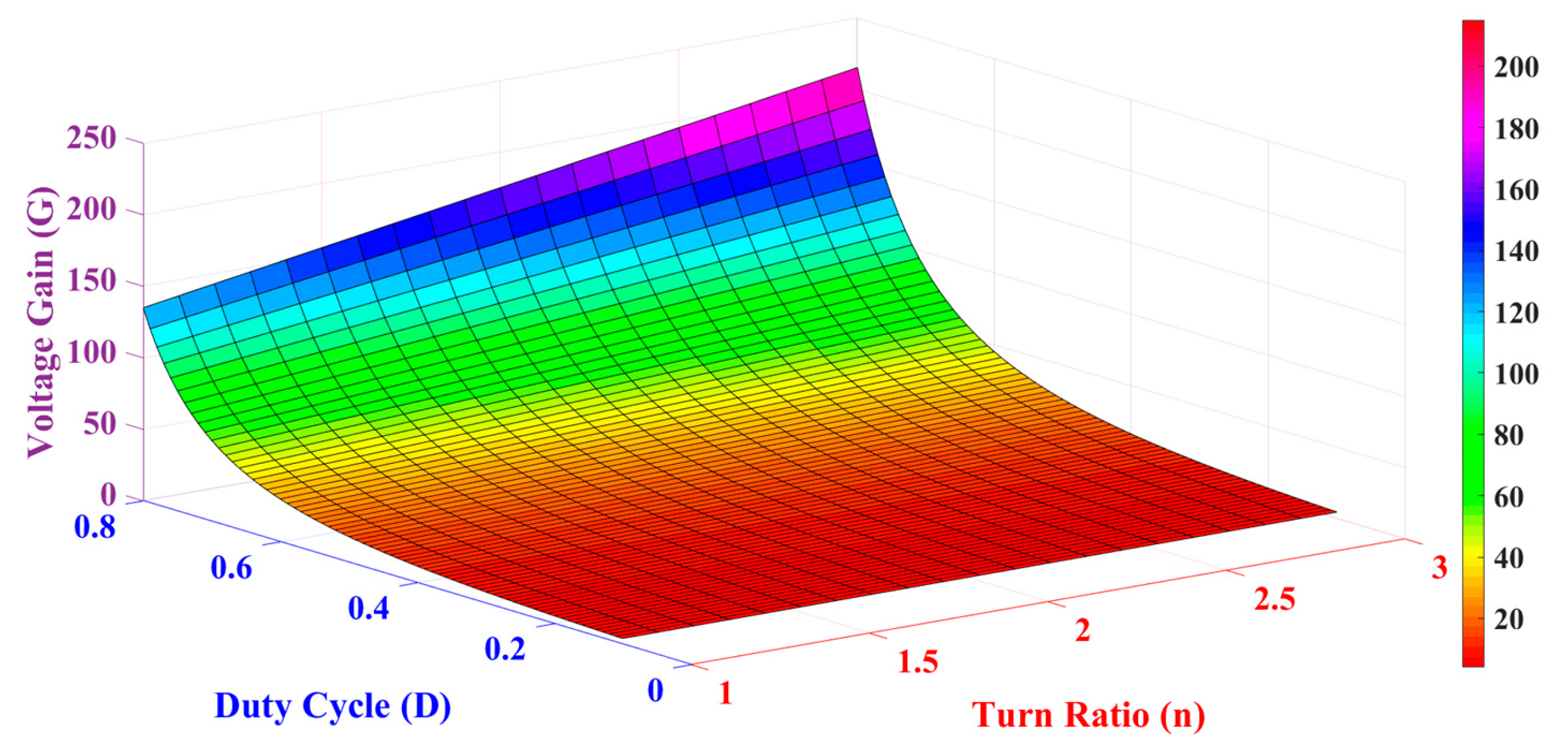
A three-dimensional surface of the configuration gain is displayed in
Figure 5. This plot shows that, for appropriate selections of D and n, the proposed structure can deliver very large step-up ratios, with the voltage gain varying in a quadratic manner.
The VS imposed on the semiconductors in the proposed configuration are determined as follows:
The semiconductor device currents in each switching interval can be described by the following expressions:
The analytical expressions used to evaluate the currents flowing through the input inductor L, the magnetizing inductance L
m, and the primary and secondary windings of the CI are presented below:
Using the equivalent circuits for each functioning mode and enforcing the ampere–second balance condition, the capacitor current relationships are obtained as follows:
The mean current loading of the switches and the diodes is determined by the following expressions:
To precisely evaluate power dissipation in the converter, it is crucial to estimate the root-mean-square (RMS) current of every device. The step-by-step derivation of the RMS currents for each element is given in (61)–(68) below.
For the proposed topology to function in continuous conduction mode, the inductor current i
L must not fall to zero at any time. Accordingly, the minimum values of the inductor current i
L and the current ripple Δ
iL can be written as:
The smallest inductance of L necessary to ensure operation in CCM can be represented as:
To guarantee correct operation, the instantaneous current flowing through the CI must not reach zero. Accordingly, the minimum current through CI and the ripple component Δ
iLm can be expressed as:
The lowest inductance value of L
m that guarantees continuous conduction mode can be obtained using:
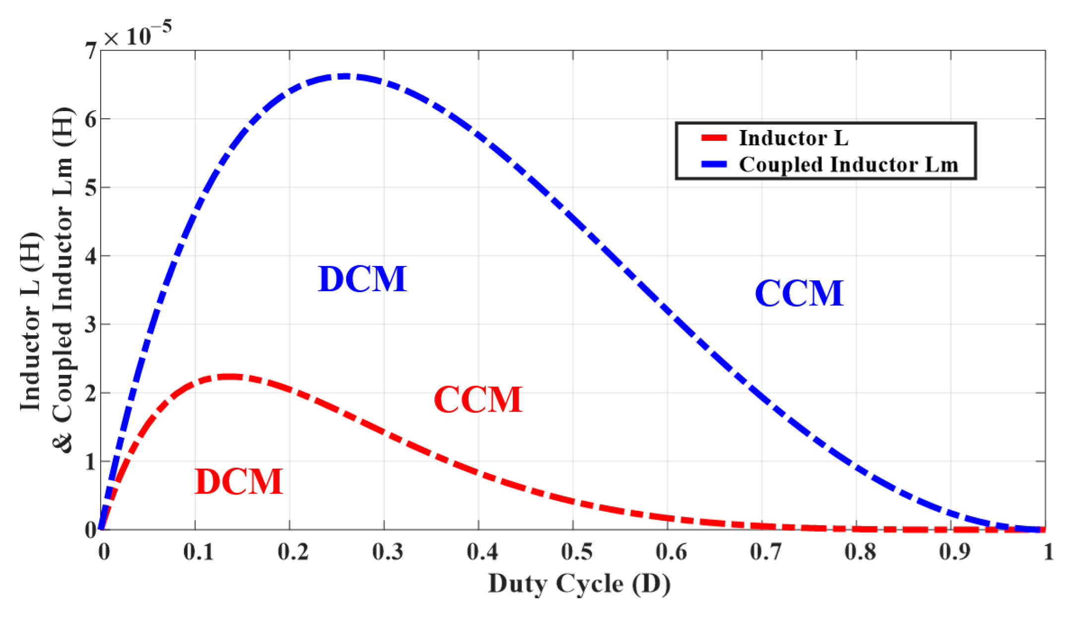
As shown in
Figure 6, the L
min(D) characteristic of the magnetizing inductor L
m lies above that of the input inductor L. This reveals that, under the same input voltage, switching frequency, and load conditions, the magnetizing branch requires a larger inductance value to remain in CCM. Consequently, for the parameter set adopted in this study, L
m transitions into discontinuous conduction mode (DCM) before L, which can be clearly observed in
Figure 6. In addition to being continuous, the input current of the proposed converter exhibits a very low ripple at the rated operating point. For an average input current of approximately 22 A, the peak-to-peak ripple is about 0.5 A, which corresponds to an input current ripple ratio of nearly 2.27%. Such a low ripple level confirms the source-friendly nature of the proposed topology and makes it particularly suitable for PV and fuel-cell applications, where minimizing input current pulsation is essential to reduce source stress, improve operating-point stability, and enhance overall system reliability.
3. Efficiency Calculation
In this section, the study examines the conduction- and switching-related power losses of the proposed system in order to improve its overall performance. The evaluation accounts for the primary elements that contribute to energy dissipation, including the internal resistances of diodes (r
D), semiconductor switches (r
S), magnetic components such as inductors (r
Lm), and capacitors (r
C). The analysis also incorporates the forward voltage drops of both the diodes (V
FD) and the switching devices (V
FS) when determining the total loss profile. With these factors considered, the expressions for conduction losses in the switches and diodes are formulated as:
The switching energy dissipation of the power components, namely the semiconductor switches and diodes, is evaluated by applying the following assessment method:
A comprehensive expression for the total power loss in both switches and diodes, incorporating contributions from conduction and switching mechanisms, can be written as:
The conduction-related power dissipation for capacitors C
1 through C
5 is evaluated using the following expressions:
The overall power loss attributed to the capacitors is expressed through the following formulation:
The formulas employed to quantify the conduction losses of the magnetizing inductance
Lm and the filter inductor
L are presented below:
The power dissipation associated with the inductive components is characterized by the following expressions:
The inductor core loss, represented as PC, is typically provided in units of W/kg. The coefficients α, β, and k, known as the Steinmetz parameters, are usually designated by core fabricators for different magnetic materials. For ferrite cores, the value of α commonly lies between 1 and 2 (1 ≤ α ≤ 2). Using Faraday’s law, the corresponding loss expression can be written as:
Core manufacturers generally supply the cross-sectional area
Ac for their magnetic components. With this parameter available, the peak flux variation
ΔB in the inductors can be specified using the following relationship:
The core-related losses of the inductors are expressed as
PCore = P × M, where
M is the mass of the magnetic core material. Since the peak flux density is given by
Bm = ΔB/2, the resulting core loss can be calculated using the following equation:
An ETD 49/25/16 magnetic core is chosen for the inductors, with the associated Steinmetz coefficients given as k = 4.124 × 10
−5, α = 1.72, and β = 2.76. Using these parameters, the total power loss for the high boost structure can be determined from the following expression:
The efficiency of the suggested topology, denoted by
η, is specified according to the following expression:
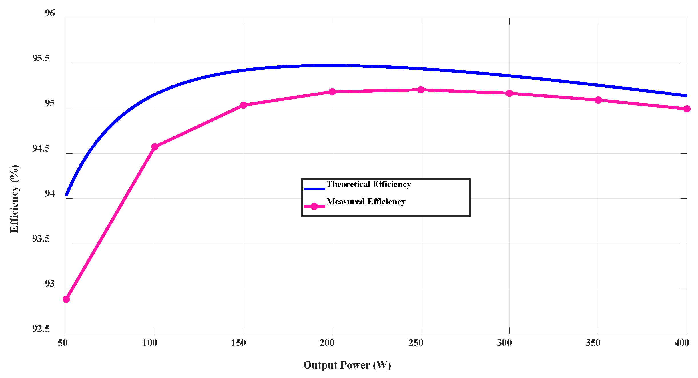
Using the formulations provided in Equations (88)–(115), the analytical efficiency of the suggested design is derived.
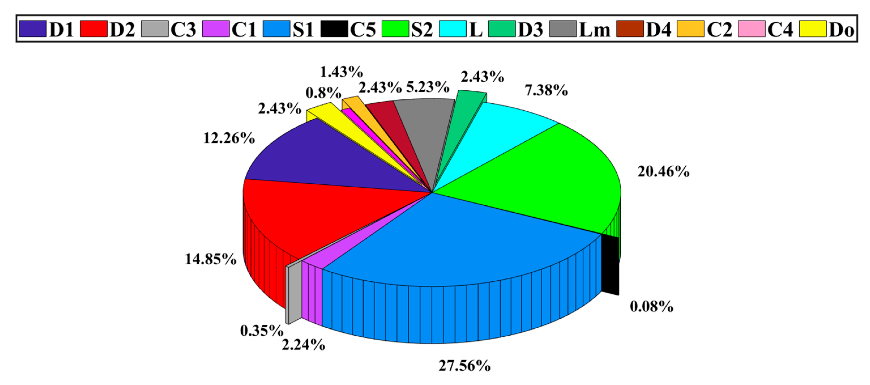
Figure 7 compares the predicted efficiency with the experimentally measured values across varying output power levels. A detailed distribution of individual component losses is shown in
Figure 8, where it is evident that switch S
1 incurs the greatest portion of the losses, while capacitor C
5 contributes the least.
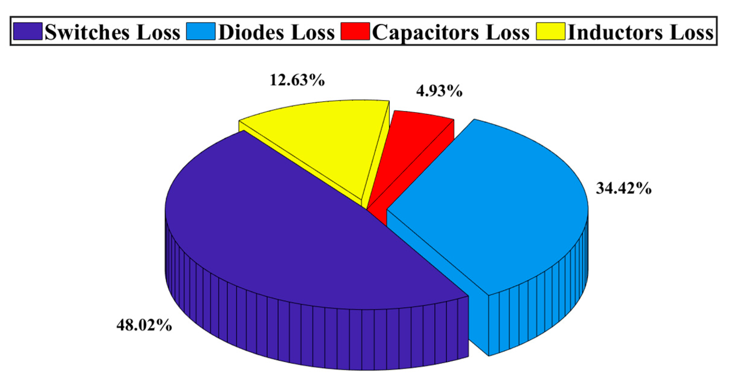
Figure 9 further presents the calculated loss distribution among the two switches, five diodes, five capacitors, and two inductors, revealing that the semiconductor elements (switches and diodes) are responsible for the majority of the total dissipation, approximately 82.44%, with the passive components playing a substantially smaller role. In
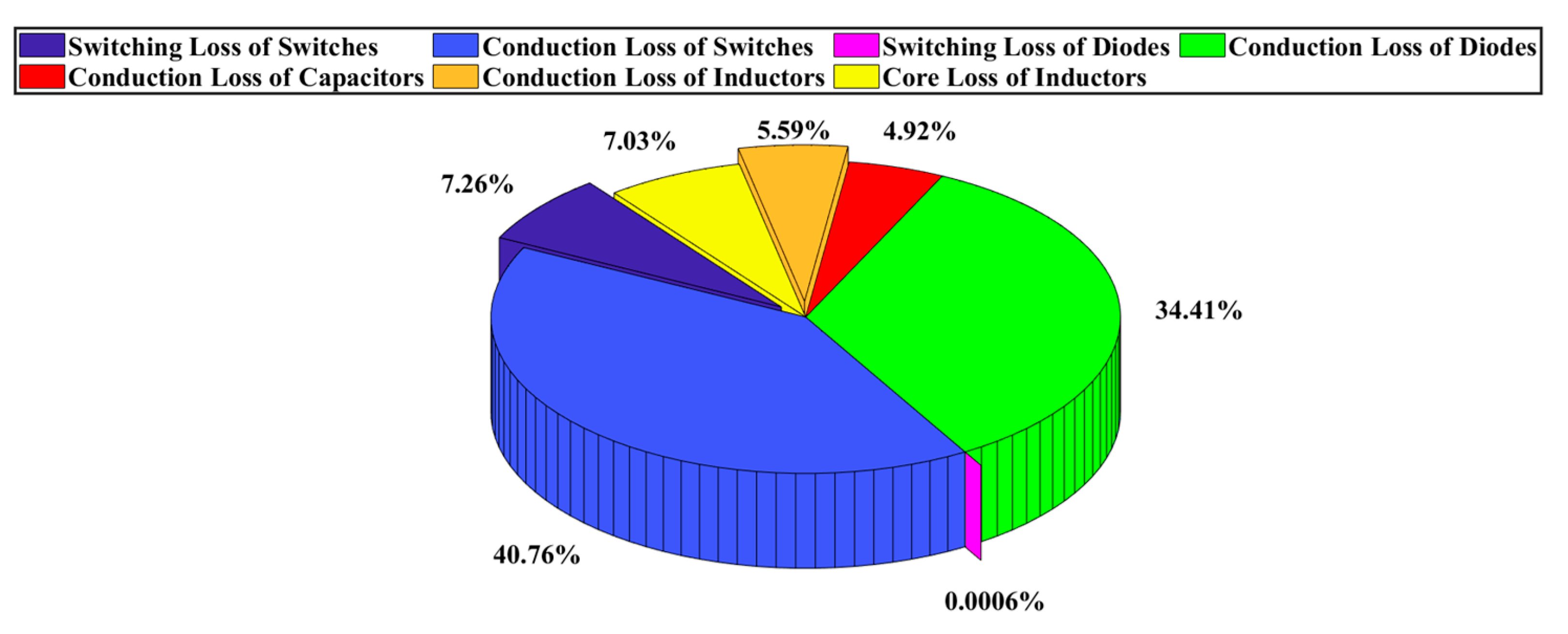
Figure 10, losses are categorized into conduction losses of switches, diodes, capacitors, and inductors; switching losses of switches and diodes; and magnetic core losses. The analysis indicates that switching losses are relatively minor compared with conduction and core losses.
5. Small Signal Modeling
In this section, the evaluation is executed under the presumption that all semiconductor devices, inductors, and capacitors operate ideally. To correctly isolate the state variables for each switching mode, non-idealities are incorporated by representing the inductors with series resistances r
L and the capacitors with series resistances r
C. The state-space averaging technique is then utilized to derive both the averaged and small-signal models. This procedure requires formulating the system dynamics for each mode and computing their weighted average over one switching cycle, derived from each interval. For the two switching submodes, the corresponding system equations are obtained using Equation (123), with Z = 1 and Z = 2.
The control method employed for the proposed configuration utilizes a pole-placement approach, relying on the small-signal model obtained from the state-space averaged representation. In this framework, each state variable and control input is separated into two components: a steady-state term
and a disturbance or dynamic term
.
Following this procedure to arrive at the state-space averaged representation while ignoring second-order perturbation terms produces the small-signal model corresponding to the proposed structure.
The state variables
, control inputs
, and output quantities y are defined as follows:
Using the pole-placement technique, the closed-loop poles can be situated at any desired locations, as long as the system retains full state control capability. The control capability matrix for the proposed circuit is given by:
If the controllability matrix
has a rank of 7, which corresponds to the count of state variables
, the system is considered fully regulatable. In this scenario, two extra integral states are introduced as follows:
With the integral states included, the state-space representation and the corresponding output formulas are reformulated as follows:
In this representation, r(t) denotes the reference input vector, which is defined as follows:
Based on Equation (131), the updated forms of matrices
and
are expressed as follows:
For the system described in Equation (131), the corresponding controllability matrix is given by:
When
is full rank, the system in Equation (131) is entirely regulatable provided that the controllability matrix M has rank n + m, where n designates the count of state variables
and m represents the count of outputs y. Under these conditions, the gain matrix K is obtained using:
The feedback gain matrices K
x and K
q are expressed as follows:
By merging Equation (135) with Equation (131), the emerging equation becomes:
Now we are faced with the problem of finding the controlling signal via state feedback gain matrix K so that the closed-loop system eigenvalues are placed at the desired locations. There are several methods to determine the system controller matrix K = [Kx, Kq]. The control systems toolbox of the MATLAB software provides a useful pole-placement function, which inputs the system (137) and the desired eigenvalues locations to find the state feedback gain matrixes.
To stabilize the system, the values of K
x and K
q are determined as follows:
By using MATLAB software, the pole and zero placements for
Equation (139) can be expressed as:
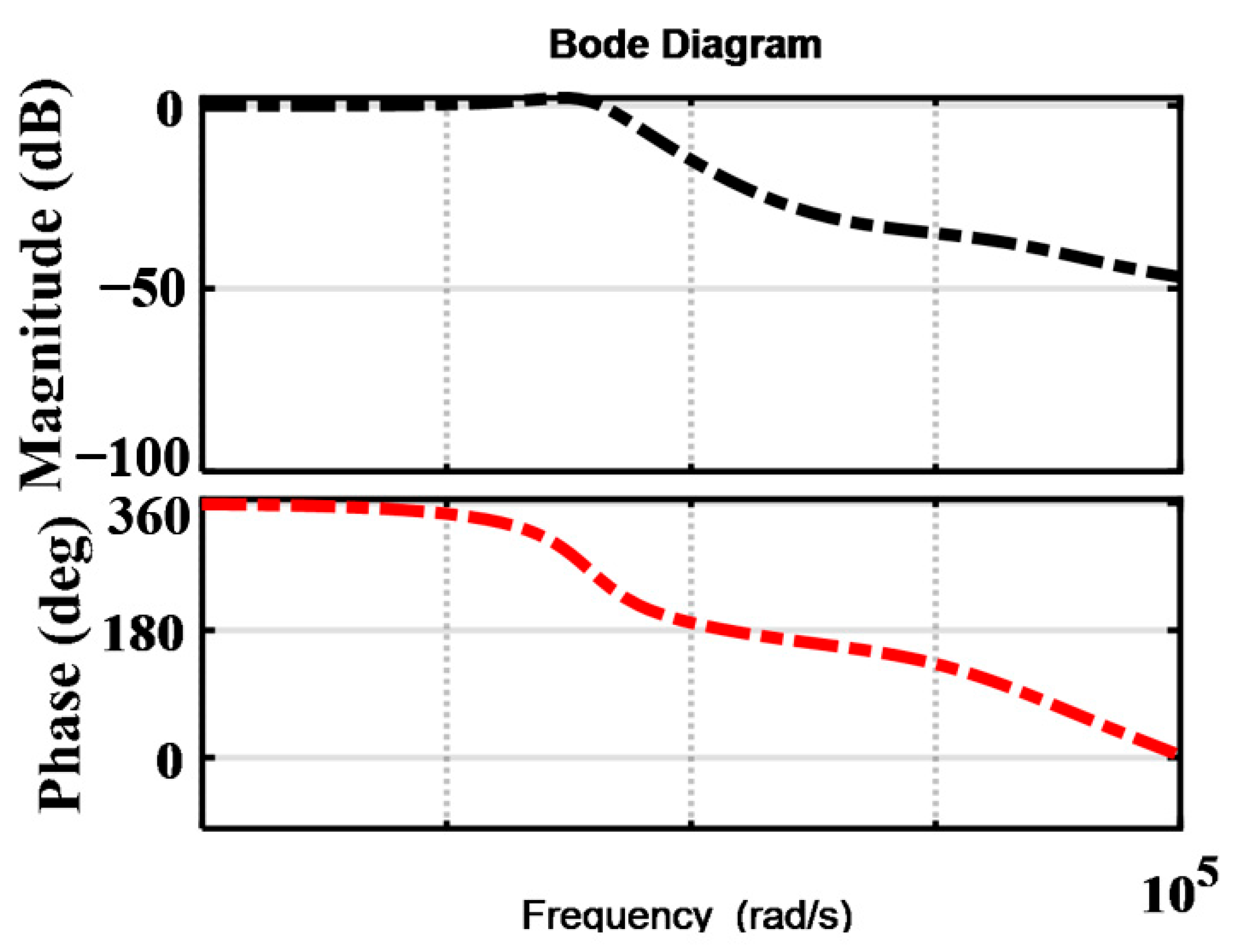
To acquire the specified Gain Margin (GM ≥ 10) and Phase Margin (60° ≤ PM ≤ 80°), a trial-and-error approach is implemented to adjust the sites of the closed-loop poles. Using this method, the Bode plot of the control method for the proposed converter is shown in
Figure 11. As seen in
Figure 11, the gain margin for the inductor L
m exceeds 10 (GM(i
Lm) > 10), and the phase margin for the closed-loop path of i
Lm is 70.5892, which is within the desired range.
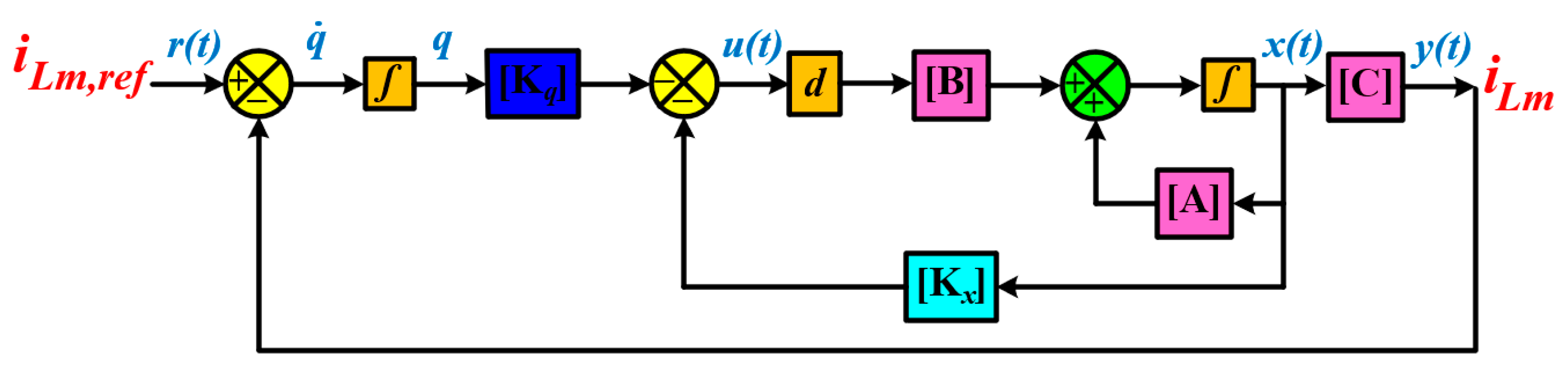
Figure 12 and
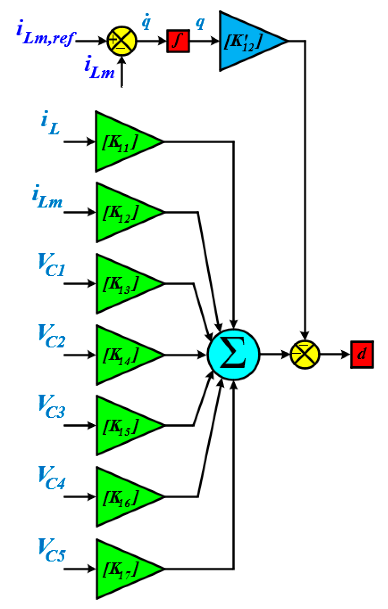
Figure 13 present the block diagram of the pole-placement control method and the current regulation loop for the CI, respectively. The output voltage is sensed and compared with the reference to generate an error signal, which is processed by the controller (compensator) to produce the duty-ratio command. This duty command is then applied to the PWM generation block to drive the switches, while the feedback path closes the loop and ensures regulation against input and load variations. The diagram therefore clarifies the signal flow from reference, error computation, and controller output to PWM actuation and measured feedback.
6. Comparison Study
A comprehensive comparison was carried out to highlight the merits of the proposed design. The review covered 16 competing designs, including 4 from 2025, 8 from 2024, and 4 from 2023.
Table 1 reports a detailed comparison of features between the proposed topology and these alternatives, evaluating factors such as VG, peak switch VS, rated power, efficiency, device count, and whether a common ground is supported. The designs referenced in this comparison are taken from studies cited in [
8,
9,
10,
11,
12,
13,
14,
15,
16,
17,
18,
19,
20,
21,
22,
23].
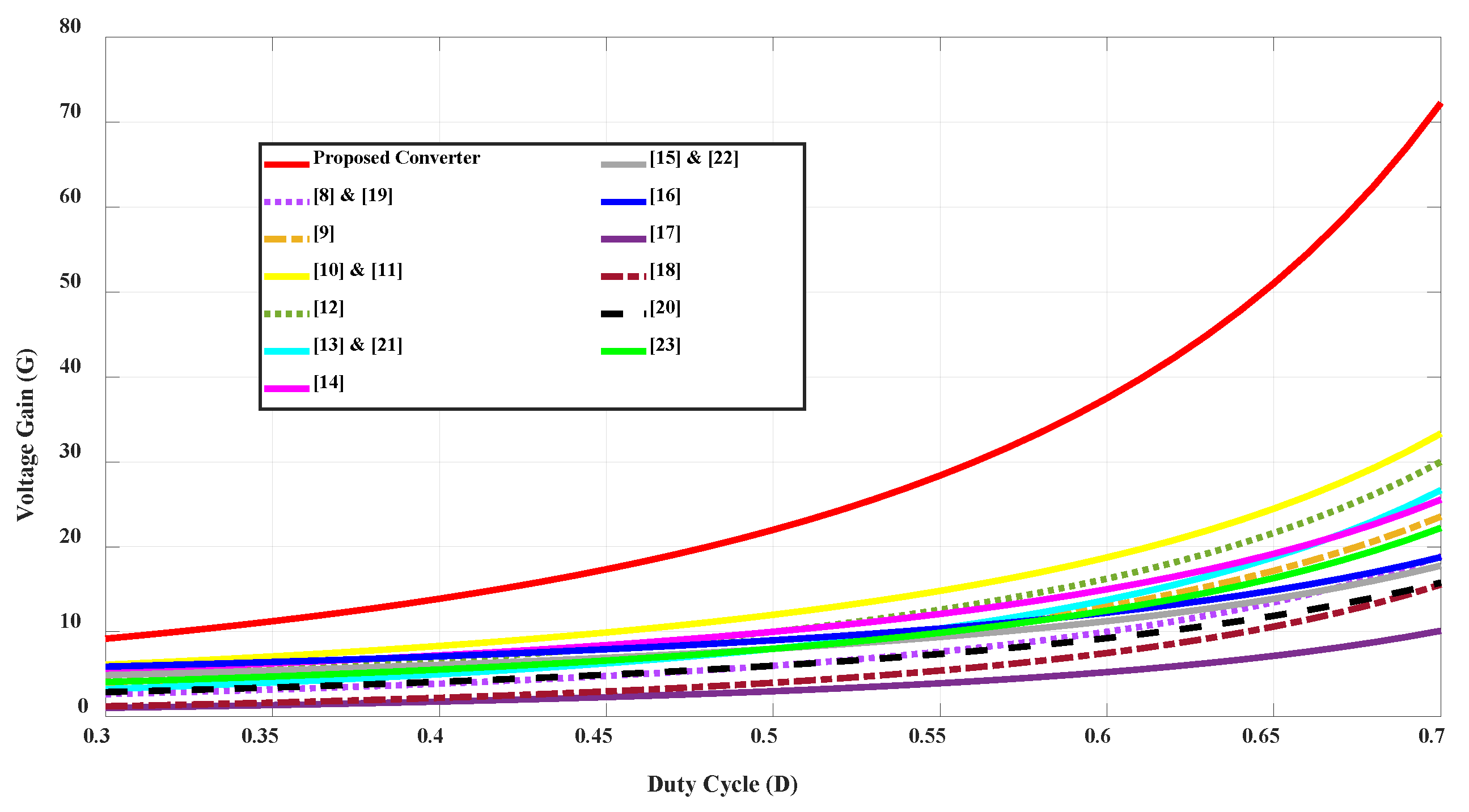
Given that this work focuses on high step-up performance, voltage gain is the primary metric used for evaluation. Using the data from
Table 1,
Figure 14 plots the relationship between gain and duty cycle for all the boost structures reviewed. The results indicate that the proposed configuration provides the highest VG in contrast to the other designs listed in
Table 1.
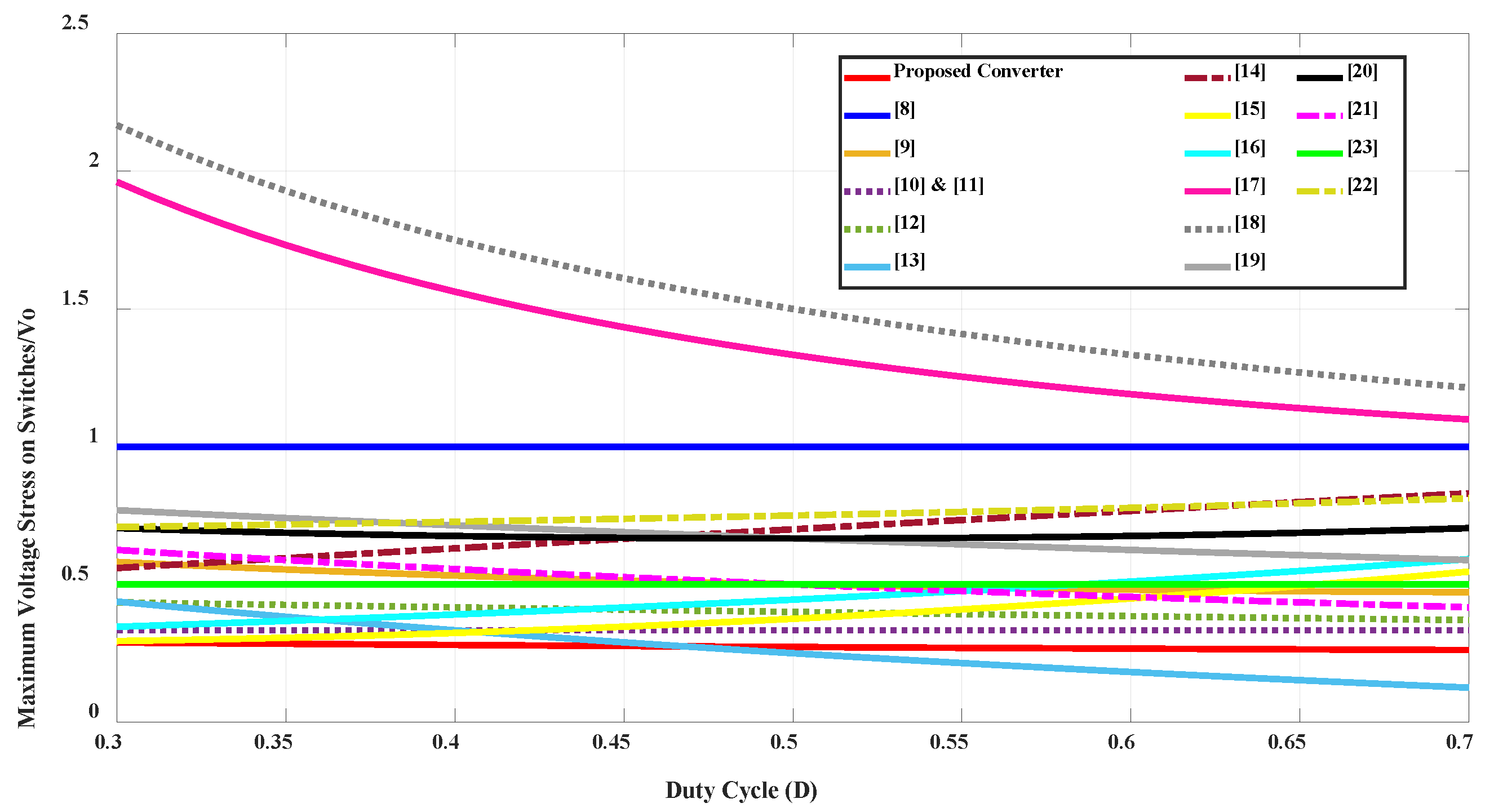
Switch voltage ratings are shown in the second column of
Table 1, with their variation across duty cycles illustrated in
Figure 15. For most operating points, the proposed circuit maintains excellent control over peak switch stress compared to other topologies. The only exception is found in the design from [
13]: above a 50% duty cycle, its maximum switch stress is lower than that of the proposed circuit, but below 50%, the proposed configuration exhibits the lowest stress across all designs. Notably, operating at duty cycles under 50% generally improves converter behavior and reduces losses due to the smaller duty cycle. Another merit of the suggested design is that the switches experience lower voltage levels, allowing for the use of a smaller inductor.
The third column of
Table 1 presents key performance metrics, such as rated power and efficiency. The suggested design is rated for a 400 W output and achieves an efficiency of 95.14%, as verified in
Figure 7. In contrast, most other designs in
Table 1 have ratings below 400 W. Even at the 400 W operating point, the proposed converter maintains 95.14% efficiency, surpassing the efficiency of many competing converters. Several of the compared designs operate at lower power levels but still exhibit lower efficiency than the suggested design.
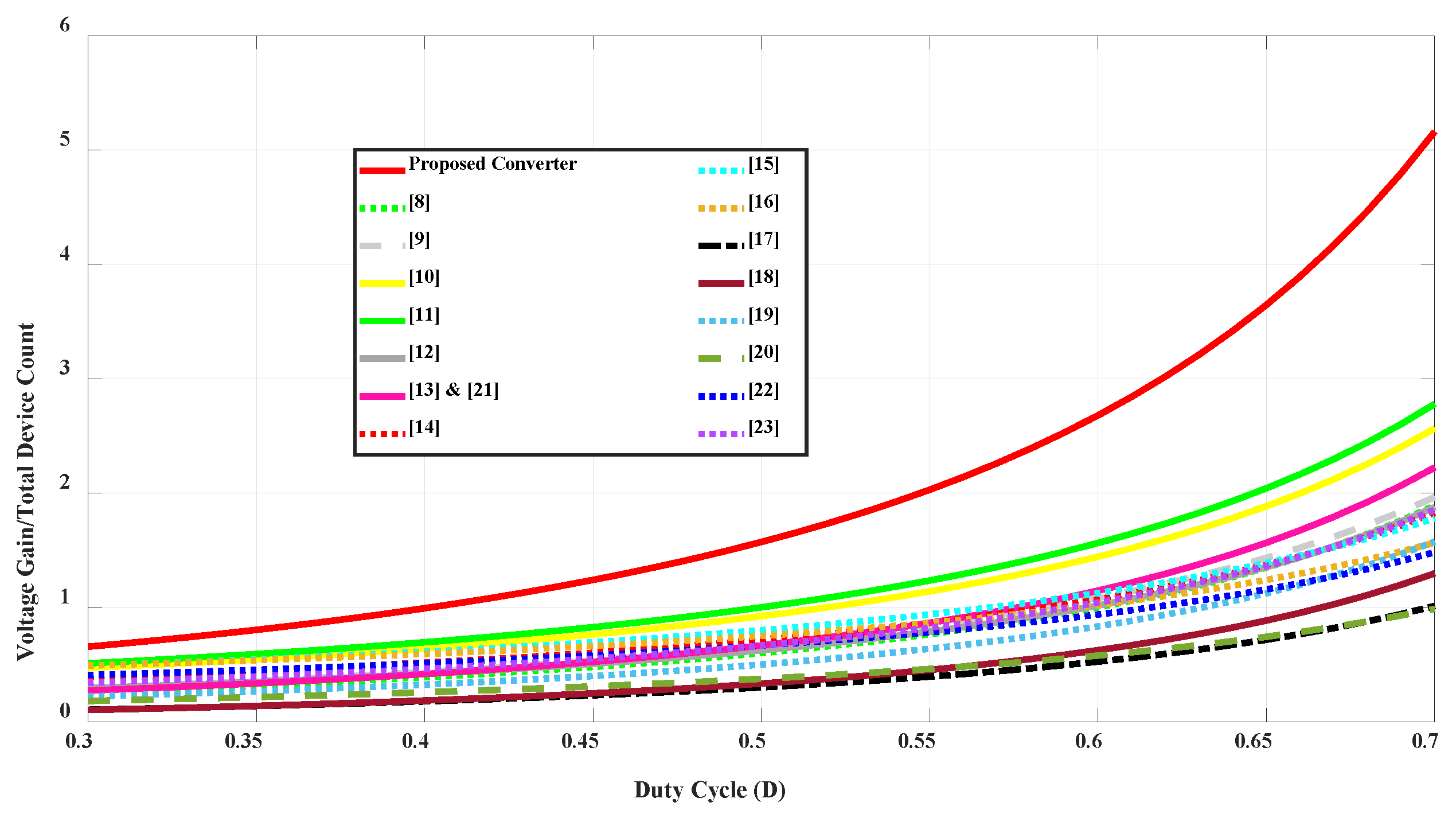
The fourth column reports the component counts, with the final column summarizing the total device count and its breakdown. An ideal design minimizes the number of devices while maximizing voltage gain. To assess this trade-off,
Figure 16 plots voltage gain against the total device count for all configurations. The data shows that the proposed circuit achieves the highest gain per device count, suggesting a cost advantage for similar performance levels. The last part of the comparison evaluates whether a common ground is supported between input and output, which is important as designs without a shared ground tend to be more susceptible to electromagnetic interference, potentially degrading performance. Unlike the designs in [
8,
9,
15,
16,
18], the suggested design supports a common ground.
In conclusion, the comparative analysis highlights the strengths of the proposed converter, including its higher voltage gain, lower switch voltage stress, better gain per device count across duty cycles, and high efficiency at the 400 W level.
7. Experimental Results
To demonstrate the design’s performance and precision, a laboratory prototype rated at 400 W was constructed and implemented for a 19 V input and a 400 V output.
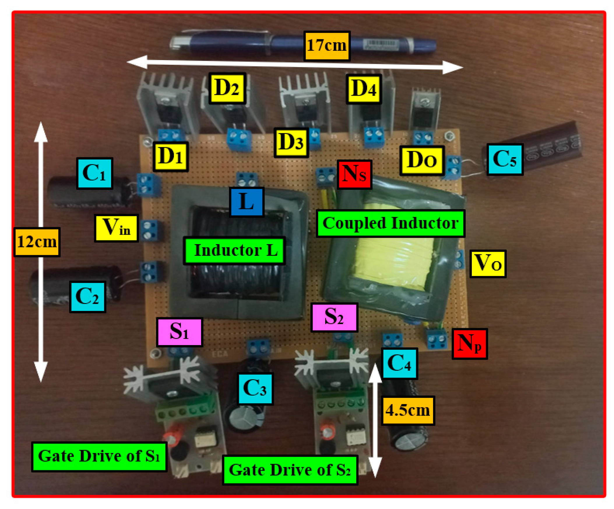
Figure 17 shows images of the experimental prototype. The complete specifications of the prototype are listed in
Table 2. A high-frequency current probe (MICSIG CP2100A, 800 kHz) and a voltage probe were used to capture and analyze the current and voltage waveforms across key components.
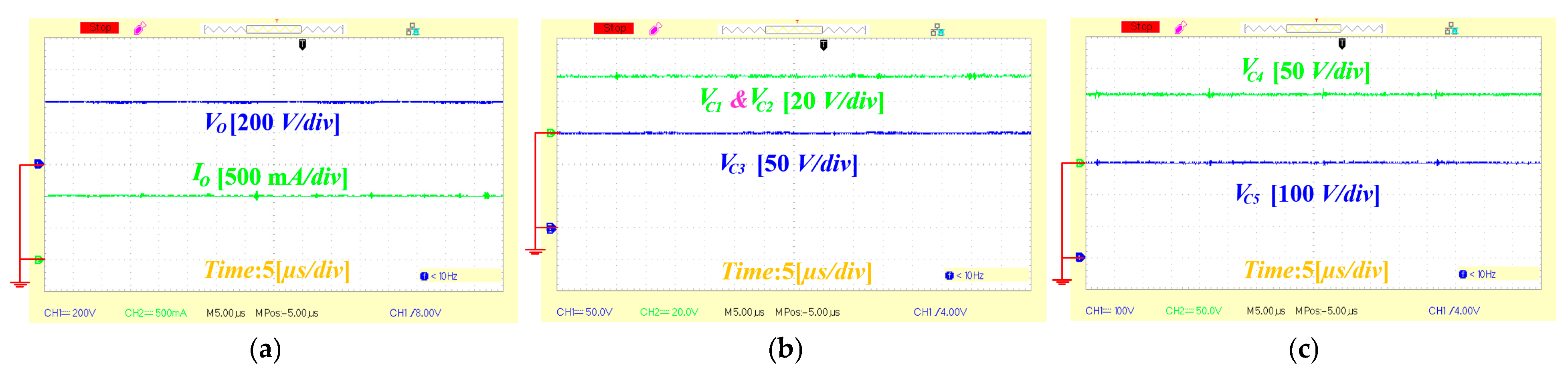
Figure 18a shows an output of 400 V at 1 A. According to Equation (41), the predicted output is 418 V, which is in close agreement with the measured 400 V. Similarly, Equations (36) and (37) estimate 38 V across capacitors C
1 and C
2, and 152 V across C
3. The experimental results show 36 V across C
1 and C
2, and 148 V across C
3, as depicted in
Figure 18b, confirming a strong match with theoretical predictions.
Equations (38) and (39) predict 114 V across C
4 and 304 V across C
5, while the experiments yield 109 V across C
4 and 298 V across C
5, as shown in
Figure 18c, further supporting agreement with theory. In
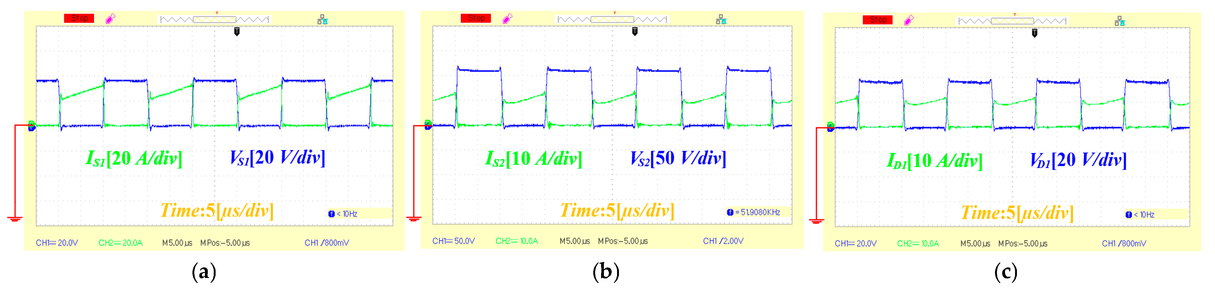
Figure 19a, the waveforms for switch S
1 reveal that, during the first mode, it only experiences a small fraction of the output voltage, around 9%, which aids in minimizing switching losses. The first switching subinterval for the power path through switch S
2 is demonstrated in
Figure 19b. The experimental data from
Figure 19a,b closely match the theoretical results derived from Equations (36), (37), (41), and (42), indicating a strong correlation between the model and experimental findings.
Figure 19c and
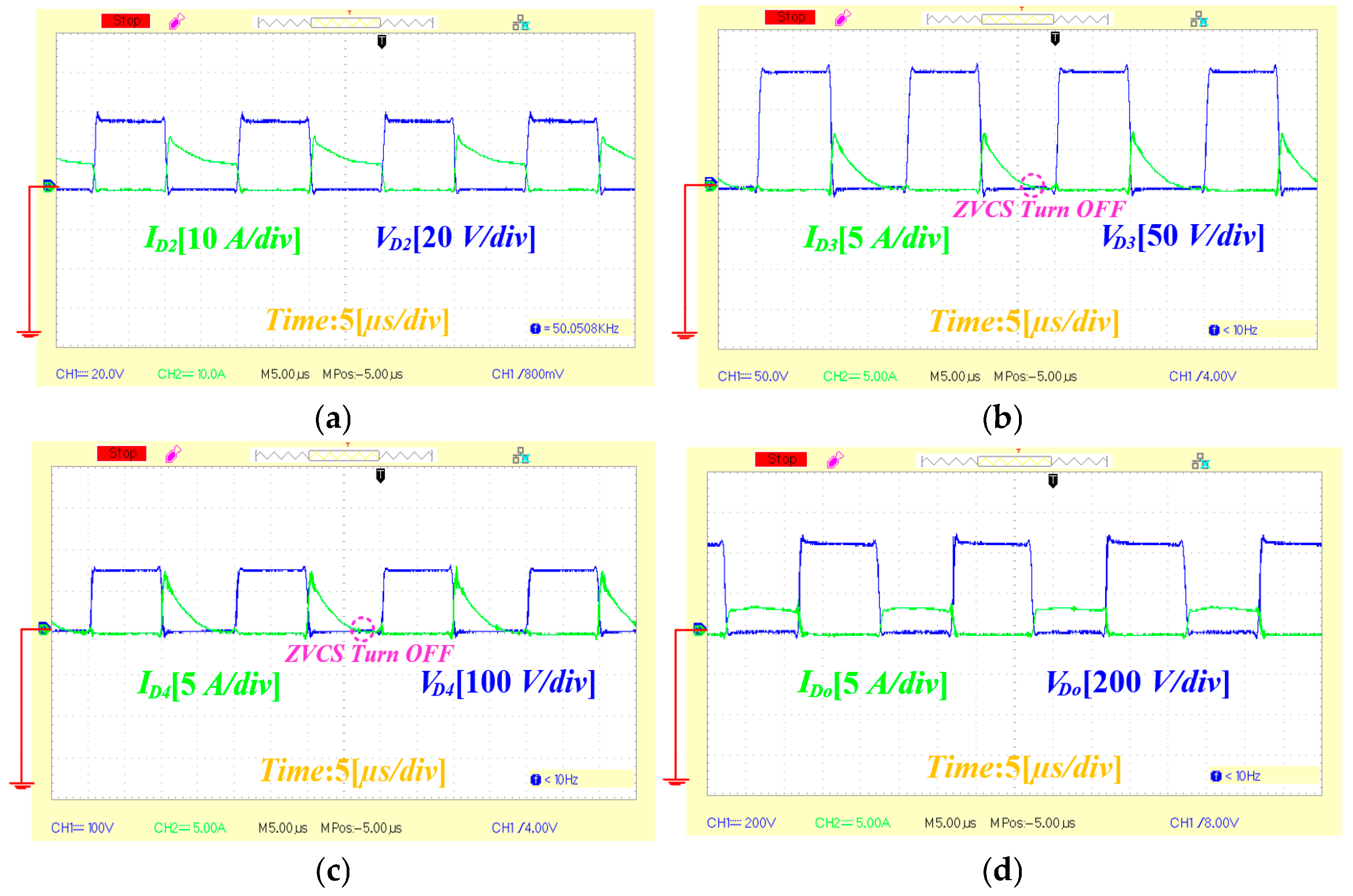
Figure 20a illustrate the voltage and current of diodes D
1 and D
2, with observed values aligning closely with the predictions from Equations (44), (49), and (50).
Additionally, the behaviors of diodes D
3 and D
4, depicted in
Figure 20b,c, where ZVCS occurs during their turn-off, are consistent with theoretical predictions from Equations (45), (51), and (52), confirming a solid agreement between calculated and measured data. The behavior of diode D
O, shown in
Figure 20d, also matches the theoretical expectations from Equations (46) and (51), reinforcing the consistency between the predicted and measured results.





 ,
,