Article

Inter-Arm State-of-Charge Balancing Control Based on Arm Valley Voltage Adjustment in MMDTC-BESS

1
School of Automation and Electronic Engineering, Qingdao University of Science and Technology, Qingdao 266061, China
2
Institute of Electrical Engineering, Chinese Academy of Sciences, Beijing 100190, China
*
Author to whom correspondence should be addressed.
Appl. Sci. 2025, 15(18), 10196; https://doi.org/10.3390/app151810196
Submission received: 8 August 2025 / Revised: 9 September 2025 / Accepted: 16 September 2025 / Published: 18 September 2025

Abstract

This paper addresses a critical challenge in Modular Multilevel DC-link based T-type Converter (MMDTC) battery energy storage systems: the inherent power symmetry between upper and lower arms that prevents natural state-of-charge (SOC) balancing. A novel inter-arm SOC balancing control strategy is proposed that precisely modulates arm valley voltage characteristics—both amplitude and duration—to create controlled power differentials between arms. The theoretical analysis establishes a quantitative relationship between arm valley voltage width and inter-arm power difference, demonstrating that SOC balancing time is inversely proportional to arm valley voltage width. A key advantage of the proposed approach is its adaptive regulation capability: during steady-state operation, closed-loop feedback maintains arm valley voltage width within a narrow range through real-time SOC differential assessment, ensuring dynamic SOC equilibrium while minimizing impact on output power quality. The strategy works effectively in both charging and discharging modes, with comprehensive control logic for various operational scenarios. Finally, simulation and experimental results confirmed the effectiveness of the proposed control strategy.

1. Introduction

The global energy landscape is undergoing a profound transformation toward sustainability, with renewable energy installations experiencing unprecedented growth. In 2024, renewable sources accounted for over 80% of newly added global power generation capacity [1,2]. However, the inherent variability and intermittency of renewable energy sources present significant challenges to grid stability, manifesting as frequency fluctuations and voltage deviations [3,4]. Battery energy storage systems (BESS) have emerged as a pivotal solution to address these challenges, offering rapid power regulation, bidirectional energy flow, and high conversion efficiency [5,6]. Among various energy storage technologies, BESS stands out as particularly promising due to its mature technology, declining costs, and superior dynamic response characteristics [7,8].
The power conversion system (PCS) serves as the critical interface between battery arrays and the power grid, with its topology directly determining system performance, efficiency, and reliability [9]. As the BESS industry matures, there has been a notable evolution from conventional two- and three-level converter topologies toward advanced multilevel configurations.
Conventional two- and three-level converters face fundamental limitations in high-power applications. The voltage stress on semiconductor devices and constraints in battery pack configurations typically restrict single-unit capacity to approximately 500 kW. Furthermore, integration with medium- and high-voltage grids necessitates bulky line-frequency transformers, significantly increasing system cost and footprint [10,11]. In contrast, multilevel topologies such as Cascaded H-Bridge (CHB) and Modular Multilevel Converter (MMC), as shown in Figure 1a,b, offer transformative advantages through their modular architecture. These topologies enable direct grid connection at medium and high voltages without step-up transformers, while their distributed structure facilitates the segmentation of large battery arrays into independently manageable units—a critical requirement for safety and reliability in utility-scale BESS [12,13,14].
The Modular Multilevel DC-link based T-type Converter (MMDTC) represents an innovative topology that synergistically combines the advantages of both CHB and MMC [15,16]. As shown in Figure 1c, this topology features a unique configuration where a T-type converter interfaces with a modular multilevel DC-link, achieving superior performance with reduced semiconductor count and enhanced efficiency. Despite these advantages, the MMDTC faces a critical operational challenge common to all multilevel BESS: state-of-charge (SOC) balancing control. SOC imbalances not only accelerate battery degradation and reduce system efficiency but also compromise power quality and operational reliability. Research indicates that effective SOC management can extend battery lifetime by up to 30% while maintaining optimal system performance [17,18].
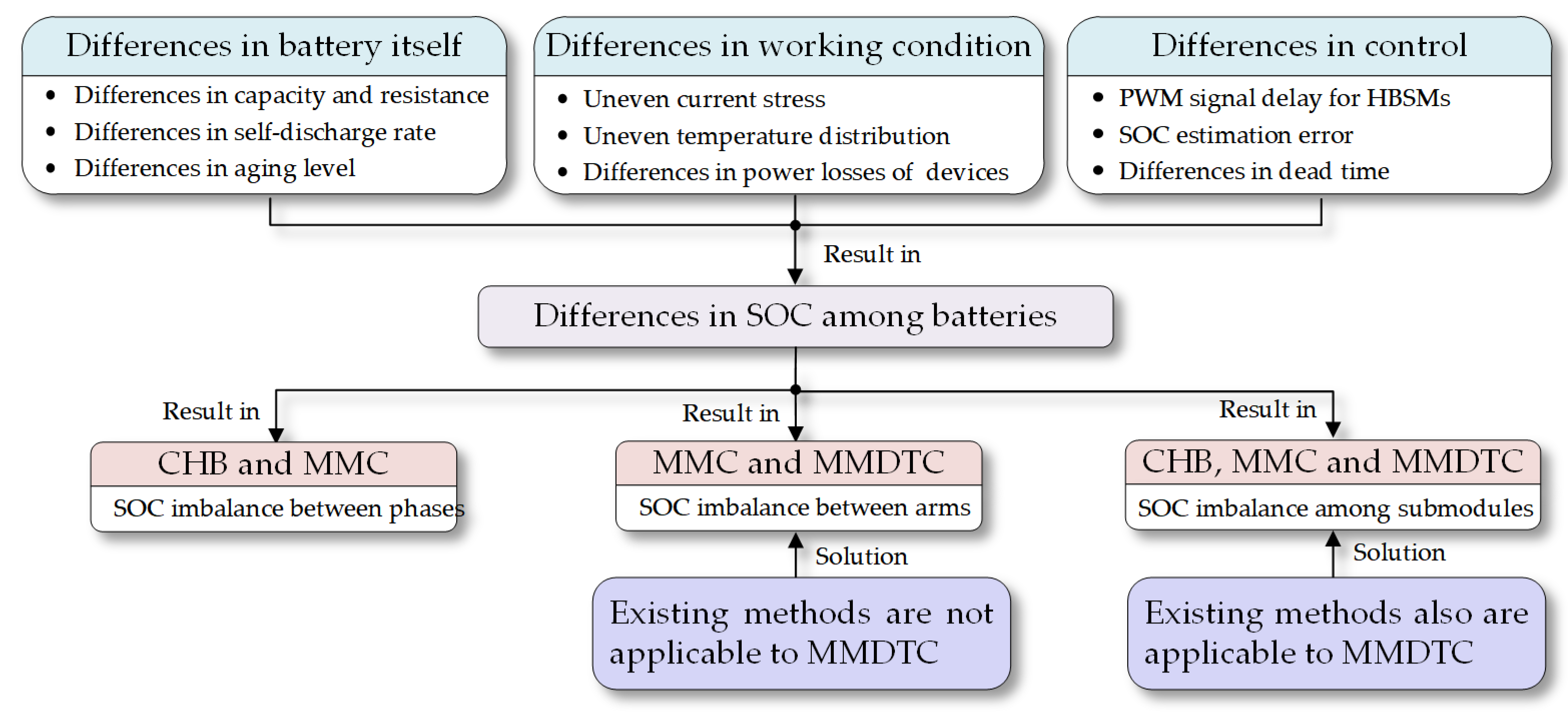
The SOC imbalance phenomenon in multilevel BESS exhibits hierarchical complexity, as illustrated in Figure 2. At the fundamental level, battery cell-to-cell variations arise from manufacturing tolerances, working condition, and control condition [19,20]. These microscopic imbalances propagate through the system hierarchy, manifesting as phase-level, arm-level, and submodule-level disparities. The specific imbalance patterns are topology-dependent: CHB systems primarily experience inter-phase and inter-submodule imbalances; MMC systems exhibit three-dimensional imbalances across phases, arms, and submodules; while MMDTC, due to its three-phase common DC-link configuration, predominantly faces inter-arm and inter-submodule imbalances.
Existing literature provides well-established solutions for submodule-level SOC balancing through modulation refinement and sorting algorithms, successfully demonstrated in both CHB and MMC applications [21,22,23,24]. These methods remain theoretically applicable to MMDTC systems. However, inter-arm SOC balancing presents unique challenges that existing solutions cannot adequately address.
In MMC systems, inter-arm balance is typically achieved through circulating current injection, DC bias adjustment, or power redistribution strategies [25,26,27]. However, these approaches fundamentally rely on multi-phase circulating current paths that are absent in the MMDTC’s single arm-pair configuration. Similarly, CHB systems employ zero-sequence voltage or negative-sequence current injection for inter-phase balancing [28,29,30], but the MMDTC’s line voltage output configuration inherently suppresses zero-sequence components, rendering these methods ineffective.
This fundamental incompatibility between existing balancing strategies and the MMDTC topology creates a critical research gap. The unique structural characteristics of MMDTC—combining a three-phase common DC-link with a T-type output stage—necessitate the development of novel control strategies specifically tailored to its architecture. Therefore, this paper addresses this gap by proposing an innovative inter-arm SOC balancing strategy based on arm valley voltage adjustment, providing both theoretical foundation and practical implementation for MMDTC-BESS applications.
The remainder of this paper is organized as follows: Section 2 presents a detailed description of the MMDTC-BESS topology and operating principles, analyzing the inherent power balance characteristics between arms and their impact on SOC balancing. Section 3 proposes the inter-arm SOC balancing control strategy based on arm valley voltage adjustment, establishes the quantitative relationship model between arm valley voltage width and inter-arm power difference, and analyzes the impact of this strategy on output waveform quality. Section 4 presents the simulation and experimental results. Finally, Section 5 summarizes the main contributions and conclusions of this research.

2. MMDTC-BESS Topology and Operating Principles

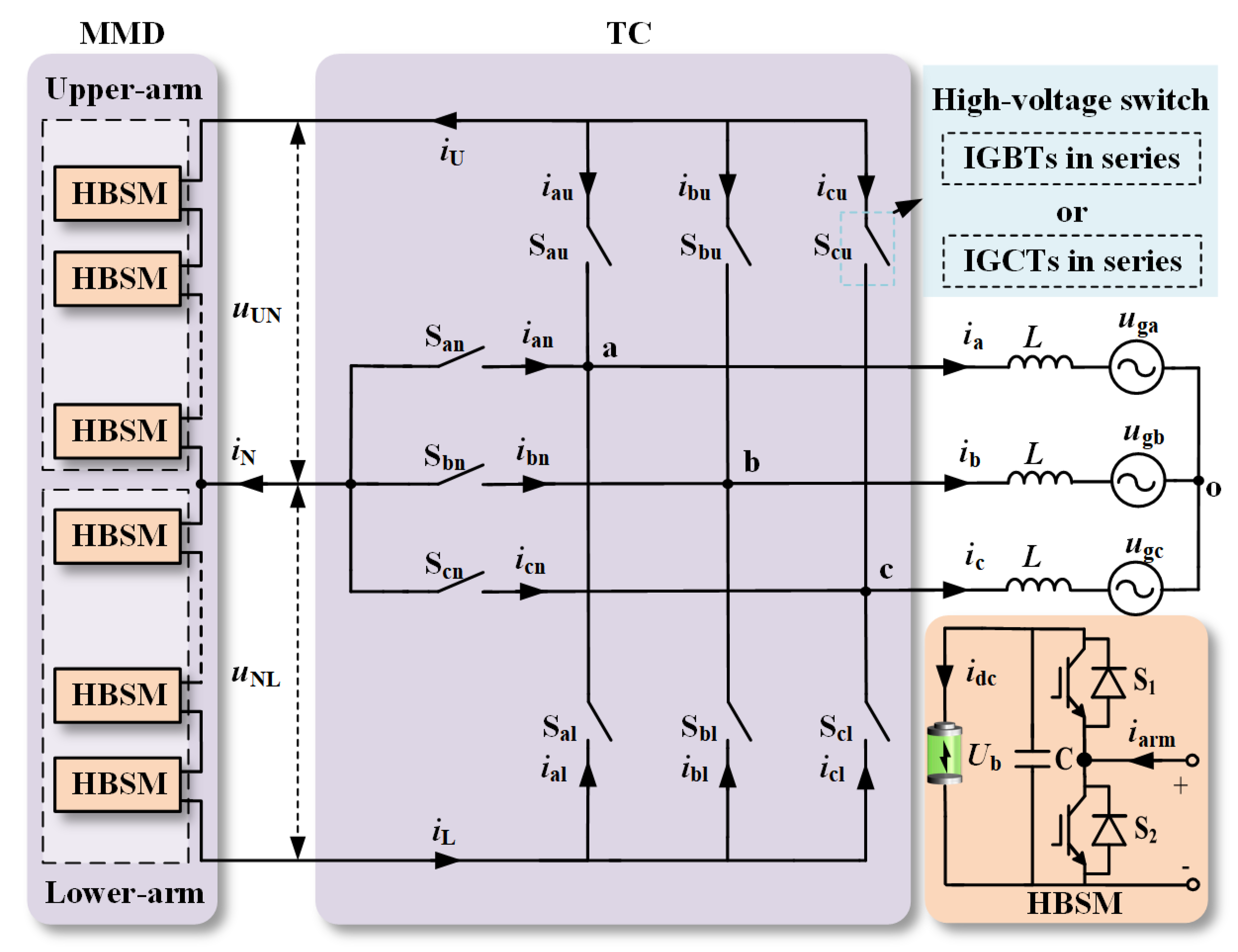
Figure 3 illustrates the topology of the MMDTC-BESS, which consists of a modular multilevel DC-link and a T-type structure. The DC-link comprises both upper and lower arms, with each arm constructed by cascading N half-bridge submodules and integrating battery units within these submodules. The T-type structure employs four high voltage switches per phase, formed by series-connected IGBTs or IGCTs. The DC side of the T-type structure is connected to the modular multilevel DC-link, collectively forming the complete MMDTC-BESS.
The output phase voltages of the MMDTC-BESS are defined as follows:
u ao = V sin ( ω t + π 6 ) u bo = V sin ( ω t π 2 ) u co = V sin ( ω t + 5 π 6 )
where V and ω are the amplitude of the phase voltage and the angular frequency, respectively.
Moreover, the expression for the output line voltages of the MMDTC-BESS can be derived as follows:
u ab = 3 V sin ( ω t + π 3 ) u bc = 3 V sin ( ω t π 3 ) u ca = 3 V sin ( ω t + π )
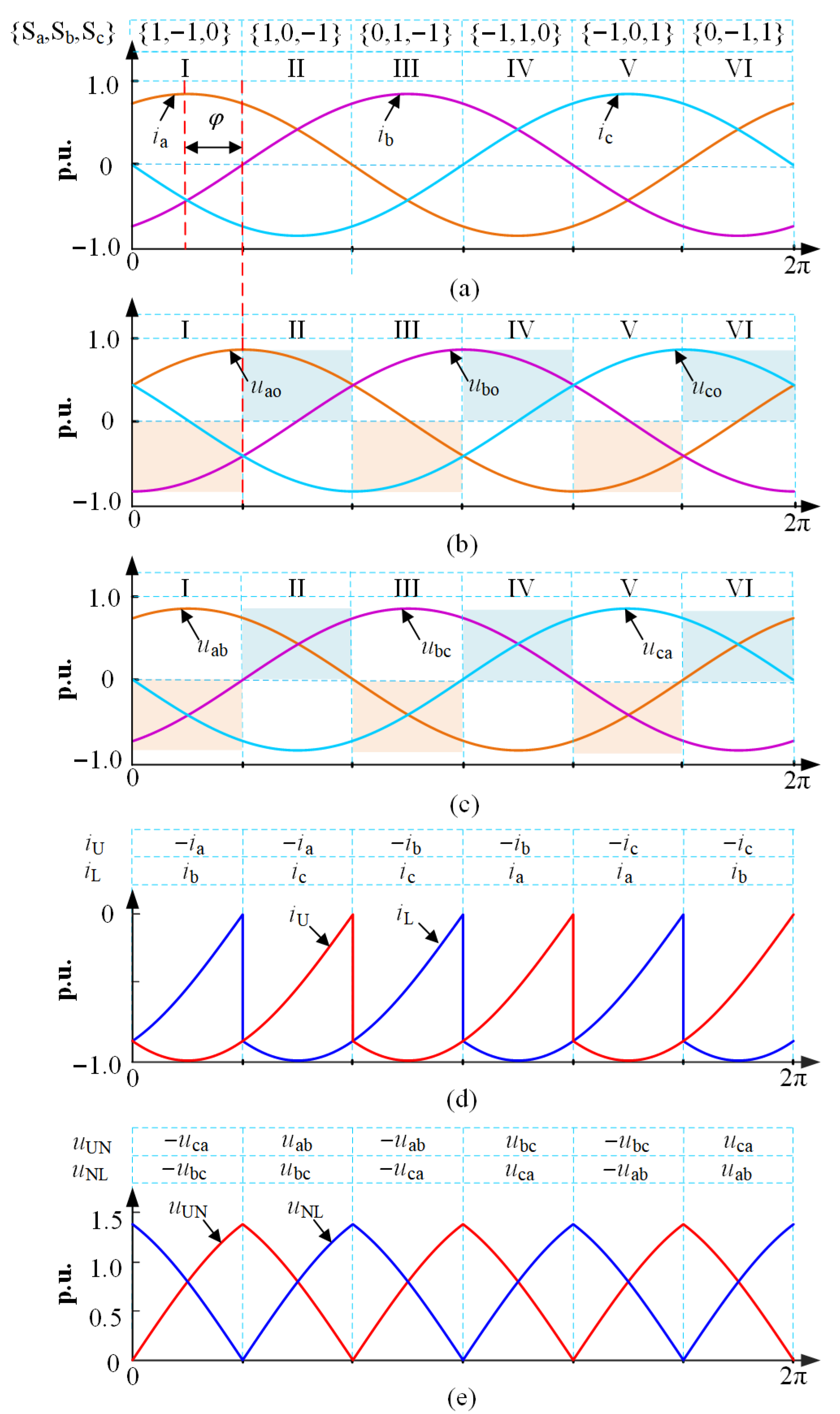
The relationship between the upper and lower arm voltages and the line voltages is depicted in Figure 4. Each phase of the T-type structure contains three switches: Sku, Skn, and Skl (where k = a, b, c). At any given moment for each phase, only one switch is in the ON state while the other two remain in the OFF state. Taking phase A as an example, the switching state Sa is a function of {Sau, San, Sal}: when {Sau, San, Sal} = {1, 0, 0}, Sa = 1; when {Sau, San, Sal} = {0, 1, 0}, Sa = 0; when {Sau, San, Sal} = {0, 0, 1}, Sa = −1. Furthermore, {Sa, Sb, Sc} represents the switching states of the three phases in the T-type structure. Based on these switching states, mathematical expressions for the arm voltages can be derived as follows:
u UN = 3 V sin θ , θ [ 0 , π 3 ) 3 V sin ( θ + π 3 ) , θ [ π 3 , 2 π 3 ]
u NL = 3 V sin ( θ π 3 ) ,   θ [ 0 , π 3 ) 3 V sin ( θ π 3 ) , θ [ π 3 , 2 π 3 ]
where θ = ω t 2 π 3 f l o o r ω t / 2 π 3 , floor (x) represents the floor function.
The three-phase currents of the MMDTC-BESS are defined as follows:
i a = I sin ( ω t + π 6 ) i b = I sin ( ω t π 2 ) i c = I sin ( ω t + 5 π 6 )
where I and φ represent the current amplitude and the power factor angle, respectively.
Based on the switching state combinations of the T-type structure depicted in Figure 4, the arm current expressions can be derived as follows:
i U = I sin ( θ + π 6 + φ ) ,   θ [ 0 , 2 π 3 ]
i L = I sin ( θ π 2 + φ ) , θ [ 0 , π 3 ) I sin ( θ + 5 π 6 + φ ) , θ [ π 3 , 2 π 3 ]
The arm instantaneous power can be calculated based on Equations (3), (4), (6) and (7), as expressed below:
p UN = 3 V I sin θ sin ( θ π 6 + φ ) , θ [ 0 , π 3 ) 3 V I sin ( θ + π 3 ) sin ( θ π 6 + φ ) , θ [ π 3 , 2 π 3 ]
p NL = 3 V I sin ( θ π 3 ) sin ( θ π 2 + φ ) , θ [ 0 , π 3 ) 3 V I sin ( θ π 3 ) sin ( θ + 5 π 6 + φ ) , θ [ π 3 , 2 π 3 ]
Furthermore, the arm average power can be calculated using the following expressions:
p UN = 3 2 π 0 2 π / 3 u UN i U d ( ω t ) = 3 4 V I cos ( φ )   p UN = 3 2 π 0 2 π / 3 u NL i L d ( ω t ) = 3 4 V I cos ( φ )
As indicated by Equation (10), under normal operating conditions, the upper and lower arms maintain identical average power, resulting in an inherent power balance that prevents natural SOC equalization. Since SOC regulation fundamentally depends on controlling the average power flow through each arm, this intrinsic power symmetry poses a critical challenge: when SOC imbalances develop between arms, the system lacks an inherent mechanism to restore equilibrium. The equal power distribution, while ensuring stable operation, paradoxically prevents the differential power flow necessary for SOC correction. To address this fundamental limitation, this paper proposes a dedicated inter-arm SOC balancing control strategy that deliberately breaks the power symmetry by introducing controlled power differentials between arms, thereby enabling active SOC equalization while maintaining system stability.

3. Proposed Inter-Arm SOC Balance Control Strategy

3.1. The Adjustment of Arm Valley Voltage

According to Equation (10), inter-arm power differential can theoretically be achieved through either voltage or current modulation. However, current-based regulation presents significant practical challenges. As illustrated in Figure 4, modulating inter-arm current distribution requires dynamic alteration of the T-type converter’s switching state combinations {Sa, Sb, Sc}, which introduces two fundamental limitations. First, the high-voltage switching devices commonly used in T-type converters typically operate at low switching frequencies; frequent switching transitions may degrade system reliability and efficiency. Second, changes in switching states directly influence the converter’s output voltage, resulting in variations in the output current. This strong voltage-current coupling significantly complicates the control system design and hinders precise power regulation.
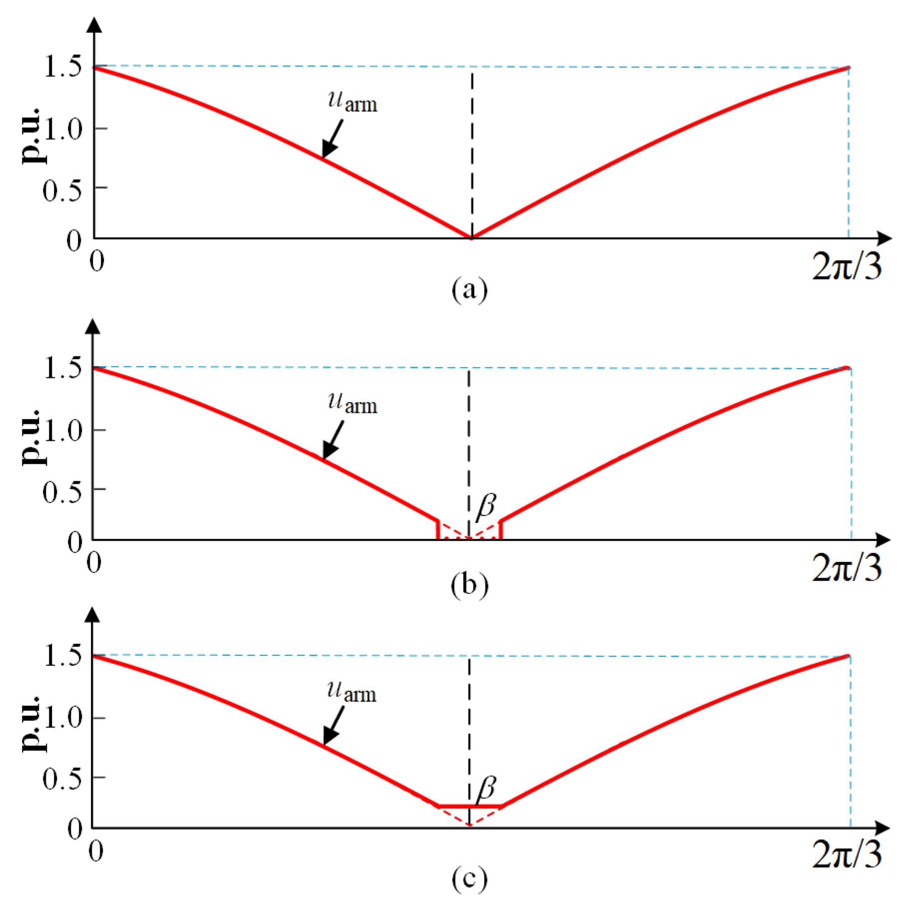
Given these constraints, a more sophisticated approach involves modulating the arm voltage directly. The modular architecture of MMDTC, comprising multiple series-connected submodules per arm, provides exceptional flexibility for voltage waveform shaping. A distinctive characteristic of the arm voltage waveform, highlighted in Figure 5a, is the presence of valley regions that correspond to zero-voltage intervals. By precisely controlling both the amplitude and duration of these valley voltages, the arm’s time-averaged voltage—and consequently its power flow—can be effectively regulated without disrupting the fundamental T-type switching pattern.
Two complementary adjustment strategies have been developed:
(1) Duration Extension of Arm Valley Voltage (Figure 5b): The arm average voltage is reduced by extending the zero-voltage interval from its nominal value to a controlled duration β. This technique effectively increases the proportion of time during which the arm operates at zero voltage, thereby decreasing the time-averaged voltage through duty cycle modification.
(2) Both Amplitude and Duration Increase in Arm Valley Voltage (Figure 5c): The arm average voltage is increased through a dual-parameter approach that simultaneously elevates the arm valley voltage amplitude from zero to a predetermined positive value while extending its duration. This combined adjustment mechanism provides enhanced control flexibility, enabling fine-grained power regulation with improved dynamic response characteristics.
The proposed arm valley voltage adjustment strategy fully exploits the inherent structural advantages of modular multilevel converters, enabling precise power control through targeted modulation of local voltage waveform characteristics. By leveraging the flexibility afforded by the modular architecture, differential power distribution between arms can be achieved without compromising system stability or efficiency.
The fundamental objective of arm voltage adjustment is to establish precise control over inter-arm power flow. To address diverse operational requirements, four comprehensive power regulation strategies have been systematically developed, each tailored to specific battery charging-discharging states and SOC balancing requirements:
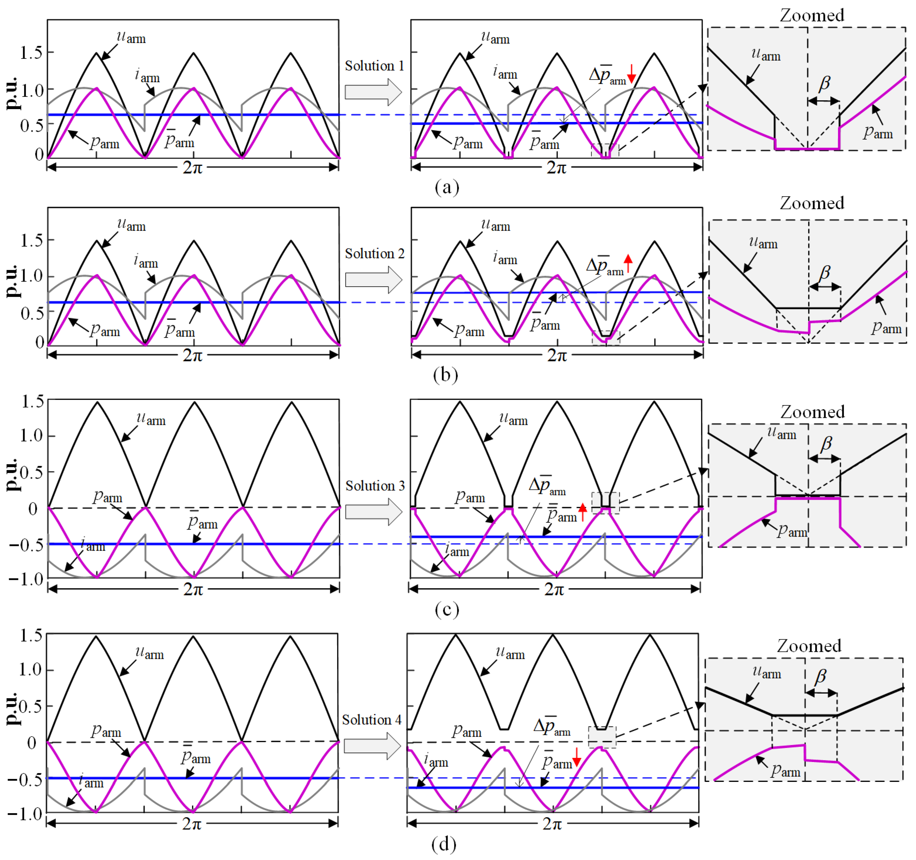
(1) Solution 1—Charging Power Reduction: As illustrated in Figure 6a, charging power is effectively reduced by extending the zero-voltage interval duration. This extension increases the duty cycle of the low-voltage state, thereby limiting energy absorption during the charging process while maintaining stable operation.
(2) Solution 2—Charging Power Enhancement: Figure 6b demonstrates power augmentation through simultaneous elevation of arm valley voltage amplitude and extension of its duration. This dual-parameter approach optimizes the voltage waveform to maximize energy absorption capacity during charging operations.
(3) Solution 3—Discharging Power Reduction: Power output is moderated by prolonging the zero-voltage duration, as shown in Figure 6c. The increased low-level duty cycle effectively constrains the energy release rate, enabling controlled discharging when power limitation is required.
(4) Solution 4—Discharging Power Enhancement: Figure 6d illustrates power amplification through combined arm valley voltage elevation and duration extension. This approach maximizes power delivery capability by optimizing the voltage waveform characteristics during discharging operations.
The practical implementation of inter-arm SOC balancing requires coordinated deployment of these four solutions based on real-time SOC differential assessment. Table 1 presents the comprehensive control logic for various operational scenarios:
(1) During Charging Operations:
When SOCUN > SOCNL: Solution 1 is applied to the upper arm to restrict its charging rate, while Solution 2 is simultaneously implemented on the lower arm to accelerate its charging. This “suppress-high, enhance-low” approach effectively equalizes the SOC levels by differentially controlling the charging rates.
When SOCUN < SOCNL: The control logic is reversed—Solution 2 enhances upper arm charging while Solution 1 limits lower arm charging, thereby achieving complementary SOC adjustment.
(2) During Discharging Operations:
The same differential control philosophy is applied using Solution 3 and 4. The high-SOC arm undergoes accelerated discharging through Solution 4, while the low-SOC arm experiences moderated discharging via Solution 3, progressively converging the SOC levels toward equilibrium.
This systematic approach ensures robust SOC balancing across all operational modes while maintaining optimal power flow control.
When during the charging operation and SOCUN > SOCNL, the refined arm voltage is derived by implementing the control strategy outlined in Table 1:
u UN _ ad = 3 V sin θ , θ [ β , π 3 ) 3 V sin ( θ + π 3 ) , θ ( π 3 , 2 π 3 β ] 0 , θ [ 0 , β ) ( 2 π 3 β , 2 π 3 ]
u NL _ ad = 3 V sin ( θ π 3 ) , θ [ 0 , π 3 β ) 3 V sin ( β ) , θ [ π 3 β , π 3 + β ] 3 V sin ( θ π 3 ) ,   θ ( π 3 + β , 2 π 3 ]
Assuming that the arm current remains constant during the process of voltage fine-tuning, the arm instantaneous power expressions can be derived from Equations (6), (7), (11) and (12) as follows:
p UN _ ad = 3 V I sin θ sin ( θ π 6 + φ ) , θ [ β , π 3 ) 3 V I sin ( θ + π 3 ) sin ( θ π 6 + φ ) , θ ( π 3 , 2 π 3 β ] 0 , θ [ 0 , β ) ( 2 π 3 β , 2 π 3 ]
p NL _ ad = 3 V I sin ( θ π 3 ) sin ( θ π 2 + φ ) , θ [ 0 , π 3 β ) 3 V I sin ( β ) sin ( θ π 2 + φ ) , θ [ π 3 β , π 3 ) 3 V I sin ( β ) sin ( θ + 5 π 6 + φ ) , θ [ π 3 , π 3 + β ) 3 V I sin ( θ π 3 ) sin ( θ + 5 π 6 + φ ) , θ ( π 3 + β , 2 π 3 ]
Furthermore, the expressions for arm average power can be derived as follows:
p ¯ UN _ ad = 3 V I 6 β + 3 sin 2 β + 3 cos 2 β 3 + 2 π 8 π cos φ
p NL _ ad = 3 V I 6 β + 12 sin β 3 sin 2 β 3 cos 2 β + 3 + 2 π 8 π cos φ
Based on Equations (15) and (16), the inter-arm power difference can be derived as follows:
| Δ p | = | p ¯ UN _ ad p ¯ NL _ ad | = 3 V I sin β 3 sin β 3 cos β + 3 2 π cos φ
Similarly, the inter-arm power difference under the other three operating conditions listed in Table 1 can be derived, as demonstrated by Equation (17).
The inter-arm average power difference | p | , along with its ratio to the arm average power, can be determined using Equations (17) and (10):
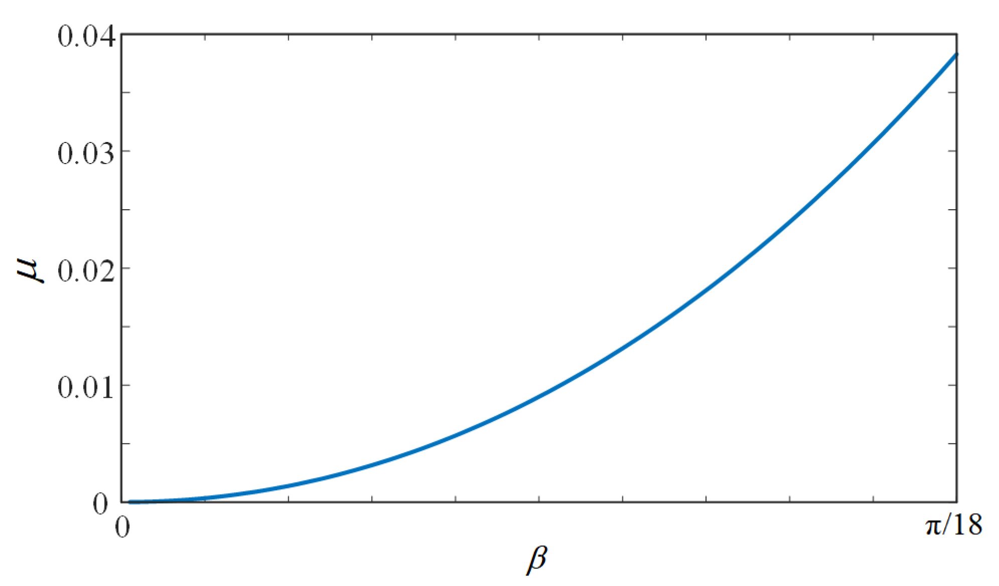
μ = p p ¯ UN = 2 sin β 3 sin β 3 cos β + 3 π
As illustrated in Equation (18), the ratio μ is expressed as a function of β , with the corresponding functional curve depicted in Figure 7. μ exhibits a positive correlation with β , and a maximum power regulation capability of approximately 4% can be achieved when condition β < π / 18 is met.
For the purpose of analysis, the distinctions between submodules within the arm are considered negligible, with each submodule assumed to possess equal charging and discharging power. Based on the principle of power conservation, the following equation is derived:
N U b i dc = p ¯ arm
where U b and idc signifies the battery voltage and average current entering the battery, respectively.
The submodule SOC is derived using the ampere-hour integration method, as outlined below:
SOC SM = SOC SM ( t 0 ) + 1 C rate t 0 t i dc d ( t )
where C r a t e represents the rated capacity of the submodule battery.
From Equations (19) and (20), it can be concluded that:
N SOC SM = N SOC SM ( t 0 ) + p _ arm U b C rate ( t t 0 )
Definition SOC arm = N SOC SM , the aforementioned equation can be rewritten as:
SOC arm = SOC arm ( t 0 ) + p _ arm U b C rate ( t t 0 )
According to Equation (22), the inter-arm SOC difference can be derived as follows:
SOC = SOC UN SOC NL = SOC UN ( t 0 ) SOC NL ( t 0 ) + p ¯ UN _ ad p ¯ NL _ ad U b C rate ( t t 0 )
The time required for the inter-arm SOC to attain an equilibrium state ( SOC = 0 ) can be determined as t by integrating Equations (17) and (23):
t = t t 0 = 2 π U b C rate SOC ( t 0 ) 3 V I sin β 3 sin β 3 cos β + 3
where SOC ( t 0 ) represents the inter-arm initial SOC difference.
In a similar manner, the same relational expression can be derived by examining the other three cases.
Equation (24) establishes a precise mathematical relationship among Δt, β, and ΔSOC. In practical implementations, the balance time Δt can be flexibly configured according to specific system requirements and operational constraints. Once Δt is predetermined and ΔSOC is measured, the required β value can be directly calculated using Equation (24), enabling real-time adaptive control.
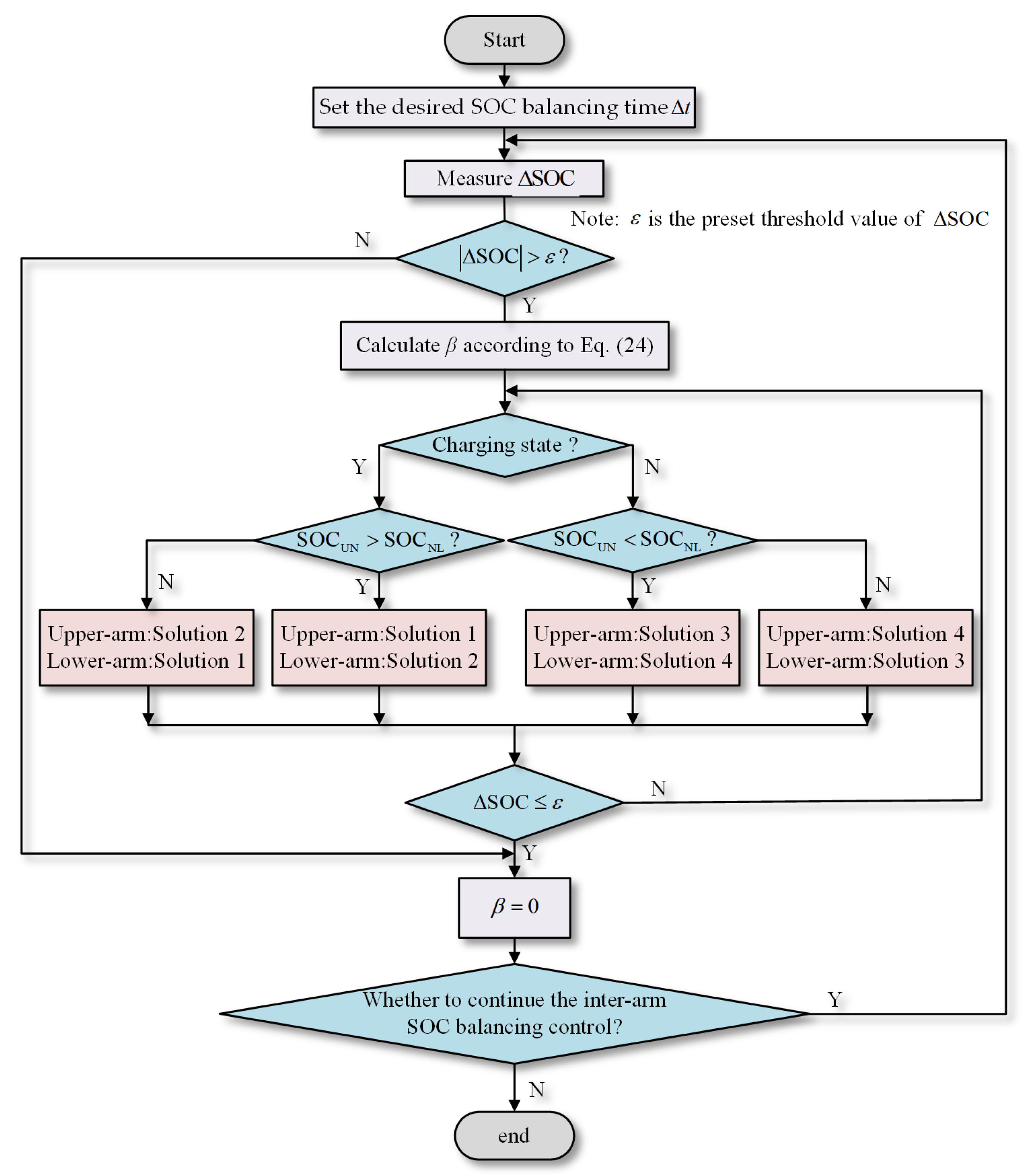
Based on this mathematical framework, a comprehensive inter-arm SOC balancing control algorithm has been developed, as illustrated in Figure 8. The implementation follows a systematic five-step procedure:
Step 1: The desired SOC equilibrium time Δt is determined based on operational requirements, battery characteristics, and system performance specifications. This parameter defines the convergence rate of the SOC balancing process.
Step 2: The battery management system continuously monitors and calculates the ΔSOC, providing real-time feedback for the control algorithm.
Step 3: The measured ΔSOC is substituted into Equation (24) to compute the corresponding β.
Step 4: Based on the battery’s operational mode (charging/discharging) and the polarity of ΔSOC, the appropriate arm voltage adjustment strategy is selected from the predefined control matrix presented in Table 1. This ensures optimal power flow direction for SOC convergence.
Step 5: The algorithm continuously evaluates whether |ΔSOC(t)| has fallen below the predetermined threshold ε. If |ΔSOC(t)| > ε, the SOC balancing control continues. Once |ΔSOC(t)| ≤ ε is satisfied, indicating successful SOC equilibrium, the modulation parameter is reset (β = 0) and normal operation resumes.
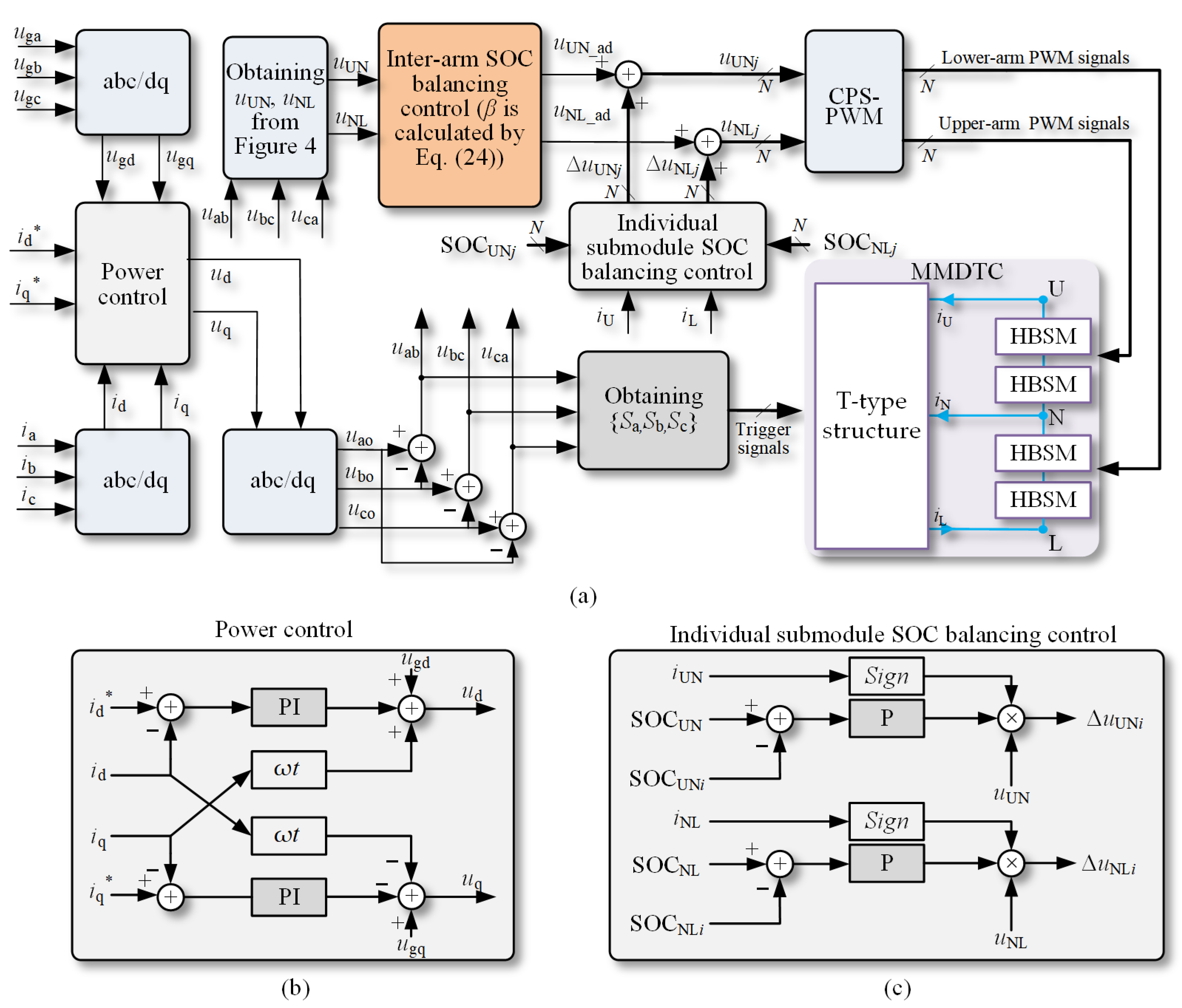
Figure 9a illustrates the comprehensive control architecture of the MMDTC-BESS system. The β parameter, calculated using Equation (24), serves as a key control variable and is seamlessly integrated into the existing control framework. The modulation wave is generated by the internal power control loop of the system. Based on the structure shown in Figure 4, the control signals for the T-type structure and the modulation waves for the upper and lower arms of the DC link can be further derived. Finally, carrier phase-shifted pulse width modulation (CPS-PWM) is adopted as the core modulation strategy for the converter, while incorporating mature technologies such as power control with Proportional-Integral (PI) controllers and submodule-level SOC balancing control with P controllers as shown in Figure 9b,c, respectively. Given that these conventional control methods have been thoroughly elaborated in the existing literature, this paper does not discuss their specific implementation details in depth.

3.2. The Impact of Arm Voltage Valley Adjustment on Output Waveform Quality

This section provides a comprehensive analysis of how arm valley voltage adjustment affects the output voltage waveform quality in MMDTC. Under normal operation, the MMDTC synthesizes high-quality sinusoidal output voltages through precise superposition of upper and lower arm voltages. However, the implementation of inter-arm SOC balancing control necessitates deliberate modifications to the conventional voltage synthesis pattern, which inevitably influences the harmonic performance of the three-phase output. Figure 10 illustrates these effects through comparative waveform analysis, clearly demonstrating the spectral changes induced by arm valley voltage modulation.
Figure 11 presents a detailed quantitative assessment of the relationship between the β and output voltage total harmonic distortion (THD). As evident from Figure 11a, the THD exhibits a monotonically increasing relationship with β, indicating progressive waveform degradation as the β increases.
The spectral decomposition presented in Figure 11b reveals the underlying mechanism: the THD elevation is predominantly caused by the emergence of even-order harmonics, particularly the 2nd and 4th components. This phenomenon directly results from the asymmetrical voltage modulation introduced between the upper and lower arms, which disrupts the natural harmonic cancelation inherent in balanced MMDTC operation.
These findings reveal a fundamental trade-off in the proposed control strategy: while larger β values accelerate inter-arm SOC convergence, they simultaneously compromise output power quality. This necessitates a holistic optimization approach that balances SOC equilibrium requirements against THD.
A particularly advantageous feature of the proposed strategy is its inherent adaptive regulation capability. As demonstrated in Figure 6, continuous application of the control algorithm drives ΔSOC toward zero, where it stabilizes with only minor fluctuations within the predetermined threshold ε. This convergence behavior has significant practical implications: as ΔSOC approaches zero, the required β value diminishes correspondingly, automatically reducing the harmonic impact on output waveforms.

4. Simulation and Experimental Verification

4.1. Simulation Verification

To verify the effectiveness of the proposed inter-arm SOC balance control strategy, a 10 kV/2 MW MMDTC-BESS simulation model was established on the MATLAB/Simulink platform. The specific simulation parameters are presented in Table 2.
To examine how the arm valley voltage width β affects inter-arm SOC balance speed, comparative simulations were conducted under two typical conditions: β = π/18 and β = π/25.
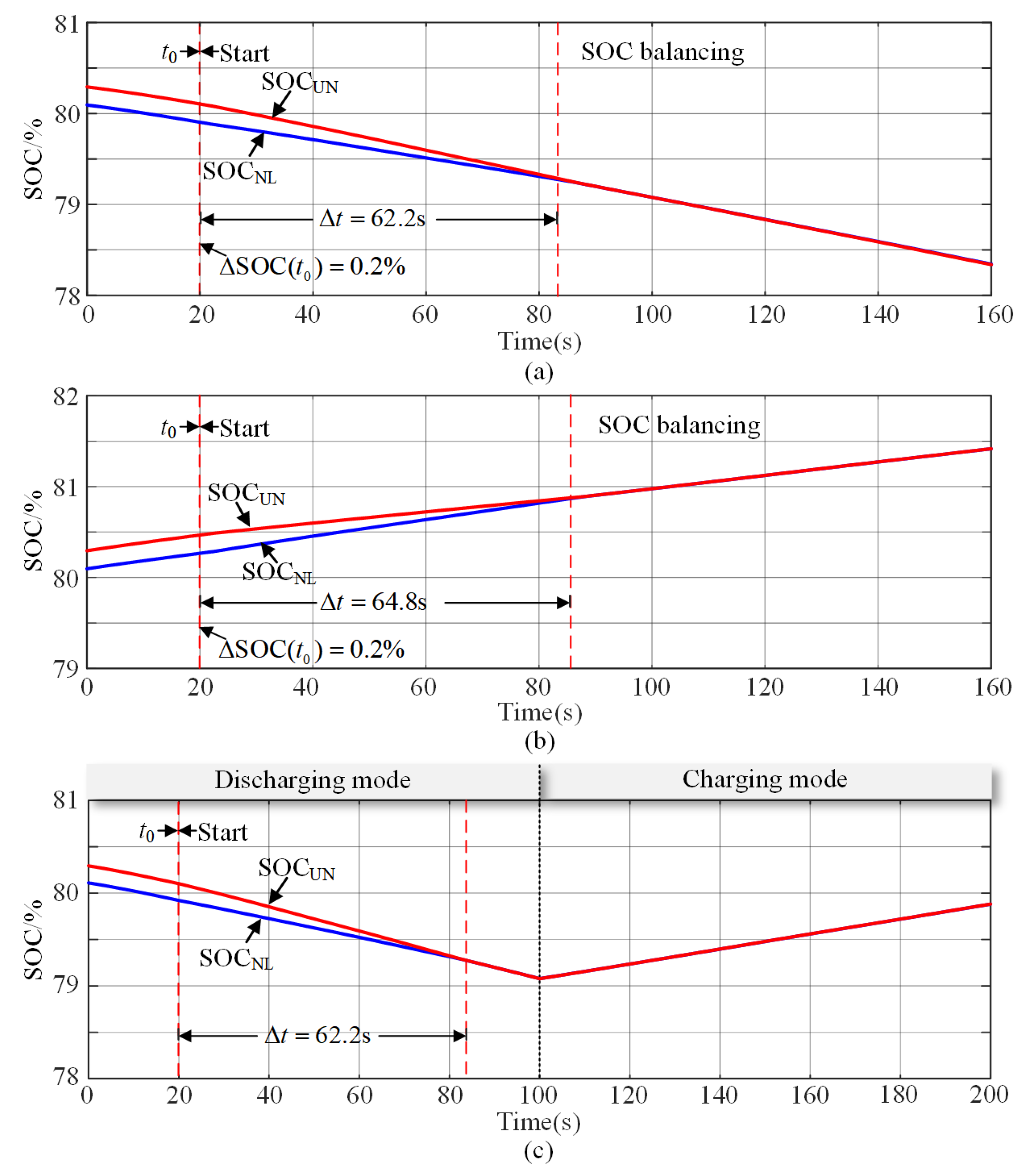
Case 1 (β = π/18): As illustrated in Figure 12, the initial ΔSOC is set at 0.2%, with the SOC balance control strategy being initiated at time t0. The simulation demonstrates that under discharging mode, SOC equilibrium between arms is achieved within Δt = 62.2 s (Figure 12a), while the charging mode requires Δt = 64.8 s to reach balance (Figure 12b). According to the system parameters provided in Table 2, the theoretical balancing time derived from Equation (24) is calculated as Δt = 60 s. The relative error between simulated and theoretical values remains below 8%, confirming the validity of the theoretical analysis. Figure 12c illustrates a transition from discharge to charge: initially, the battery is in discharge mode, and after 62.2 s, the SOC of arms reaches a balanced state; subsequently, at t = 100 s, the system switches from discharge to charge mode. The results show that despite the change in operating mode, the SOC among arms maintains good balance.
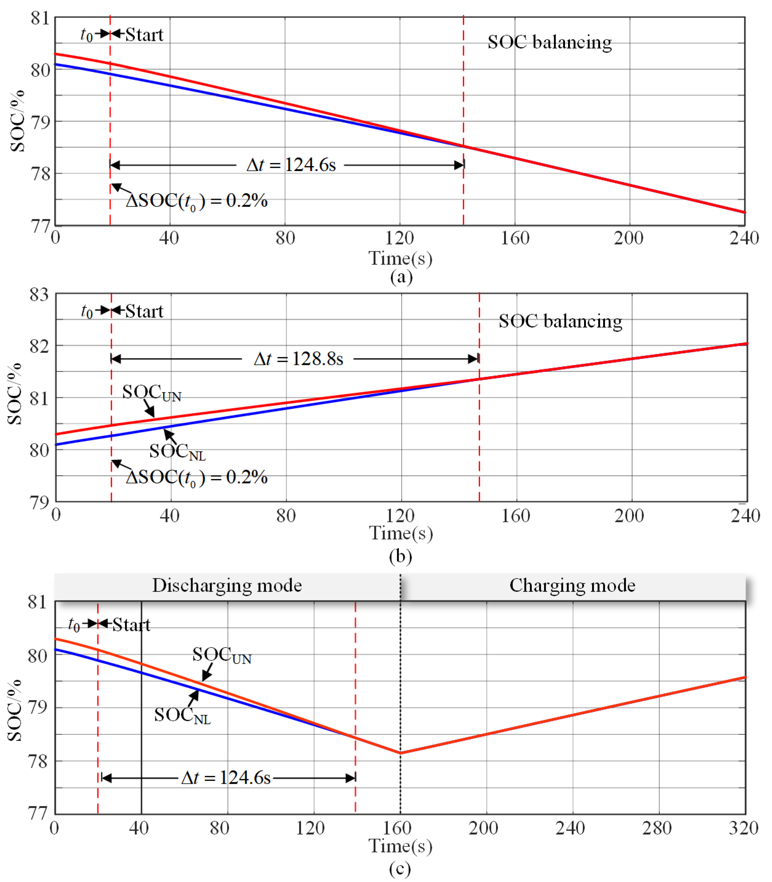
Case 2 (β = π/25): As illustrated in Figure 13, the balancing control is initiated at time t0 while maintaining an identical initial SOC difference (ΔSOC = 0.2%). Simulation results demonstrate that the balancing duration extends to Δt = 124.6 s in discharging mode and Δt = 128.8 s in charging mode. The corresponding theoretical value is calculated as 120 s based on Equation (24), with the relative error between simulation and theoretical results remaining minimal. Similarly, Figure 13c also indicates that the SOC among arms remains balanced during transition between discharge and charge mode.
The comparison of two cases reveals that when the β value is reduced, the SOC balancing time increases. This observation aligns closely with the inverse relationship indicated in Equation (24). The results not only validate the effectiveness of the proposed theoretical model but also provide significant reference for the rational selection of β values in practical applications.
It is particularly noteworthy that the proposed inter-arm SOC balance control strategy features a self-adaptive regulation capability. As illustrated in the control flow of Figure 8, the system dynamically adjusts the arm valley voltage width β in response to real-time deviations in SOC. This characteristic provides significant operational advantages: during stable operation, closed-loop feedback control effectively maintains the ΔSOC within narrow fluctuations around predefined thresholds. With reduced balancing requirements, the corresponding β value decreases proportionally, thereby minimizing degradation in output power quality. Such an adaptive mechanism optimally balances SOC performance and power quality maintenance dynamically.
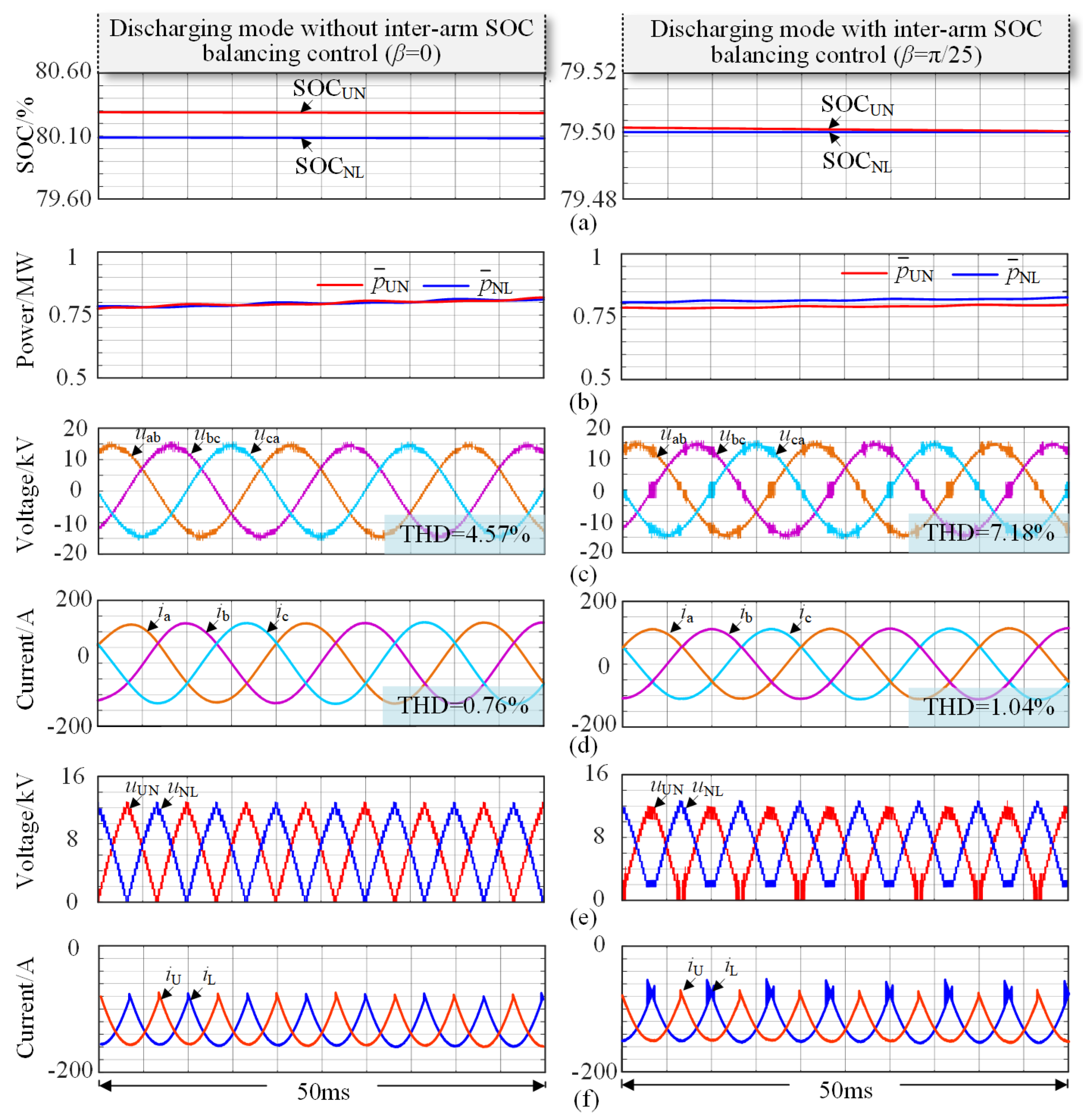
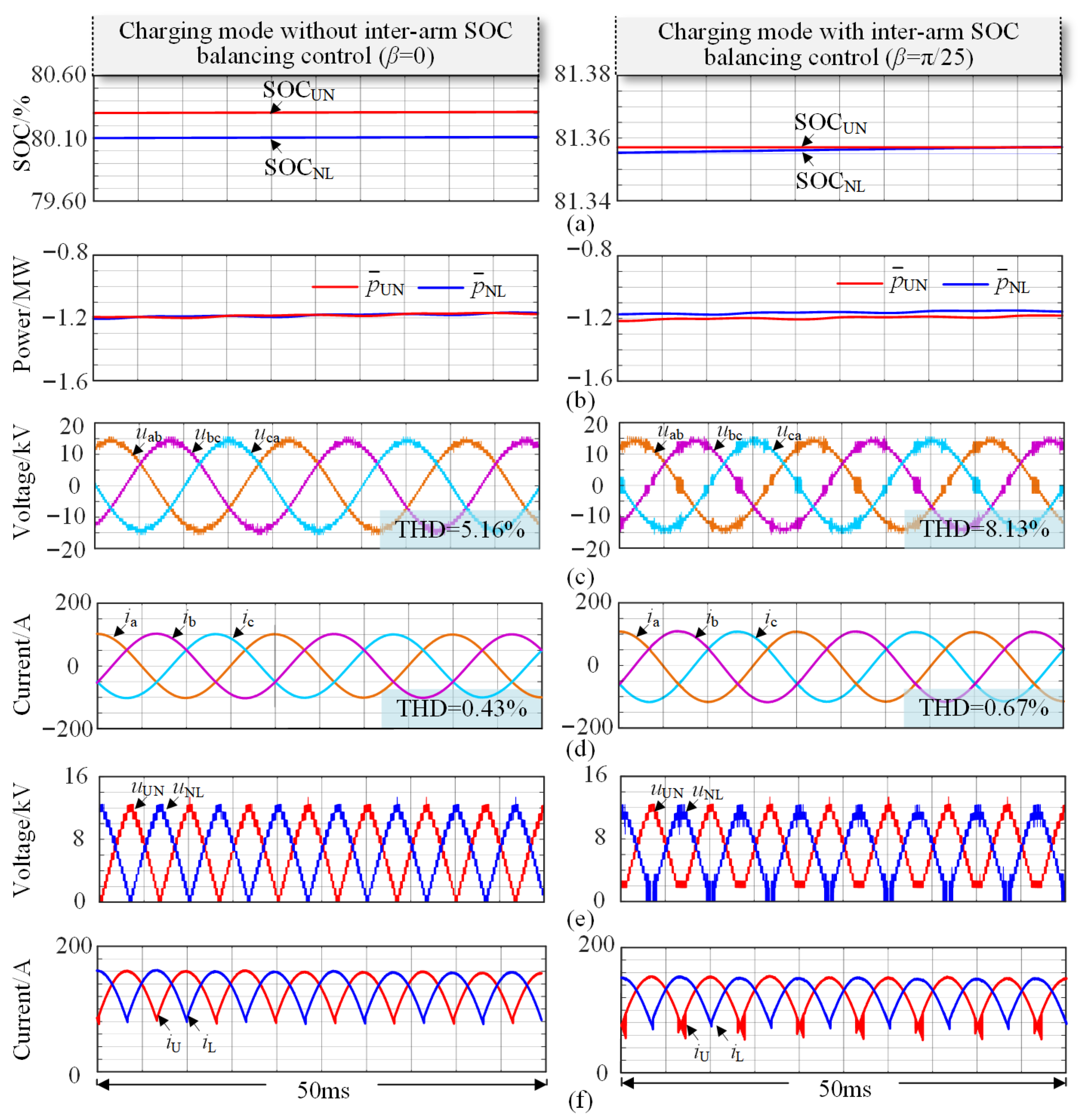
During both discharging and charging modes, the absence of a SOC balance strategy results in a significant inter-arm SOC divergence, with no tendency for convergence. This indicates an SOC imbalance despite the maintenance of power equilibrium across the arms. However, upon implementing the inter-arm SOC balance strategy, this disparity in SOC progressively diminishes; concurrently, deviations in arm power emerge, thereby confirming the efficacy of the proposed strategy. Under discharging conditions (see Figure 14c–f), the balancing strategy modifies the output characteristics of MMDTC-BESS: specifically, the THD of output voltage increases from 4.57% to 7.18%, while there is also an increase in output current THD from 0.76% to 1.04%. Similarly, during charging operations (refer to Figure 15c–f), the balancing strategy affects MMDTC-BESS’s output performance: here too, we observe an escalation in output voltage THD from 5.16% to 8.13%, alongside a rise in output current THD from 0.43% to 0.67%. Figure 14 and Figure 15 illustrate that while maintaining excellent balancing performance throughout both charging and discharging mode, this proposed strategy simultaneously impacts power quality metrics. Therefore, it is imperative that any practical implementations verify that waveform distortion rates remain within acceptable thresholds prior to applying SOC balance control.

4.2. Experimental Verification

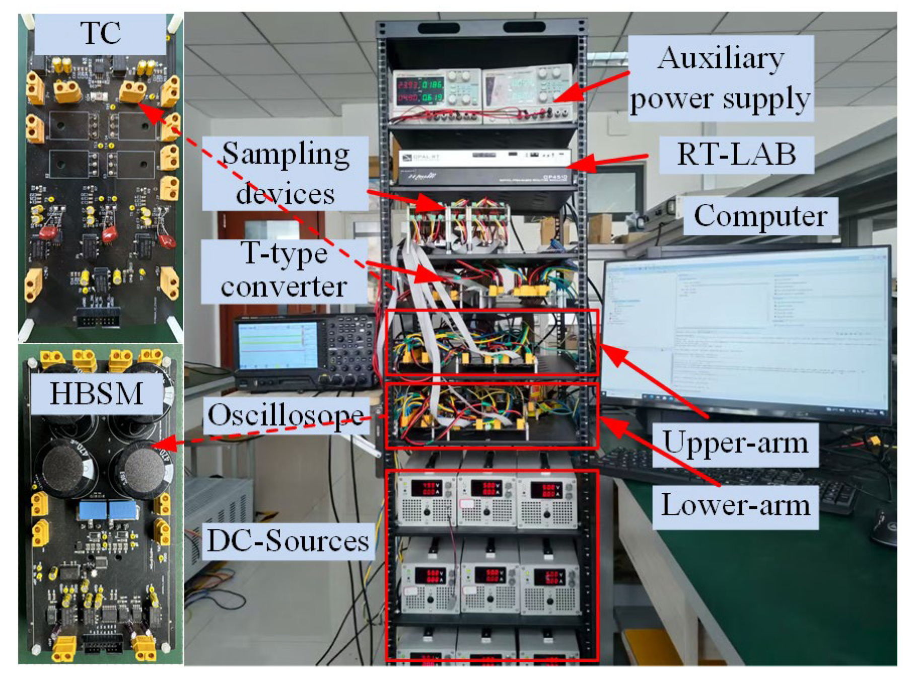
To assess the effectiveness of the proposed control strategy, an MMDTC experimental platform has been constructed, as illustrated in Figure 16, with detailed experimental parameters provided in Table 3. The main circuit is established using self-designed half-bridge submodules, while the control system is implemented on the RT-LAB real-time simulator. It is important to note that current laboratory conditions, adhering to safety regulations, do not permit the storage and maintenance of large-scale energy storage batteries in our laboratory. As a result, multiple programmable DC power supplies are utilized to replace the energy storage units, as depicted in Figure 16. This simplification does not compromise the validity of the experiment; prior theoretical analysis confirms that the core mechanism for inter-arm SOC balancing involves regulating average power distribution between the upper and lower arms.
To verify the bidirectional power regulation capability of the proposed control strategy between arms, two complementary experimental schemes were designed:
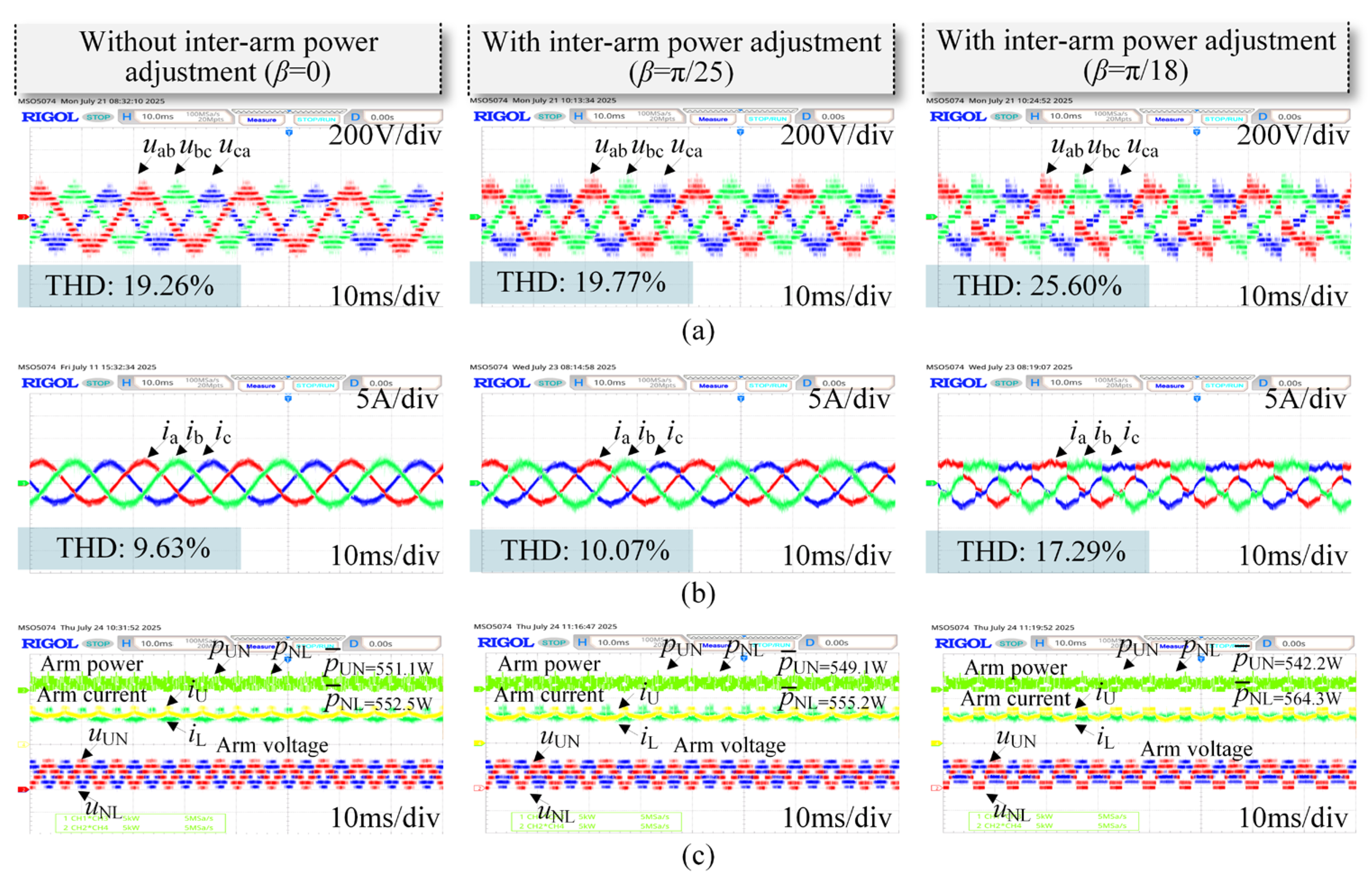
  • Case 1: Assuming a discharging condition with low SOC in the upper arm.
Solutions 3 and 4 are implemented on the upper arm and lower arm, respectively (see Figure 6), thereby replicating a typical discharging scenario where the SOC in the upper arm is lower than that in the lower arm (refer to Table 1). The experimental data is presented in Figure 17.
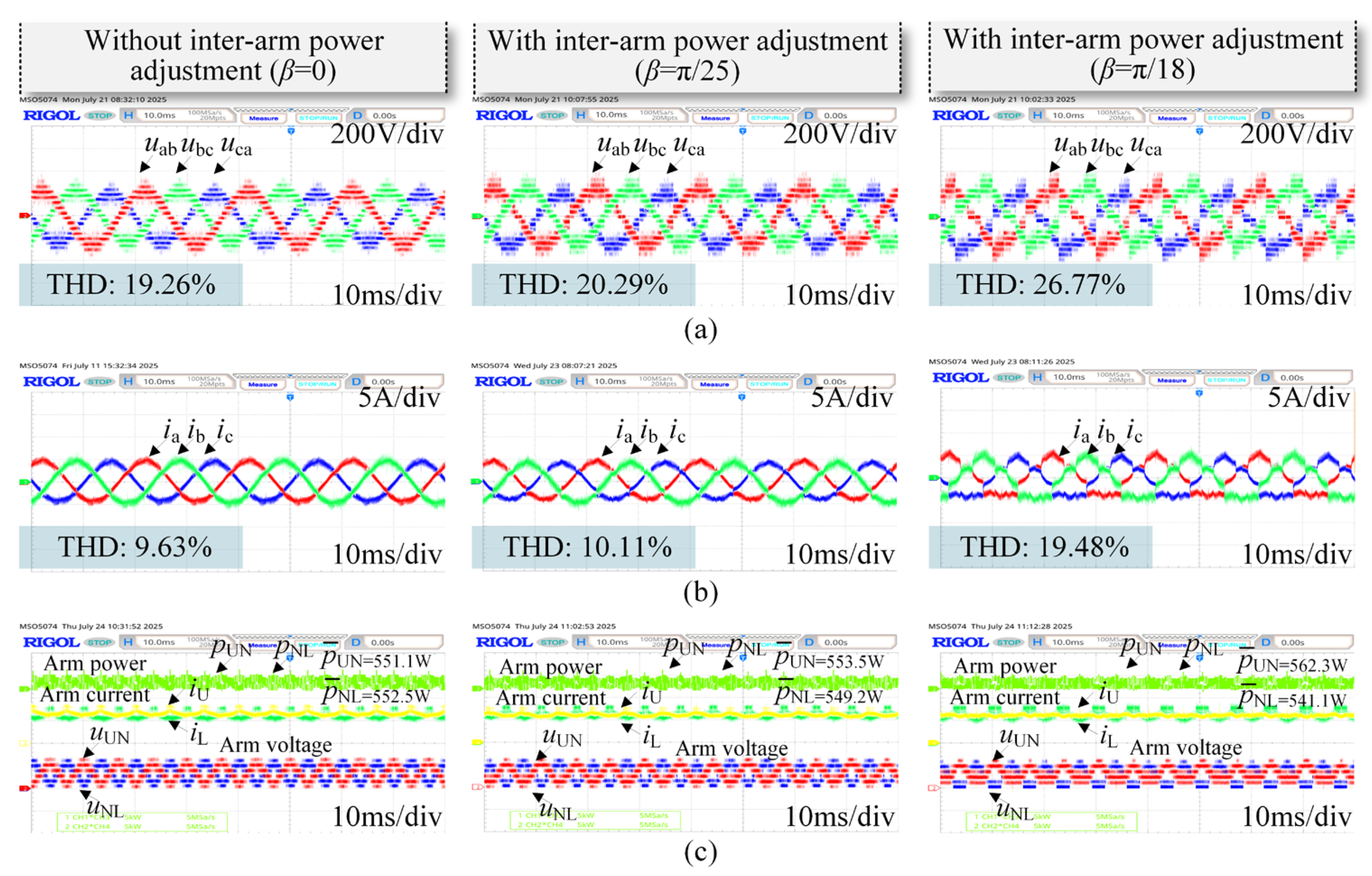
  • Case 2: Assuming a discharging condition with high SOC in the upper arm.
In this configuration, Solutions 4 and 3 are reversed, placing Solution 4 on the upper arm and Solution 3 on the lower arm. This creates a comparative scenario wherein the SOC in the upper arm exceeds that in the lower arm during discharging. The results are documented in Figure 18.
Subfigures (a)–(c) within both Figure 17 and Figure 18 illustrate output line voltage, current waveforms, as well as characteristics related to voltage/current/power for each respective arm. Key findings from these experiments include:
(1) Power quality influence
The THD of the output line voltage and current, as illustrated in subplots (a)–(b) of Figure 17 and Figure 18, is observed to increase monotonically as β rises from 0 to π/18. This observation confirms the inverse relationship between β and power quality, aligning with both theoretical predictions and simulation results.
(2) Power differential adjustment capability
Case 1 (Figure 17c) exhibits a distinct linear control characteristic, with the average power difference across the upper and lower arms measuring −1.4 W, −6.1 W, and −22.1 W at β values of 0, π/25, and π/18, respectively. Conversely, Case 2 (Figure 18c) demonstrates reversed polarity while maintaining an identical trend; it shows power differences of −1.4 W, +4.3 W, and +21.2 W, corresponding to the respective β values.
The experimental results from both schemes clearly illustrate that precise bidirectional regulation of power between the arms can be achieved by adjusting the arm valley voltage width β; furthermore, this regulation intensity exhibits a positive correlation with increasing β values.

5. Conclusions

The control strategy for inter-arm SOC balancing based on the arm valley voltage adjustment proposed in this paper successfully addresses the issue of imbalance between arms in MMDTC-BESS. By adjusting the arm valley voltage width, it disrupts the inherent power balance between the upper and lower arms. A comprehensive mathematical model has been established through theoretical analysis, deriving a quantitative relationship where the inter-arm power difference is directly proportional to the arm valley voltage width β, while SOC balancing time is inversely proportional to β. Simulation and experimental results validate both the effectiveness and practicality of this strategy; specifically, at β = π/18, approximately 4% power regulation capability can be achieved, with a high degree of correlation between theoretical predictions and measured outcomes. It is particularly noteworthy that this proposed strategy exhibits adaptive control characteristics: during steady-state operation, closed-loop feedback maintains β within a narrow range, thereby ensuring dynamic SOC equilibrium while minimizing adverse impacts on power quality. This research fills a technical gap in inter-arm SOC balancing control and lays a theoretical foundation for engineering applications of this novel topology in battery energy storage fields.

Author Contributions

Conceptualization, Q.Y.; Methodology, Q.Y. and D.N.; Software, Q.Y., D.N. and X.C.; Validation, Q.Y., X.C. and D.W.; Formal analysis, D.W.; Investigation, D.Y.; Resources, L.Z.; Data curation, D.Y. and L.Z.; Writing—original draft, X.C. and D.W.; Writing—review & editing, Q.Y. and D.N. All authors have read and agreed to the published version of the manuscript.

Funding

This work is supported by the National Natural Science Foundation of China (52407113); Natural Science Foundation of Shandong Province (ZR2024ME075), and Enterprise Project: Research and Development of Multilevel Converter for Integrated New Energy Power Generation and Energy Storage (kj20250221).

Data Availability Statement

The original contributions presented in this study are included in the article. Further inquiries can be directed to the corresponding author.

Conflicts of Interest

The authors declare no conflict of interest.

References

  1. Li, J.; Fang, Z.; Wang, Q.; Zhang, M.; Li, Y.; Zhang, W. Optimal operation with dynamic partitioning strategy for centralized shared energy storage station with integration of large-scale renewable energy. J. Mod. Power Syst. Clean Energy 2024, 12, 359–370. [Google Scholar] [CrossRef]
  2. Byrne, R.H.; Nguyen, T.A.; Copp, D.A.; Chalamala, B.R.; Gyuk, I. Energy management and optimization methods for grid energy storage systems. IEEE Access 2018, 6, 13231–13260. [Google Scholar] [CrossRef]
  3. Mei, J. Control strategies for DC microgrid energy storage systems under SOC balancing objectives. In Proceedings of the 2022 9th International Forum on Electrical Engineering and Automation (IFEEA), Zhuhai, China; 2022; pp. 386–392. [Google Scholar]
  4. Nunna, H.S.V.S.K.; Sesetti, A.; Rathore, A.K.; Doolla, S. Multiagent-based energy trading platform for energy storage systems in distribution systems with interconnected microgrids. IEEE Trans. Ind. Appl. 2020, 56, 3207–3217. [Google Scholar] [CrossRef]
  5. Cui, Y.; Dai, Q.; Du, Y.; Zhu, T.; Zhang, S. Research on new energy storage grid-connected operation system for multi-scenarios. In Proceedings of the 2024 IEEE PES 16th Asia-Pacific Power and Energy Engineering Conference (APPEEC), Nanjing, China, 25–27 October 2024; pp. 1–5. [Google Scholar]
  6. Lin, X.; Zamora, R.; Baguley, C.A. A fullyfilter-based decentralized control with state of charge balancing strategy for battery energy storage systems in autonomous DC microgrid applications. IEEE Access 2021, 9, 15028–15040. [Google Scholar] [CrossRef]
  7. Xu, X.; Bishop, M.; Oikarinen, D.G.; Hao, C. Application and modeling of battery energy storage in power systems. CSEE J. Power Energy Syst. 2016, 2, 82–90. [Google Scholar] [CrossRef]
  8. Sun, Y.; Zhong, J.; Li, Z.; Tian, W.; Shahidehpour, M. Stochastic scheduling of battery-based energy storage transportation system with the penetration of wind power. IEEE Trans. Sustain. Energy 2017, 8, 135–144. [Google Scholar] [CrossRef]
  9. Yao, L.; Yang, B.; Cui, H.; Zhuang, J.; Ye, J.; Xue, J. Challenges and progresses of energy storage technology and its application. J. Mod. Power Syst. Clean Energy 2016, 4, 519–528. [Google Scholar] [CrossRef]
  10. Elrais, M.T.; Batarseh, I. Theoretical, simulation, and experimental comparison of GaN-based two-level and multilevel converters. In Proceedings of the 2022 IEEE 7th Southern Power Electronics Conference (SPEC), Denarau Island, Fiji, 5–8 December 2022; pp. 1–6. [Google Scholar]
  11. Harbi, I.; Rodriguez, J.; Poorfakhraei, A.; Vahedi, H.; Guse, M.; Trabelsi, M.; Abdelrahem, M.; Ahmed, M.; Fahad, M.; Lin, C.-H.; et al. Common DC-link multilevel converters: Topologies, control and industrial applications. IEEE Open J. Power Electron. 2023, 4, 512–538. [Google Scholar] [CrossRef]
  12. Katayama, M.; Ohno, T.; Obara, H.; Kawamura, A. Application of multi-level converter for fast current control in small-scale DC power network. IEEE Trans. Ind. Appl. 2019, 55, 2902–2909. [Google Scholar] [CrossRef]
  13. Ding, L.; Lian, Y.; Li, Y.W. Multilevel current source converters for high power medium voltage applications. CES Trans. Electr. Mach. Syst. 2017, 1, 306–314. [Google Scholar] [CrossRef]
  14. Bernet, D.; Hiller, M. A cascaded H-bridge-based multilevel converter with low energy pulsation for high-power grid applications. IEEE Trans. Power Electron. 2024, 39, 2305–2321. [Google Scholar] [CrossRef]
  15. Niu, D.; Gao, F.; Xu, T.; Ma, Z. Thyristor-based T-type converter with modular multilevel DC-link. IEEE Trans. Power Electron. 2022, 37, 6792–6806. [Google Scholar] [CrossRef]
  16. Niu, D.; Gao, F.; Xu, T.; Ma, Z. Low-Capacitance operation and its hierarchical control for STATCOM based on T-type converter with MMDTC. IEEE Trans. Power Electron. 2025, 40, 1153–1167. [Google Scholar]
  17. Lim, W.C.; Teo, B.C.T.; Lim, X.Y.; Siek, L.; Tan, E.L. Comparative analysis of passive, active, and hybrid cell balancing for optimal battery performance. In Proceedings of the 2024 International Conference on Electronics, Information, and Communication (ICEIC), Taipei, Taiwan, 9–11 July 2024; pp. 1–4. [Google Scholar]
  18. Buchinskiy, N.; Saitoh, H. SOC balancing mechanism to improve active power sharing among multiple ESS units in low-inertia power systems. In Proceedings of the 2023 IEEE PES Innovative Smart Grid Technologies—Asia (ISGT Asia), Auckland, New Zealand; 2023; pp. 1–5. [Google Scholar]
  19. Xiaofeng, Y.; Yao, X.; Bowei, C. Enhanced modular multilevel converter based battery energy storage system. In Proceedings of the IEEE Energy Conversion Congress and Exposition (ECCE), Cincinnati, OH, USA, 1–5 October 2017; pp. 4914–4919. [Google Scholar]
  20. Wang, X.; Zhang, Y.; Dong, P.; Jia, N.; Zhu, X. Power allocation strategy for battery energy storage power station considering SOC equalization. In Proceedings of the 2023 26th International Conference on Electrical Machines and Systems (ICEMS), Zhuhai, China, 5–8 November 2023; pp. 4105–4109. [Google Scholar]
  21. Barresi, M.; De Simone, D.; Piegari, L. Direct State-of-Charge balancing control for modular multilevel converter integrating batteries. IEEE J. Emerg. Sel. Topics Power Electron. 2025, 13, 733–746. [Google Scholar] [CrossRef]
  22. Xu, J.; Wang, J.; Wang, F.; Wang, J.; Li, G. SOC balancing control based on predictive power model amongst supercapacitor packs in MMC with embedded energy storage system. IEEE Trans. Power Deliv. 2023, 38, 2641–2649. [Google Scholar] [CrossRef]
  23. Liang, G.; Rodriguez, E.; Farivar, G.G.; Yadav, G.N.B.; Beniwal, N.; Pou, J.; Konstantinou, G. A comparison of PI-based and sorting-based state of charge balancing methods in cascaded H-bridge converters. In Proceedings of the 2022 IEEE Energy Conversion Congress and Exposition (ECCE), Detroit, MI, USA, 9–13 October 2022; pp. 1–7. [Google Scholar]
  24. Bian, K.; Wu, X.; Li, H.; Huang, C.; Cai, X. A power decoupling control strategy for CHB-BESS based on NLM. In Proceedings of the 2024 9th Asia Conference on Power and Electrical Engineering (ACPEE), Shanghai, China, 11–13 April 2024; pp. 2664–2668. [Google Scholar]
  25. Lee, T.L.; Chen, Y.H.; Zheng, W.T.; Lin, C.H. Power control of repurposing-battery modular multilevel converter. In Proceedings of the 2022 IEEE Energy Conversion Congress and Exposition (ECCE), Detroit, MI, USA, 9–13 October 2022; pp. 1–7. [Google Scholar]
  26. Wang, Q. State of charge equalization control strategy of modular multilevel converter with battery energy storage system. In Proceedings of the 2020 5th International Conference on Power and Renewable Energy (ICPRE), Shanghai, China, 12–14 September 2020; pp. 316–320. [Google Scholar]
  27. Yu, X.; Wang, C.; Wang, Y.; Han, C. Arm average model and operational characteristics analysis of MMC with integrated battery energy storage system. In Proceedings of the 2023 IEEE 2nd International Power Electronics and Application Symposium (PEAS), Guangzhou, China, 10–13 November 2023; pp. 1426–1431. [Google Scholar]
  28. Pirooz, A.; Firouz, Y.; Van Mierlo, J.; Berecibar, M. Voltage vector redundancy exploitation for battery balancing in three-phase CHB-based modular energy storage systems. IEEE Trans. Ind. Electron. 2022, 69, 9364–9375. [Google Scholar] [CrossRef]
  29. Bharadwaj, V.; Panda, S.; Kundu, S.; Banerjee, S. Seven level CHB multilevel inverter based STATCOM using decoupled control and DC voltage balancing. In Proceedings of the IECON 2023-49th Annual Conference of the IEEE Industrial Electronics Society, Kolkata, India, 16–19 October 2023; pp. 1–6. [Google Scholar]
  30. Gomez, P.J.; Galvan, L.; Galvan, E.; Carrasco, J.M. Energy storage systems current ripple reduction for DC-link balancing method in hybrid CHB topology. In Proceedings of the IECON 2020 The 46th Annual Conference of the IEEE Industrial Electronics Society, Singapore, 18–21 October 2020; pp. 1808–1813. [Google Scholar]
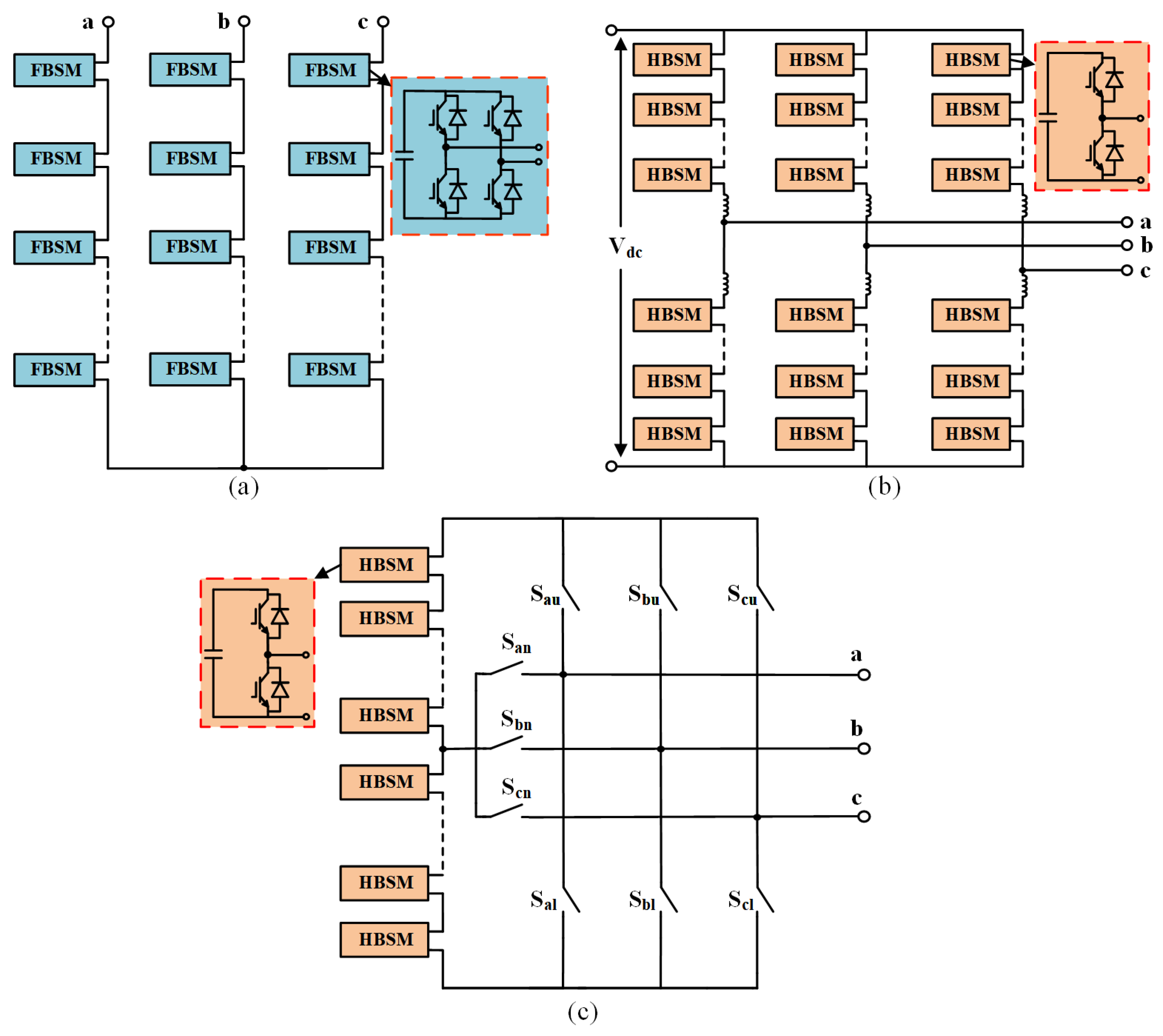
Figure 1. Multilevel topology: (a) CHB; (b) MMC; (c) MMDTC.
Applsci 15 10196 g001
Figure 2. Diagram illustrating the causes and corresponding solutions for battery SOC imbalance.
Applsci 15 10196 g002
Figure 3. Topology of MMDTC-BESS.
Applsci 15 10196 g003
Figure 4. The relationship among (a) output phase currents, (b) output phase voltages, (c) output line voltages, (d) arm currents, and (e) arm voltages.
Applsci 15 10196 g004
Figure 5. Schematic diagram of arm valley voltage adjustment of (a) initial arm valley voltage (zero voltage) (b) increase zero voltage interval (from zero to β), and (c) Increase arm valley voltage value and interval.
Applsci 15 10196 g005
Figure 6. Arm valley voltage adjustment scheme of (a) reducing the charging power (namely Solution 1), (b) increasing the charging power (namely Solution 2), (c) reducing the discharging power (namely Solution 3), and (d) increasing the discharging power (namely Solution 4).
Applsci 15 10196 g006
Figure 7. The relationship curve between β and μ .
Applsci 15 10196 g007
Figure 8. Flow chart of the proposed inter-arm SOC balancing control.
Applsci 15 10196 g008
Figure 9. Overall control block diagram of the MMDTC-BESS: (a) control of MMDTC, (b) power control and (c) individual submodule SOC balancing control.
Applsci 15 10196 g009
Figure 10. Output voltage waveform using the proposed inter-arm SOC balancing control.
Applsci 15 10196 g010
Figure 11. Relationship between arm valley voltage adjustment interval width β and harmonics: (a) curve of β versus THD and (b) curve of β versus individual harmonic components.
Applsci 15 10196 g011
Figure 12. Arm SOC curves when β = π/18 under (a) discharging mode, (b) charging mode and (c) discharge/charge state transition.
Applsci 15 10196 g012
Figure 13. Arm SOC curves when β = π/25 under (a) discharging mode, (b) charging mode and (c) discharge/charge state transition.
Applsci 15 10196 g013
Figure 14. Simulation waveforms of (a) arm SOC, (b) arm average power, (c) output line-voltages, (d) output currents, (e) arm voltages, and (f) arm currents under the discharging mode.
Applsci 15 10196 g014
Figure 15. Simulation waveforms of (a) arm SOC, (b) arm average power, (c) output line-voltages, (d) output currents, (e) arm voltages, and (f) arm currents under the charging mode.
Applsci 15 10196 g015
Figure 16. Photograph of MMDTC prototype.
Applsci 15 10196 g016
Figure 17. Experimental results of (a) output line voltages, (b) output currents, (c) arm voltages, arm currents, and arm powers under Case 1.
Applsci 15 10196 g017
Figure 18. Experimental results of (a) output line voltages, (b) output currents, (c) arm voltages, arm currents, and arm powers under Case 2.
Applsci 15 10196 g018
Table 1. Arm valley voltage adjustment scheme determined based on battery charging/discharging state and SOC difference across arms.
Charging State Discharging State
SOC UN > SOC NL SOC UN < SOC NL SOC UN < SOC NL SOC UN > SOC NL
Upper-armSolution 1Solution 2Solution 3Solution 4
Lower-armSolution 2Solution 1Solution 4Solution 3
Table 2. Main parameters list of simulation.
VariableSymbolValue
Rated grid line voltage V line 10 kV
Rated active powerP2 MW
Rated reactive powerQ0
Grid-side filtering inductanceL5 mH
Number of submodules per armN20
Battery pack voltage U b 800 V
Rated capacity of Battery C rate 200 Ah
Submodule capacitance C sm 0.47 mF
Switching frequencyfs1.5 kHz
Threshold   value   of   SOC ε 1 × 10 5
Table 3. The main experimental parameters.
VariableSymbolValue
Grid voltage V g 110 V
Rated amplitude of phase current I O 5 A
Grid-side filtering inductanceL4 mH
Number of submodules per armN5
DC voltage of submodule U b 50 V
Submodule capacitance C sm 0.2 mF
Switching frequencyfs5 kHz
Disclaimer/Publisher’s Note: The statements, opinions and data contained in all publications are solely those of the individual author(s) and contributor(s) and not of MDPI and/or the editor(s). MDPI and/or the editor(s) disclaim responsibility for any injury to people or property resulting from any ideas, methods, instructions or products referred to in the content.